Universal Fabrication of Two-Dimensional Electron Systems in Functional Oxides
This is the peer reviewed version of the following article: T. C. Rödel, F. Fortuna, S. Sengupta, E. Frantzeskakis, P. Le Fèvre, F. Bertran, B. Mercey, S. Matzen, G. Agnus, T. Maroutian, P. Lecoeur, and A. F. Santander-Syro. Universal fabrication of 2D electron systems in functional oxides. Adv. Mater. 28, 1976-1980 (2016), which has been published in final form at https://doi.org/10.1002/adma.201505021. This article may be used for non-commercial purposes in accordance with Wiley Terms and Conditions for Use of Self-Archived Versions.
Table of contents entry
Two-dimensional electron systems (2DESs) in functional oxides are promising for applications, but their fabrication and use, essentially limited to SrTiO3-based heterostructures, are hampered by the need of growing complex oxide over-layers thicker than 2 nm using evolved techniques. This work shows that thermal deposition of a monolayer of an elementary reducing agent suffices to create 2DESs in numerous oxides.
Keyword: 2DES in oxide surfaces and interfaces.
![[Uncaptioned image]](/html/2102.07748/assets/x1.png)
A critical challenge of modern materials science is to tailor novel states of matter suitable for future applications beyond semiconductor technology. Two-dimensional electron systems (2DESs) in multi-functional oxides [1] can show metal-to-insulator transitions [2], superconductivity [3, 4], magnetism [5, 6, 7], or spin-polarized states [8, 9, 10], and are thus an active field of current research [11, 12, 13]. However, the fabrication of 2DESs in oxide heterostructures, like LaAlO3/SrTiO3, requires growing a layer of binary (e.g. Al2O3) or ternary (e.g. LaAlO3) oxides with a “critical thickness” of at least 20 Å using evolved deposition techniques, such as pulsed laser deposition [1, 14, 11, 12, 13, 15, 16, 17]. Thus, the reproducibility of their properties depends crucially on the growth parameters, while their fabrication is complex, expensive, and unsuitable for mass production. Moreover, the existence of a critical thickness of 20 Å for the onset of conductivity severely limits the control of the 2DES’s properties, hampering tunneling spectroscopy studies or applications that rely on charge or spin injection [18]. Similarly, the realization of 2DESs at the surface of SrTiO3 or other oxides requires the use of intense UV or X-ray synchrotron radiation, to desorb oxygen from the surface [19, 20, 21, 22, 23, 24, 25, 26]. Thus, these 2DESs can be only manipulated and studied in ultra-high vacuum (UHV), to preserve the vacancies from re-oxidation, and are obviously not suited for experiments or applications at ambient conditions.
Here we demonstrate a new, wholly general, extremely simple and cost-effective method to generate 2DESs in functional oxides. We use thermal evaporation from a Knudsen cell to deposit, at room temperature in UHV, an atomically-thin layer of an elementary reducing agent, such as pure aluminum, on the oxide surface. Due to an efficient redox reaction, the Al film pumps oxygen from the substrate, oxidizes into insulating AlOx, and forms a pristine, homogeneous 2DES in the first atomic planes of the underlying oxide. The principle of redox reactions induced by metals at the surface of oxides is well documented [28, 27]. However, the simple idea of using a pure, elementary reducing agent to create a 2DES at a metal-oxide interface was not explored so far. This overcomes the complexity of growing an oxide thin film, the requirement of a critical thickness of insulating capping layer to create the 2DES in UHV, and the necessity, in the case of surfaces, of strong synchrotron radiation to desorb oxygen. As a novel application, we extend this method to generate a 2D metallic state at the surface of the room-temperature ferroelectric BaTiO3. Such hitherto unobserved coexistence of ferroelectricity and 2D conductivity in the same material is promising for functional devices using ferroelectric resistive switching [29, 30]. This new, simpler and cheaper, fabrication route for 2DESs is thus adaptable to numerous oxides, given that oxygen vacancies are shallow donors in these materials, resulting in itinerant electrons. Moreover, this technique is scalable to industrial production, and ideally suited for applications that rely on charge or spin injection and for the realization of mesoscopic devices.
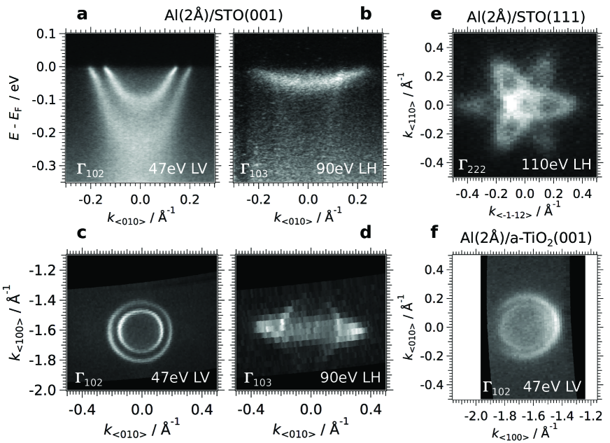
The existence of a 2DES at the interface between the oxidized Al layer and SrTiO3(001), SrTiO3(111) and anatase-TiO2(001) is evidenced by our angle-resolved photoemission spectroscopy (ARPES) data presented in Figure 1 –see the Supporting Information for details about the surface preparation, Al deposition, and ARPES measurements. For simplicity, and to recall that we are simply depositing pure Al (not aluminum oxide) on top of the oxide surfaces, all throughout this paper we note the resulting oxidized Al capping layer simply as “Al”, specifying in parenthesis the evaporated thickness. The energy-momentum and Fermi surface maps formed by the orbitals, shown in Figure 1, agree with previous ARPES studies at the reduced surface of these materials [19, 20, 31, 24, 25, 26], demonstrating that in both cases the same 2DESs are observed.
Note that, instead of the local creation of oxygen vacancies using an intense UV beam, the evaporated Al reduces the whole surface homogeneously. As a consequence, the data quality, evidenced by the line widths, is also much better than in previous studies. Thus, as shown in Figure 1(a), a kink and change in intensity in the dispersion of the light bands at meV, attributed to electron-phonon coupling [32], can be very clearly distinguished.
The Fermi-surface areas and, hence, the charge carrier densities of the 2DESs at the Al/SrTiO3(111) and Al/TiO2(001) interfaces are about and times larger than their counterparts at the surfaces reduced by photons, probably due to a higher and more homogeneous concentration of oxygen vacancies.
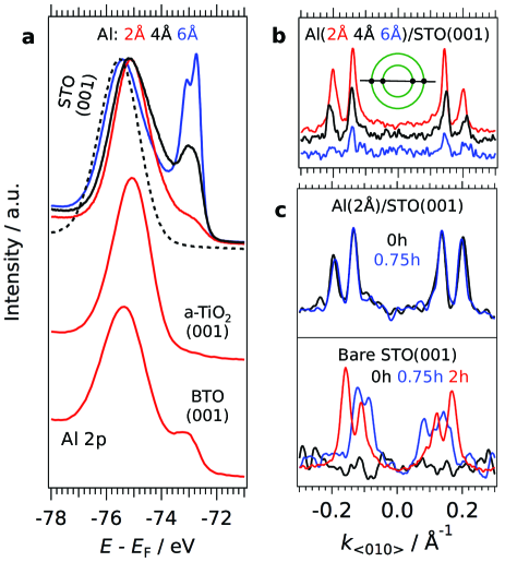
To understand the redox reaction at the Al/oxide interface, we probed the oxidation state of Al by measuring the Al- core levels, whose binding energies are very different for metallic and oxidized Al. As shown in Figure 2(a), the two contributions can be distinguished in the Al(6Å)/STO spectrum (blue curve), with the metallic component around eV binding energy and the oxidized part around eV binding energy. In contrast, the metallic Al component decreases for a thinner 4Å film (black curve), and the deposition of only 2Å of pure Al results in a nearly fully oxidized film of Al (red curves). In other words, an ultra-thin layer of 2Å of pure Al is sufficient to pump the oxygen from the surface region of all the oxides studied in this work. The spatial distribution of the oxygen vacancies close to the interface is discussed in the Supporting Information. Note that the oxidation of the metallic Al results in an increased layer thickness: as the mass density of Al is g/cm3 and the one of amorphous Al2O3 is about g/cm3, the deposition of 2Å of Al yields an oxidized Al film of 2.5Å.
To determine if the thickness of the Al-layer has an influence on the electron density of the 2DES, we turn to the momentum distribution curves (MDCs) at the Fermi level as shown in Figure 2(b). As can be seen in Figure 2(b), the Fermi momenta are essentially the same, within Å-1 for the 2Å (red MDC), 4Å (black) and 6Å (blue) thick Al films. As the 2D density of electrons depends solely on the Fermi momenta, it is clear that this electron density already saturates at an Al film thickness of 2Å. Thus, our method overcomes the necessity of a “critical thickness” of capping layer to generate a 2DES in UHV.
Previous studies on the bare surface of SrTiO3 prepared in-situ showed that synchrotron UV-irradiation was necessary to create the oxygen vacancies responsible for the 2DES [20, 31, 25, 26]. This is again demonstrated in the lower panel of Figure 2(c), which shows the evolution with time of the MDC at upon UV-irradiation on a bare SrTiO3(001) surface. While the 2DES is absent at h (black MDC), its carrier density increases up to saturation upon UV irradiation (blue and red MDCs), as denoted by the increase of for increasing exposure times.
Contrary to the bare surface, there is no measurable influence of the UV irradiation on the electronic structure of the Al/SrTiO3 system, neither on the charge carrier density nor on the line-shapes or spectral weight of the 2DES, as demonstrated in the top panel of Figure 2(c): the MDCs at show a stable subband structure and a maximum electron density from the very beginning of the measurements. This indicates that the oxygen vacancy concentration and distribution, due the redox reaction at the interface between Al and SrTiO3, is already saturated and stable upon irradiation.
As demonstrated in the Supporting Information, the 2DES at the interface of oxidized Al/SrTiO3 is stable also at room temperature, while the deposition of an Al film of 10Å or more on SrTiO3 minimizes the re-oxidation of vacancies in air.
We now show that the deposition of an ultra-thin Al film can also be used to create a 2DES at the surface of the room-temperature ferroelectric BaTiO3 (BTO), thus constituting a new type of confined metallic state on a truly room-temperature functional oxide. Our BTO samples are (001)-oriented thin films (thickness nm) epitaxially grown on SrTiO3(001) –see Supporting Information for details about thin-film growth, piezo-response force microscopy (PFM), and capacitance-voltage (C-V) measurements. In contrast to the bulk crystals, which usually exhibit ferroelectric-domain stripes of period nm, even down to nm scale thicknesses [33], the nm-thick BTO films deposited on Nb:STO show a single domain state, with the ferroelectric polarization aligned along the axis, due to the in-plane compressive strain induced by the epitaxial growth [34, 35, 36].
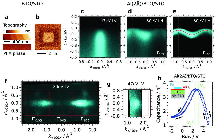
The absence of ferroelectric domains and the local reversibility of the polarization are demonstrated in Figures 3(a, b) by the simultaneous atomic force microscopy (AFM) and PFM images of a BaTiONb:SrTiO3 thin film.
The energy-momentum ARPES intensity maps of Figures 3(c-e) prove the formation of metallic itinerant states at the surface of the BTO(001) thin-film after deposition of 2 Å of Al. The resulting 2DES is constituted of a light (-like) and a heavy (-like) electron pocket around , best observed in Figures 3(c, d) with LV and LH polarizations, respectively. Such light-polarization-dependent selection rules are typical for -like states observed at the surface of other titanates, such as SrTiO3 and anatase [19, 26]. In the case of BaTiO3, the light band forms a strong peak of spectral weight whose intensity is cut-off at –see Figure 3(c). Although we cannot observe a dispersive feature within this peak of intensity, its binding energy indicates that the conduction band bottom is filled up with itinerant electrons. The heavy band, on the other hand, presents a clear dispersion –see Figures 3(d, e). A tight-binding fit of this band, red curve in Figure 3(e), yields a band bottom of meV at , a band top of meV at the zone edge, and an effective mass near of approximately .
Figures 3(f, g) show that the spectral weight at is composed of a central disc formed by the light electron pocket, best seen in Figure 3(g), and two orthogonal Fermi-surface strips spanning the entire Brillouin zone, formed by the heavy bands. These last correspond to the elliptical Fermi sheets observed at the surface of SrTiO3(001), as in Figure 1(d), but in the case of BaTiO3(001) they extend beyond the zone boundary, thus forming open Fermi sheets. From Figure 3(g), the distribution of spectral weight at for the circular Fermi surface spans a Fermi momentum Å-1. The Fermi strips can be approximated as rectangles of long and short sides (with Å the size of the square unit cell at the BTO surface) and Å-1. From the total area enclosed by all the Fermi surfaces, the density of carriers of the 2DES at the BaTiO3(001) surface is cm-2, which is comparable to the density of states at the SrTiO3 or anatase-TiO2 surfaces. The Supporting Information presents additional data showing the Fermi momenta extracted from fits to the spectra, and the photon-energy dependence of the electronic structure.
Finally, Figure 3(h) shows a measurement of the capacitance-voltage curve on the same Al(2Å)/BaTiO3 interface that was measured by ARPES. The “butterfly” shape, with a difference of about V between the two coercive voltages, demonstrates that the BTO film is still ferroelectric after deposition of the Al layer and ARPES measurements, thus keeping its functional behavior.
A 2DES at the surface of BaTiO3 is in essence an intrinsic metal/ferroelectric interface. Polarization switching of the bulk material, for instance by strain, could allow a direct gating of the 2DES, while a sufficiently thick capping alumina layer protects it against re-oxidation at ambient conditions, and can be even used to draw metallic nano-circuits of intrinsic ferroelectric tunnel junctions. Thus, this system provides a realistic platform for the realization of non-volatile memories using ferroelectric resistive switching [29, 30] or for ultra-sensitive strain or pressure detectors.
In conclusion, the method we present here for realizing 2DESs in oxides has the advantages of simplicity and versatility –for instance, it can be readily implemented in many UHV setups, allowing future investigations of 2DESs in complex oxides using non-synchrotron based spectroscopic techniques, like tunneling or Raman spectroscopies. This method is also pertinent for the study of transport phenomena in mesoscopic oxide devices. Indeed, STO has emerged as an exciting nano-electronics device platform [37], owing to the existence of superconductivity, spin-orbit interaction and magnetism which are controllable with a gate voltage. Our work opens up new possibilities to explore these questions by making a class range of transition-metal oxide 2DESs suitable for transport, including the surfaces which are candidates for hosting topological electronic states [23, 24]. Furthermore, the stability of the 2DES in ambient conditions can be achieved through a sufficiently thick layer of oxidized Al. This opens the possibility to integrate TMO 2DESs into functional devices without the need of evolved deposition techniques.
Experimental Section
The ARPES measurements were conducted at the CASSIOPEE beamline of Synchrotron SOLEIL (France). We used linearly polarized photons in the energy range eV and a hemispherical electron analyzer with vertical slits. The angular and energy resolutions were and 15 meV. The mean diameter of the incident photon beam was smaller than 100 m. The samples were cooled down to K before measuring. Unless specified otherwise, all data were taken at that temperature. The results have been reproduced on more than 10 samples for SrTiO3(001), and on at least two samples for other surface orientations and for TiO2 anatase, and on 3 thin films of BaTiO/SrTiO3(001). All through this paper, reciprocal-space directions and planes are defined in the conventional cell of each material (cubic for SrTiO3, simple tetragonal for anatase and BaTiO3). The indices , , and of correspond to the reciprocal lattice vectors of the cubic unit cell (SrTiO3 and BaTiO3) or body-centered tetragonal unit cell (anatase).
Additional details on the sample and surface preparation, the Al deposition conditions, and the piezo-response force microscopy and capacitance-voltage measurements can be found in the Supporting Information.
Acknowledgements
We thank illuminating discussions with M. Gabay and M. J. Rozenberg, and V. Pillard for help with the sample preparation. This work is supported by public grants from the French National Research Agency (ANR), project LACUNES No ANR-13-BS04-0006-01, and the “Laboratoire d’Excellence Physique Atomes Lumière Matière” (LabEx PALM project ELECTROX) overseen by the ANR as part of the “Investissements d’Avenir” program (reference: ANR-10-LABX-0039). T. C. R. acknowledges funding from the RTRA–Triangle de la Physique (project PEGASOS). A.F.S.-S. thanks support from the Institut Universitaire de France.
Supporting Information
Sample and surface preparation and Al deposition
The non-doped, polished crystals of SrTiO3 were supplied by CrysTec GmbH, the anatase crystals by SurfaceNet GmbH. To prepare the SrTiO3 surfaces, the samples were ultrasonically agitated in deionized water, subsequently etched in buffered HF and annealed at 950∘C for three hours in oxygen flow. This results in Ti-terminated (001) or (111) surfaces with terraces of width to nm separated by steps, as verified by atomic-force microscopy (AFM) in contact mode (data not shown here).
The BTO 300Å-thick films were prepared by Laser-MBE using a sintered BTO target. A Kr-F excimer laser was used for the deposition. The substrate, which was etched prior to the deposition to obtain a TiO2 terminating layer, was glued to the heater with silver paste. The growth of the film, monitored by reflection high-energy electron diffraction (RHEED), was carried out at 650 ∘C in 5x10⁻⁴ mbar oxygen pressure with 0.1 % ozone. RHEED oscillations were used to measure the deposited thickness. At the end of the deposition, the films were cooled down in 6x10⁻³ mbar oxygen pressure, always with 0.1% ozone.
To clean the surfaces in UHV, the SrTiO3 samples were annealed at a temperature ∘C for min at pressures lower than mbar. The anatase crystals were prepared by Ar+ sputtering ( kV, min) and annealing cycles ( ∘C, min,) similar to the procedure described by Setvin et al. [38]. The surface of the BaTiO3 thin films was cleaned by annealing the samples at temperatures C for min. One of the samples was Ar+ sputtered ( V, min) prior to the UHV annealing, without noticeable changes in the ARPES data.
The surface quality and the possible existence of surface reconstructions was probed by low-energy electron diffraction (data not shown here). The SrTiO3(001) and BaTiO3(001) surfaces are unreconstructed, whereas the (111) surface shows a reconstruction, and the anatase (001) surface shows a two-domain reconstruction.
To create a local, high concentration of oxygen vacancies in the surface region of SrTiO3, TiO2 anatase, or BaTiO, amorphous Al-films with thicknesses between Å were deposited on the prepared surface of the crystals. Aluminium was evaporated from a Knudsen cell using an alumina crucible. The growth rate was approximately Å /min, corresponding to a temperature of about 925∘C of the crucible. The Al-flux was calibrated prior to the evaporation using a quartz microbalance. The cleanliness of the deposit was checked by evaporating a thin Al-film on a Cu substrate where no oxidation could be detected by Auger spectroscopy. The temperature of the crystals ranged between ∘C during the Al deposition.
Piezo-response force microscopy and capacitance-voltage measurements
For the PFM measurements, a probing signal of V at a frequency of 25 kHz was applied to a Co/Cr coated cantilever with N/m force constant. A lower probing signal of V was also used with no change on the observed phase images such as the ones shown in Figure 3(a) of the main text. In order to assess the ferroelectric character of the BTO film measured by ARPES, m-diameter Pd electrodes ( nm thickness) were deposited through a shadow mask on top of the Al oxide (AlOx) layer. The C-V measurements were performed using a LCR meter with a mV AC amplitude at kHz, while a source-meter allowed for the DC biasing with V steps of ms duration. The C-V curve, Figure 3(h) of the main text, shows the characteristic butterfly shape of a ferroelectric material. Note that due to the ultra-thin AlOx layer, the required voltages to reverse the polarization () are rather high and shifted towards the positive voltage side, indicating an internal upward electric field in the BTO layer. For these reasons it was not possible to achieve a polarization reversal in PFM configuration on this sample.
Homogeneity of the 2DES
Previous studies of the 2DES at the surface of SrTiO3 were conducted on fractured [19, 20] or in-situ prepared surfaces [31, 24]. The fracturing process results in locally ordered surfaces [39], while the in-situ preparation results in an ordered surface. The fracturing process or intense UV light irradiation at low temperature (spot size m) create a local, high concentration of oxygen vacancies in the surface region of SrTiO3 whose electrons (partly) dope the 2DES.
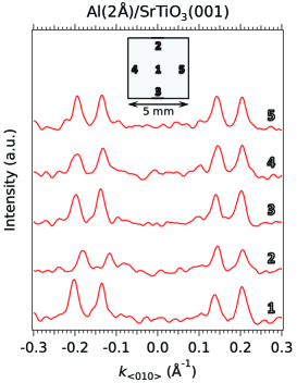
In contrast to such spatial inhomogeneity of the 2DES in fractured or UV irradiated bare SrTiO3, the fact that we cannot observe any changes induced by the synchrotron light at the Al/SrTiO3 interface (Figure 2(c) of the main text) suggests that the underlying SrTiO3 surface is reduced homogeneously. This is explicitly shown in Figure 4, which presents the momentum distribution curves at measured at five different positions on the Al(2Å)/SrTiO3 interface. We observe that the Fermi momenta, given by the MDC peaks, are independent of the measurement point, demonstrating the homogeneity of the interfacial 2DES over distances of several millimeters.
Temperature dependence of the electronic structure of the 2DES at the Al/SrTiO3(001) interface
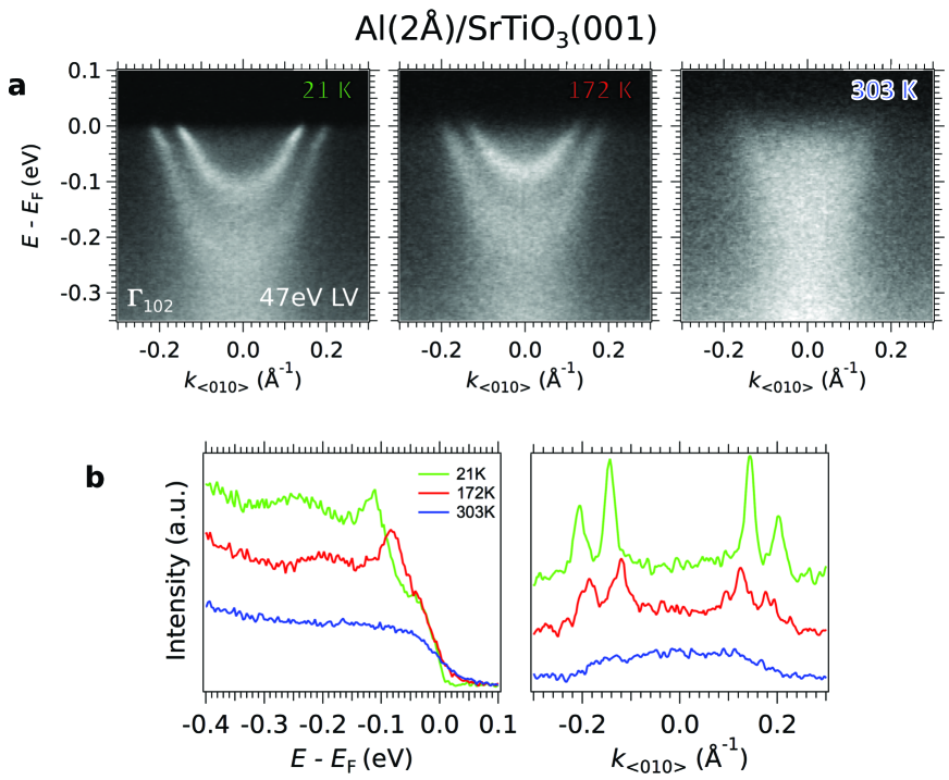
Figure 5(a) shows the energy-momentum maps at the Al/SrTiO3 interface measured respectively at 21 K, 172 K, and 303 K, under the same conditions as the map in Figure 1(a) of the main text. The dispersions of the two light bands of -character are still clearly visible at K although the line widths are increased due to thermal broadening. At K, the line widths are too large to identify the individual bands, although the left branch of the outer band is still visible close to the Fermi level . Nevertheless, the spectral weight at the Fermi level demonstrates the existence and stability of the 2DES at room temperature. To compare the energy-momentum maps more directly, Figure 5(b) shows the energy distribution curves at and the momentum distribution curves at Fermi level . As can be seen from the value of the Fermi momenta of the peaks in the MDCs as well as the binding energies of the peaks in the energy distribution curves (EDCs), the charge carrier density decreases slightly when temperature increases. We checked (not shown) that these results are reproducible upon thermal cycling.
Effect of exposure to ambient conditions
In principle, the thicker the oxidized Al film the better the passivation
of the surface against re-oxidation in ambient air pressure.
For amorphous Al2O3 films grown by atomic layer deposition on the surface of SrTiO3(001),
a film thickness of nm is sufficient to create a stable 2DES
at the Al2O3/SrTiO3 interface [16].
Note that this value is identical to the thickness of the natural oxidized layer
at the surface of aluminum ( nm) [40].
Hence, this thickness is sufficient to prevent oxygen diffusion
through a homogenous Al2O3 capping layer.
In our case, the probing depth of the high-resolution ARPES measurements,
such as the ones shown in the main text,
is limited by the mean free path of electrons which is Å at kinetic energies
of eV.
To increase the probing depth and probe the 2DES at buried interfaces,
e.g. LaAlO3/SrTiO3, soft x-ray angle-resolved resonant photoelectron spectroscopy
was applied previously [41].
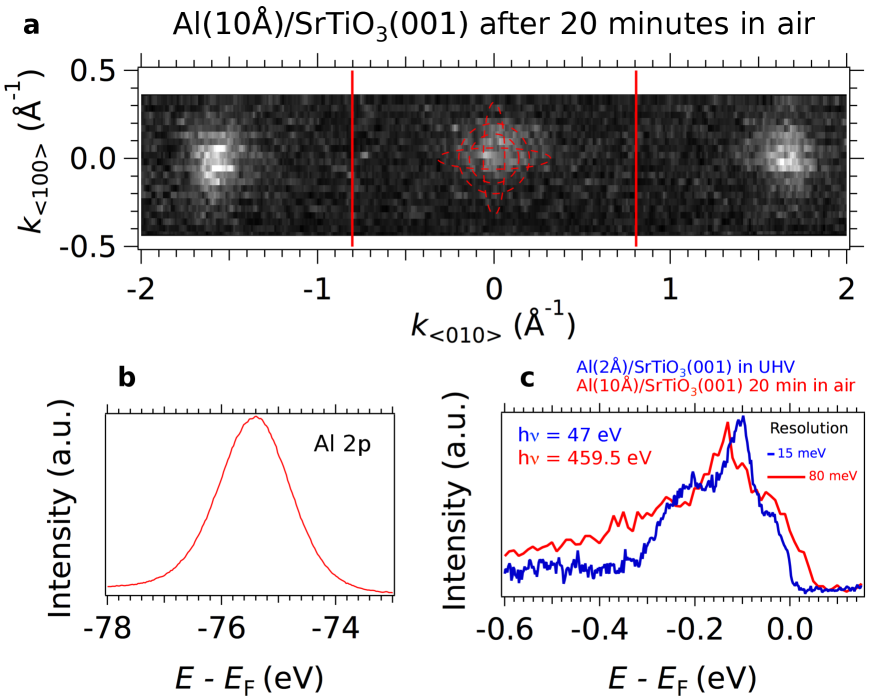
Thus, to test the stability of the 2DES, we exposed an Al(10 Å)/SrTiO3 sample
to ambient conditions for about 30 minutes,
and conducted soft x-ray resonant ARPES (=459.5 eV) at low temperatures.
Note that nm of Al corresponds to about nm of Al2O3
which is close to the “critical” passivation thickness mentioned above.
As can be seen from the Fermi surface in Figure 6(a), the 2DES at the Al(10 Å)/SrTiO3 interface still exists after the exposure to air. For comparison, the red dashed circles and ellipses represent the Fermi surfaces measured at the ultra-thin Al(2 Å)/SrTiO3 interface –see Figures 1(c, d) of the main text. Note that the 10 Å Al layer was completely oxidized after exposure to air, as demonstrated by the peak shape of the Al-2p peak in Figure 6(b). The data quality in these soft-X-ray ARPES measurements is lower compared to UV-measurements as the surface is not pristine anymore after exposure to air, the 2DES is buried below a thick oxidized Al film, the photoemission cross section of the valence states is much smaller at higher photon energies, and the total energy resolution at eV is about 80 meV, compared to 15 meV at eV. However, it is clear that the Fermi surface, and hence the charge-carrier density, are comparable between the Al(10Å)/SrTiO3 sample exposed to air and the pristine Al(2Å)/SrTiO3.
Figure 6(c) compares the momentum-integrated band structure around for the two different interfaces, confirming that their electronic structures are comparable. Thus, these results demonstrate that the oxidized Al/SrTiO3 interface effectively passivates the 2DES on SrTiO3.
In order to adapt the method of creation of 2DES at the Al/oxide interface to transport measurements, and to be certain that the oxidized Al layer completely blocks oxygen diffusion, a capping layer thickness above the “critical” passivation value of nm is necessary. At the same time, the capping layer suitable for transport should be insulating without contributions of metallic Al. Several possibilities should be explored in future studies: optimization of growth parameters (e.g. applying an oxygen partial pressure [40] during deposition after the first 2 Å of Al and/or a slight increase of the temperature to oxidize Al thicknesses greater than 2 Å) or deposition of another type of insulating capping layer after the deposition of 2 Å of Al.
Subband dispersions at the Al(2Å)/anatase interface
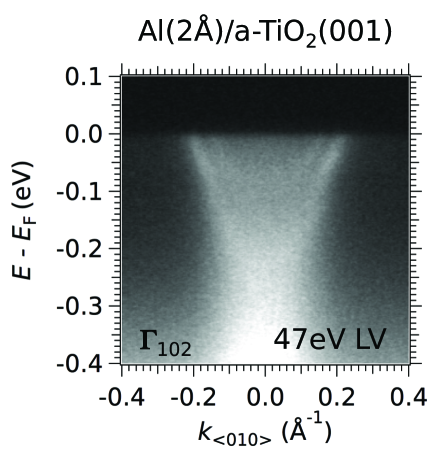
Figure 7 presents the ARPES energy-momentum intensity map at the Al(2Å)/a-TiO2(001) interface. The two subbands form the circular Fermi surfaces shown in Figure 1(f) of the main text. As mentioned there, these Fermi surfaces are almost twice larger than their counterparts at the surface of anatase reduced by photons [26]. In agreement with this observation, the two subbands at the Al(2Å)/a-TiO2(001) interface disperse down to larger binding energies: approximately meV and meV for the upper and lower subbands, respectively, while at the bare, reduced anatase surface they disperse only down to about meV and meV [26].
Oxygen vacancy distribution at the Al(2Å)/anatase interface
The redox reaction creates oxygen vacancies at the Al(2Å)/oxide interface.
The spatial distribution of these electron donors results in the creation of a potential well
confining the electrons and forming the 2DES.
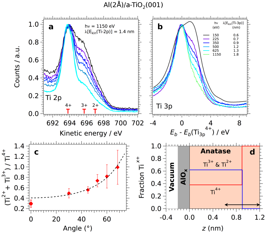
To determine the distribution of vacancies,
we measured the Ti- and Ti- core levels of anatase
using X-ray photoemission at eV as a function of the electron emission angle,
and at normal emission as a function of the X-ray photon energy,
and fitted the peaks using either Voigt or Lorentzian line shapes together with a Shirley background.
As can be seen in Figures S8(a, b),
the core levels are composed of several peaks (red markers)
corresponding to Ti ions of different oxidation state (, , and )
due to the presence of oxygen vacancies.
We observe that the fraction of Ti- of stoichiometric, insulating TiO2
increases for larger electron escape depths, as evidenced
by the angle and photon energy dependencies in Figures S8(a, b).
By contrats, the Ti- and Ti- components,
associated to free carriers and oxygen vacancies,
become increasingly important for smaller escape depths and thus, closer to the interface.
To obtain the concentration profile of the species
along the confinement direction perpendicular to the surface,
we calculate the total area of the corresponding core level peak by:
where is the distance travelled by a photo-emitted electron inside matter
(i.e., anatase AlOx layer), which depends on the emission angle,
and the inelastic mean free path for electrons photo-emitted with kinetic energy .
Figure 8(c) shows the ratio
as a function of the electron emission angle.
The error bars indicate the variation of this ratio
using different line shapes and backgrounds to fit the various Ti peaks.
We then fit the observed changes in such peak area ratio using a Heavyside function
for the concentration profile of oxygen vacancies, as shown in Figure 8(d).
The result of the fit, shown by the dashed curve in Figure 8(c),
yields a depth of Å for the vacancy-rich layer below the surface,
and a fraction of % of Ti ions with oxidation states or .
In-plane and out-of-plane Fermi surfaces of the 2DES in BaTiO3
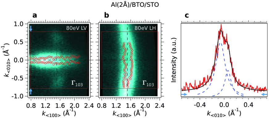
Figures S9(a, b) show the Fermi-surface strips formed by the heavy bands of the 2DES at the surface of BaTiO3 (Al(2Å)/BTO/Nb:STO interface). The data were taken on the same Brillouin zone using mutually orthogonal photon polarizations, which due to photoemission selection rules enhance either the Fermi strip parallel to or the Fermi strip parallel to . The open red circles show the Fermi momenta obtained from Lorentzian fits to the MDCs at . Figure 9(c) shows one of such MDCs, corresponding to a cut at the left edge of the Brillouin zone (light blue arrows). This MDC clearly shows a double-peak structure, corresponding to the two Fermi sheets of the Fermi strip, which is thus open at the Brillouin-zone edge. This is in agreement with the fact that the heavy bands running along the and directions do not cross , as shown in Figures 3(d, e) of the main text. From these MDC fits, the average distance between opposite Fermi momenta along the short side of the Fermi strips is Å-1.
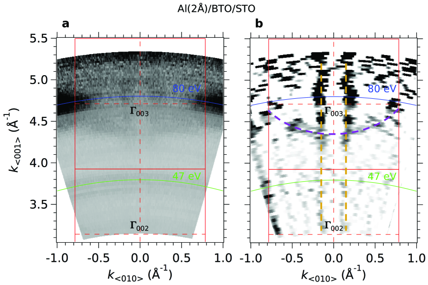
Finally, Figures S10(a, b) show the out-of-plane Fermi-surface map of the 2DES at the surface of BaTiO3, obtained from the photon-energy dependence of the electronic structure measured over more than an entire bulk Brillouin zone. The inner cylinder, yellow dashed lines in Figure 10(b), is associated to the light -like band forming the Fermi circle in the plane. As its Fermi surface does not disperse along the confinement direction, it corresponds to a 2D-like state. The data also show a large ellipse dispersing along , hence presenting a 3D-like character, best seen in the lower part of the Brillouin zone, purple dashed lines in Figure 10(b). This Fermi sheet is associated to the heavy bands forming the Fermi strips in the plane. Of course, such 3D-like behavior cannot correspond to a true bulk state, as the redox reaction occurs only at the interface region. Note also that the 3D carrier density resulting from such a state would be huge, comparable to that of good metals, while the bulk BTO film is still insulating. Instead, such 2D-3D dichotomy between different states forming the 2DES in BaTiO3, also observed for the 2DES at the surface of SrTiO3 [31], can be qualitatively understood as arising from confinement itself. In the bulk, by cubic symmetry, the bands are expected to form 3 identical mutually orthogonal Fermi surfaces similar to prolate ellipsoids along the main crystallographic axes –or open quasi-cylinders, when the band filling is such that the ellipsoids’ long axis extends beyond the zone boundary. Confinement along will result, by Heisenberg’s principle, in “de-confinement”, or elongation, of the ellipsoids along . When the confinement length becomes (one unit cell), the ellipsoid stretches over (one Brillouin zone), and the out-of-plane Fermi surface becomes a cylinder.
Thus, in the case of the 2DES at the surface of BaTiO3, we see from Figure 9 that the Fermi-surface strip formed by -like states has an in-plane Fermi momentum Å-1, while from Figure 10 its out-of-plane Fermi momentum is approximately 0.4 Å-1. Hence, there is an elongation along of the ellipsoids due to confinement. Similarly, as noted before, the in-plane circular Fermi surface, formed by -like states, forms a cylinder along the out-of-plane direction. We then conclude that the planar -like states are more tightly confined to the surface, while the non-planar -like states extend over multiple unit cells towards the bulk. This situation is wholly similar to the case of the 2DES at the surface of SrTiO3 [31], and simply reflects the fact that the confinement potential is wedge-shaped, such that electrons with a large effective mass along ( states) are more confined than electrons with a small effective mass along ( states) [19, 31].
References
- [1] A. Ohtomo, H.Y. Hwang, Nature 2004, 427, 423.
- [2] S. Thiel, G. Hammerl, A. Schmehl, C.W. Schneider, J. Mannhart, Science 2006, 313, 1942.
- [3] N. Reyren, S. Thiel, A.D. Caviglia, L. Fitting Kourkoutis, G. Hammerl, C. Richter, C.W. Schneider, T. Kopp, A.-S. Rüetschi, D. Jaccard, M. Gabay, D.A. Muller, J.-M. Triscone, J. Mannhart, Science 2007, 317, 1196.
- [4] A.D. Caviglia, S. Gariglio, N. Reyren, D. Jaccard, T. Schneider, M. Gabay, S. Thiel, G. Hammerl, J. Mannhart, J.-M. Triscone, Nature 2008, 456, 642.
- [5] A. Brinkman, M. Huijben, M. van Zalk, J. Huijben, U. Zeitler, J.C. Maan, W.G. van der Wiel, G. Rijnders, D.H.A. Blank, H. Hilgenkamp, Nature Mater. 2007, 6, 493.
- [6] L. Li, C. Richter, J. Mannhart, R.C. Ashoori, Nature Phys. 2011, 7, 762.
- [7] J.A. Bert, B. Kalisky, C. Bell, M. Kim, Y. Hikita, H.Y. Hwang, K.A. Moler, Nature Phys. 2011, 7, 767.
- [8] A.D. Caviglia, M. Gabay, S. Gariglio, N. Reyren, C. Cancellieri, J.M. Triscone, Phys. Rev. Lett. 2010, 104, 126803.
- [9] M. Ben Shalom, A. Ron, A. Palevski, Y. Dagan, Phys. Rev. Lett. 2010, 105, 206401.
- [10] Santander-Syro, A.F. et al. A.F. Santander-Syro, F. Fortuna, C. Bareille, T.C. Rödel, G. Landolt, N.C. Plumb, J.H. Dil, M. Radovic, Nat. Mater. 2014, 13, 1085.
- [11] H. Takagi, H. Y. Hwang, Science 2010, 327, 1601.
- [12] J. Mannhart, D.G. Schlom, Science 2010, 327, 1607.
- [13] H.Y. Hwang, Y. Iwasa, M. Kawasaki, B. Keimer, N. Nagaosa, Y. Tokura, Nature Mater. 2012, 11, 103.
- [14] N. Nakagawa, H.Y. Hwang, D.A. Muller, Nature Mater. 2006, 5, 204.
- [15] Y.Z. Chen, N. Pryds, J.E. Kleibeuker, G. Koster, J. Sun, E. Stamate, B. Shen, G. Rijnders, S. Linderoth, Nano letters 2011 11, 3774.
- [16] S.W. Lee, Y. Liu, J. Heo, R.G. Gordon, Nano letters 2012, 12, 4775.
- [17] J. Delahaye, T. Grenet, Journal of Physics D: Applied Physics 2012, 45, 315301.
- [18] E. Lesne et al. , Nat. Commun. 2014, 5, 4291.
- [19] A.F. Santander-Syro, O. Copie, T. Kondo, F. Fortuna, S. Pailhes, R. Weht, X.G. Qiu, F. Bertran, A. Nicolaou, A. Taleb-Ibrahimi, P. Le Fèvre, G. Herranz, M. Bibes, N. Reyren, Y. Apertet, P. Lecoeur, A. Barthélémy, M.J. Rozenberg, Nature 2011, 469, 189.
- [20] W. Meevasana, P.D.C. King, R.H. He, S.-K. Mo, M. Hashimoto, A. Tamai, P. Songsiriritthigul, F. Baumberger, Z.-X. Shen, Nature Mater. 2011, 10, 114.
- [21] A.F. Santander-Syro, C. Bareille, F. Fortuna, O. Copie, M. Gabay, F. Bertran, A. Taleb-Ibrahimi, P. Le Fèvre, G. Herranz, N. Reyren, M. Bibes, A. Barthélémy, P. Lecoeur, J. Guevara, M.J. Rozenberg, Phys. Rev. B 2012, 86, 121107.
- [22] P.D.C. King, R.H. He, T. Eknapakul, P. Buaphet, S.-K. Mo, Y. Kaneko, S. Harashima, Y. Hikita, M.S. Bahramy, C. Bell, Z. Hussain, Y. Tokura, Z.-X. Shen, H.Y. Hwang, F. Baumberger, W. Meevasana, Phys. Rev. Lett. 2012, 108, 117602.
- [23] C. Bareille, F. Fortuna, T.C. Rödel, F. Bertran, M. Gabay, O. Hijano Cubelos, A. Taleb-Ibrahimi, P. Le Fèvre, M. Bibes, A. Barthélémy, T. Maroutian, P. Lecoeur, M.J. Rozenberg, A.F. Santander-Syro, Scientific Reports 2014, 4, 1.
- [24] T.C. Rödel, C. Bareille, F. Fortuna, C. Baumier, F. Bertran, P. Le Fèvre, M. Gabay, O. Hijano Cubelos, M.J. Rozenberg, T. Maroutian, P. Lecoeur, A.F. Santander-Syro, Phys. Rev. Applied 2014, 1, 051002.
- [25] S. McKeown Walker, A. de la Torre, F.Y. Bruno, A. Tamai, T.K. Kim, M. Hoesch, M. Shi, M.S. Bahramy, F. Baumberger, Phys. Rev. Lett. 2014, 113, 177601.
- [26] T.C. Rödel, F. Fortuna, F. Bertran, M. Gabay, M.J. Rozenberg, A.F. Santander-Syro, P. Le Fèvre, Phys. Rev. B 2015, 92, 041106(R).
- [27] Q. Fu, T. Wagner, Surface Science Reports 2007 62, 431.
- [28] Q. Fu, T. Wagner, The Journal of Physical Chemistry B 2005, 3, 11697.
- [29] S.-I. Kim, D.-H. Kim, Y. Kim, S.Y. Moon, M.-G. Kang, J.K. Choi, H.W. Jang, S.K. Kim, J.-W. Choi, S.-J. Yoon, H.J. Chang, C.-Y. Kang, S. Lee, S.-H. Hong, J.-S. Kim, S.-H. Baek, Adv. Mater. 2013, 25, 4612.
- [30] V.T. Tra, J.-W. Chen, P.-C. Huang, B.-C. Huang, Y. Cao, C.-H. Yeh, H.-J. Liu, E.A. Eliseev, A.N. Morozovska, J.-Y. Lin, Y.-C. Chen, M.-W. Chu, P.-W. Chiu, Y.-P. Chiu, L.-Q. Chen, C.-L. Wu, Y.-H. Chu, Adv. Mater. 2013, 25, 3357.
- [31] N.C. Plumb, M. Salluzzo, E. Razzoli, M. Månsson, M.Falub, J. Krempasky, C.E. Matt, J. Chang, M. Schulte, J. Braun, H. Ebert, J. Minár, B. Delley, K.-J. Zhou, T. Schmitt, M. Shi, J. Mesot, L. Patthey, M. Radovic, Phys. Rev. Lett. 2014 113, 086801.
- [32] P.D.C. King, S. McKeown Walker, A. Tamai, A. de la Torre, T. Eknapakul, P. Buaphet, S.-K. Mo, W. Meevasana, M.S. Bahramy, F. Baumberger, Nature communications 2014, 5, 3414.
- [33] A. Schilling, T.B. Adams, R.M. Bowman, J.M. Gregg, G. Catalan, J.F. Scott, Phys. Rev. B 2006, 74, 024115.
- [34] N.A. Pertsev, A.G. Zembilgotov, A.K. Tagantsev, Phys. Rev. Lett. 1998, 80, 1988.
- [35] K.J. Choi, M. Biegalski, Y.L. Li, A. Sharan, J. Schubert, R. Uecker, P. Reiche, Y.B. Chen, X.Q. Pan, V. Gopalan, L.-Q. Chen, D.G. Schlom, C.B. Eom, K.J. Choi, Science 2004, 306, 1005.
- [36] J. Chen, Y. Luo, X. Ou, G. Yuan, Y. Wang, Y. Yang, J. Yin, Z. Liu, J. Appl. Phys. 2013, 113, 204105.
- [37] S. Goswami, E. Mulazimoglu, L.M.K. Vandersypen, A.D. Caviglia, Nano Lett. 2015, 15, 2627.
- [38] M. Setvín, B. Daniel, V. Mansfeldova, L. Kavan, P. Scheiber, M. Fidler, M. Schmid, U. Diebold, Surface Science, 2014, 626, 61.
- [39] N.P. Guisinger, T.S. Santos, J.R. Guest, T.-Y. Chien, A. Bhattacharya, J.W. Freeland, M. Bode, ACS nano, 2009, 3, 4132.
- [40] N. Cai, G. Zhou, K. Müller, D.E. Starr Phys. Rev. Lett., 2011, 107, 035502.
- [41] G. Berner, M. Sing, H. Fujiwara, A. Yasui, Y. Saitoh, A. Yamasaki, Y. Nishitani, A. Sekiyama, N. Pavlenko, T. Kopp, C. Richter, J. Mannhart, S. Suga, R. Claessen, Phys. Rev. Lett., 2013, 110, 247601.
- [42] M. P. Seah and W. A. Dench, Surface and Interface Analysis, 1979, 1, 2.