Present address :] Physics and Materials Science Research Unit, University of Luxembourg, LIST-Belvaux site, 41 rue du Brill, L-4422 Belvaux, Luxembourg
Corresponding Author :] constance.toulouse@uni.lu
Patterning enhanced tetragonality in BiFeO3 thin films with effective negative pressure by helium implantation
Abstract
Helium implantation in epitaxial thin films is a way to control the out-of-plane deformation independently from the in-plane strain controlled by epitaxy. In particular, implantation by means of a helium microscope allows for local implantation and patterning down to the nanometer resolution, which are of interest for device applications. We present here a study of bismuth ferrite (BiFeO3) films where strain was patterned locally by helium implantation. Our combined Raman, XRD and TEM study shows that the implantation causes an elongation of the BiFeO3 unit cell and ultimately a transition towards the so-called super-tetragonal polymorph via states with mixed phases. In addition, TEM reveals the onset of amorphization at a threshold dose that does not seem to impede the overall increase in tetragonality. The phase transition from the R-like to T-like BiFeO3 appears as first-order in character, with regions of phase coexistence and abrupt changes in lattice parameters.
I Introduction
Strain engineering has arisen in the last decade as an essential means to tune physical properties in functional thin films. The most common way to tune strain in films is by using epitaxial strain, imposing an in-plane biaxial strain to the material due to the lattice misfit with the substrate on which the film is grown. The strain state can be varied by using different substrates, or even in some instances, can be tuned continuously, for example by an electric field applied on a piezoelectric substrateBilani-Zeneli et al. (2008); Dörr et al. (2009); Herklotz et al. (2010). Using this approach, it has been demonstrated that the properties of the films can be controlled and modified, sometimes spectacularly. Remarkable results have included induced ferroelectricityPertsev et al. (2000); Tyunina et al. (2010); Kim (2011); Guo et al. (2018), a modified magnetic ground state of multiferroic compoundsLee and Rabe (2010); Sando et al. (2013); Agbelele et al. (2016) or strain-induced structural transitionsYamada et al. (2010); Schwarzkopf et al. (2012); Mao et al. (2016); Weber et al. (2016). In this classical approach of strain engineering, only the in-plane biaxial strain is controlled; the out-of-plane strain is fixed by the elastic equilibrium of the system, but cannot be controlled independently.
Controlling this additional strain parameter, and in particular achieving an elongation of the unit cell (“negative pressure”), is of high interest. Negative pressure has, indeed, been theoretically predicted to trigger various properties modifications Tinte et al. (2003); Liu et al. (2009); Wang et al. (2015); Kvasov et al. (2016). Experimentally, it can be achieved by helium implantation. Due to its nobility, helium implants interstitially, without chemical substitution, thus inducing a ‘swelling’ of the host material’s unit cell volumeSharma et al. (2017). Helium implantation is customarily achieved by lab ion sources Guo et al. (2015); Herklotz et al. (2016a, b); Guo et al. (2018); Herklotz et al. (2019) similar to the ones used for wafer processing in semiconductor engineering. Another route - the one chosen in the present work - is to use a helium ion microscope as a way to implant ions locally. This technique has recently started to be used as a means of defect engineeringMcGilly et al. (2017); Saremi et al. (2018), but our study is aiming at using a helium microscope for strain-engineering purposes. The interest of this new method lies in particular in the nano-patterning possibilities allowed by the sub-nanometer resolution of the microscopeZeiss (2008). Moreover, it has been demonstrated recently that helium implantation is a reversible process and that the helium trapped can be released with annealing at high temperatures above and under oxygen atmosphereGuo et al. (2015), allowing for reversible properties tuning. For instance, a very recent study on FeRh thin films shows that local helium implantation allows for direct writing of nanoscale domains with a metamagnetic order tunable with the implanted dose, demonstrating the application potential of this techniqueCress et al. (2020).
Here, we demonstrate the use of a helium ion microscope to perform strain engineering by helium implantation on bismuth ferrite (BiFeO3) thin films. BiFeO3 is one of the most studied multiferroic compounds as it exhibits multiferroicity well above room temperature. In its bulk form it develops below a very large ferroelectric polarization Lebeugle et al. (2007) () along the direction of its pseudo-cubic structure and exhibits below a G-type antiferromagnetic ordering of the iron spins with a superimposed long range cycloidal modulation in a plane containing the ferroelectric local mode vectorWang et al. (2003). In its thin film form, BiFeO3 undergoes a structural transition under epitaxial strain. At low strain, it crystallizes in a so-called R-phase in the monoclinic structure, slightly distorted from the bulk rhombohedral structure in the R3c space group. At high strain or under certain growth conditions, BiFeO3 can exhibit a structural phase with enhanced tetragonality (with a ratio between 1.22 and 1.25) in the monoclinic structure, called the super-tetragonal or T-phase in which an enhanced ferroelectric polarization has been observed and theoretically reproducedSando et al. (2016). Many studies report the existence of intermediate mixed R-T phases in BiFeO3 films, with a 3 tilt of the monoclinic angle between the phasesSando et al. (2014). Regarding functional properties, epitaxial strain has been shown to modify the ferroic properties of BiFeO3 films: the ferroelectric Curie transition temperature is decreased under epitaxial strain Infante et al. (2010) while the bulk-like magnetic cycloid present at low strain is destroyed at high epitaxial strain, both tensile and compressive, leaving place to a canted antiferromagnetic state Sando et al. (2013); Agbelele et al. (2016).
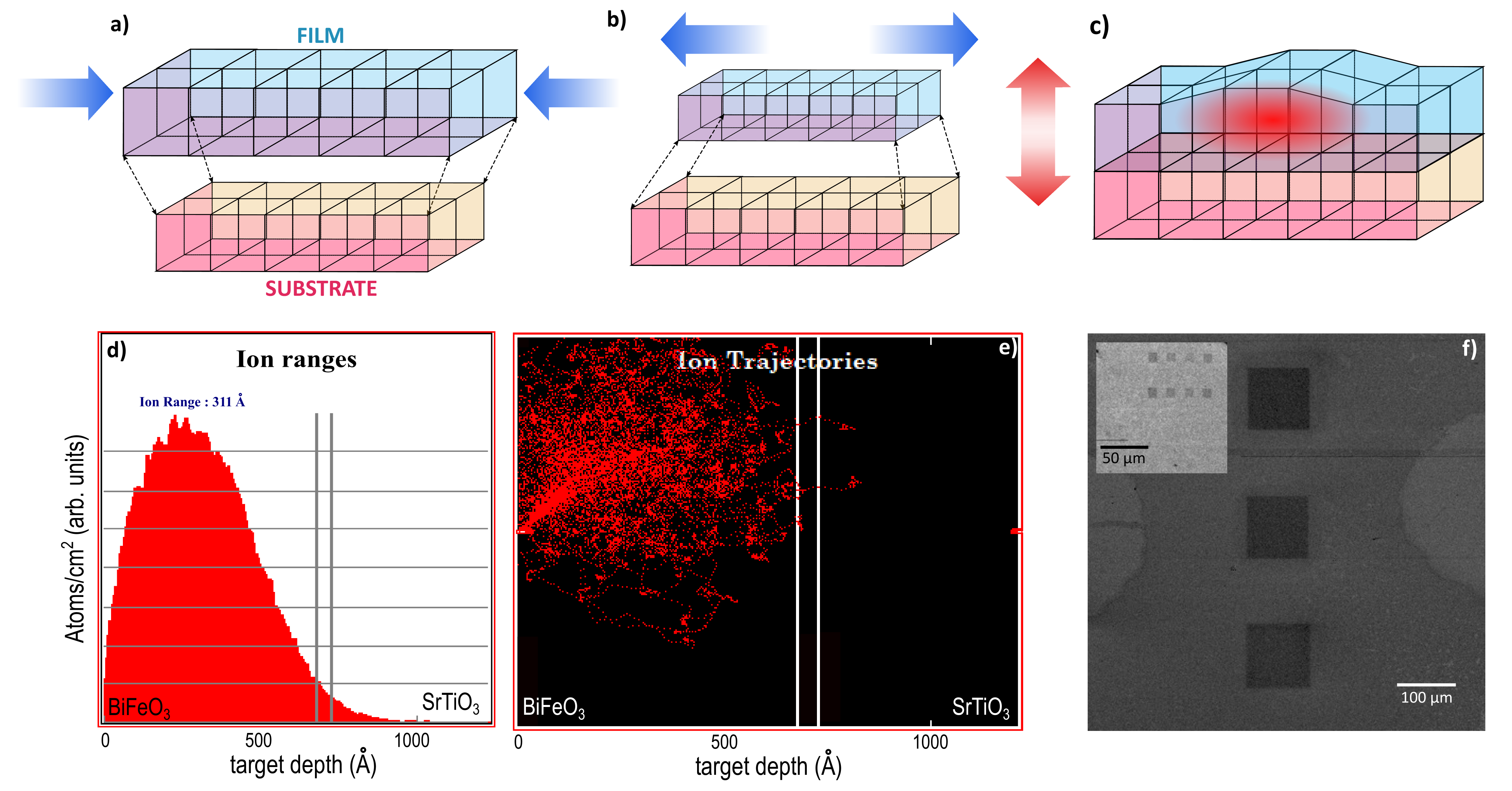
Relying on the interplay between epitaxial strain and helium implantation, a full tridimensional control of strain in thin films can be achieved. The lattice misfit between the substrate and the film’s native bulk compound causes a biaxial strain in the plane of epitaxy (Fig 1.a and 1.b). Due to the in-plane clamping of the film to its substrate, helium implantation gives rise to an out-of-plane negative pressure, without modification in-plane (Fig 1.c). In the case of BiFeO3 thin films, helium implantation allows to trigger the transition towards the super-tetragonal phase, by enhancing tetragonality due to this out-of-plane strain tuning. It has been shown recently that large scale helium implantation on epitaxial BiFeO3 films can induce the super-tetragonal phase on LSAT substrate, while enhancing tetragonality in R-like and T-like films grown on SrTiO3 and LaAlO3 respectivelyHerklotz et al. (2019). This raises important questions regarding the the transition from the R-like to T-like structure, here caused by continuously varying the helium dose: character of the transition, possibility of coexistence between the two phases, presence of interfaces, etc. Here, by combining local and non-local probes, we bring insight on the mechanism of this R to T structural transition under helium implantation, that appears first order in character. In addition, we show that local helium implantation allows to pattern the tetragonality of the structure while preserving crystal quality, demonstrating the possibility to structurally pattern BiFeO3 films.
II Experimental details
BiFeO3 epitaxial films were grown by pulsed laser deposition on oriented SrTiO3 (-1.5 % lattice misfit with BiFeO3) and DyScO3 (-0.4 % lattice misfit) substrates with a thick SrRuO3 bottom electrode as described in refs [Farokhipoor and Noheda, 2011; Farokhipoor and Noheda, 2012; Haykal et al., 2020]. The thickness of the films was set to . For the film grown on DyScO3, this is thin enough to avoid strain relaxation, while for the film grown on SrTiO3, the formation of in-plane ferroelastic 71 domains induce partial strain relaxation already at thickness, but their alternation allows for overall epitaxial matching with the substrateDaumont et al. (2010).
Helium implantation of our films was performed using an Orion NanoFab helium ion microscope (HIM) Wirtz et al. (2019). Various doses of 6 keV helium ions were implanted into square regions with sizes ranging from to (Fig. 1.f). We kept the doses below 11016 ions cm-2, which, at the energy used, is below the threshold for structural defect formation Livengood et al. (2009); Autier-Laurent et al. (2010); Wei et al. (2012). The implantation parameters, in particular the beam energy and the impact angle, were determined by SRIMZiegler (2004) (Stopping Range of Ions in Matter) and TRIM (TRansport of Ions in Matter) simulations in order to have the maximum of the implantation profile inside the film (Fig. 1.d,e). The samples were therefore tilted 49 from the normal to reduce helium implantation of the bottom electrode and the substrate while also avoiding channeling through the crystal structure’s easy planes. The TRIM simulations of the implanted ion distribution and depth profile taking density values of for BiFeO3, for SrRuO3 and of for SrTiO3 as taken from the literatureSchneeloch et al. (2015); noa (2019) are shown on Fig. 1.d and 1.e.
To probe our implanted samples, we used Raman spectroscopy, electron microscopy and X-ray diffraction (XRD) techniques. Micro-Raman measurements were performed with a He-Cd laser in an inVia Renishaw micro-Raman spectrometer. Depth profiles were acquired by varying the focus, meaning the distance between the objective and the sample, with steps. Principle Components Analysis (PCA) and Non-negative Matrix Factorization (NMF), using the R-DATA software as described in Ref. [Schober et al., 2020], allow to extract the layer’s signal from the overall substrate’s contribution.
Transmission Electron Microscopy (TEM) studies of cross-sectional samples were performed in a probe corrected FEI Titan3 G2 60-300, working at in scanning mode (STEM) using a High Angle Annular Dark-Field detector (HAADF). The microscope is equipped with a Bruker Super-X Energy-Dispersive X-ray spectroscope (EDX), used for obtaining elemental maps. Geometrical Phase Analysis (GPA)Hÿtch et al. (1998) using Strain++ software, was applied on atomically resolved HAADF images in order to measure local deformations of the lattice.
The XRD synchrotron data were collected at two different synchrotron sources. Diffracted intensity maps were recorded at the ID03 Surface Diffraction beamline of the ESRF using the 6-circle vertical diffractometer. The experiment was conducted using an incident wavelenght of 0.516 Å (24 keV) and a beamsize of (horizontal vertical). For the grazing incidence experiments, an incidence angle of 3 degrees was used and allowed to produce a beam footprint on the sample surface with a size comparable to the area of the implanted region. The implanted region was aligned in the beam using a camera with a macro lense and the visible fluorescence of the sample under the x-ray beam irradiation. The data were collected using a Maxipix pixel detector and processed using the BINoculars code. At the CRISTAL Beamline of SOLEIL Synchrotron, we performed localized XRD measurements on a 6-circle diffractometer, using a beam size of ), with an imXpad pixel detector and a wavelength of . The implanted regions could be localized easily, due to their different 00l XRD signal, by scanning the sample spatially. All the diffraction data are reported using the substrate lattices as reference systems.
III Results and discussion
III.1 Raman spectroscopy
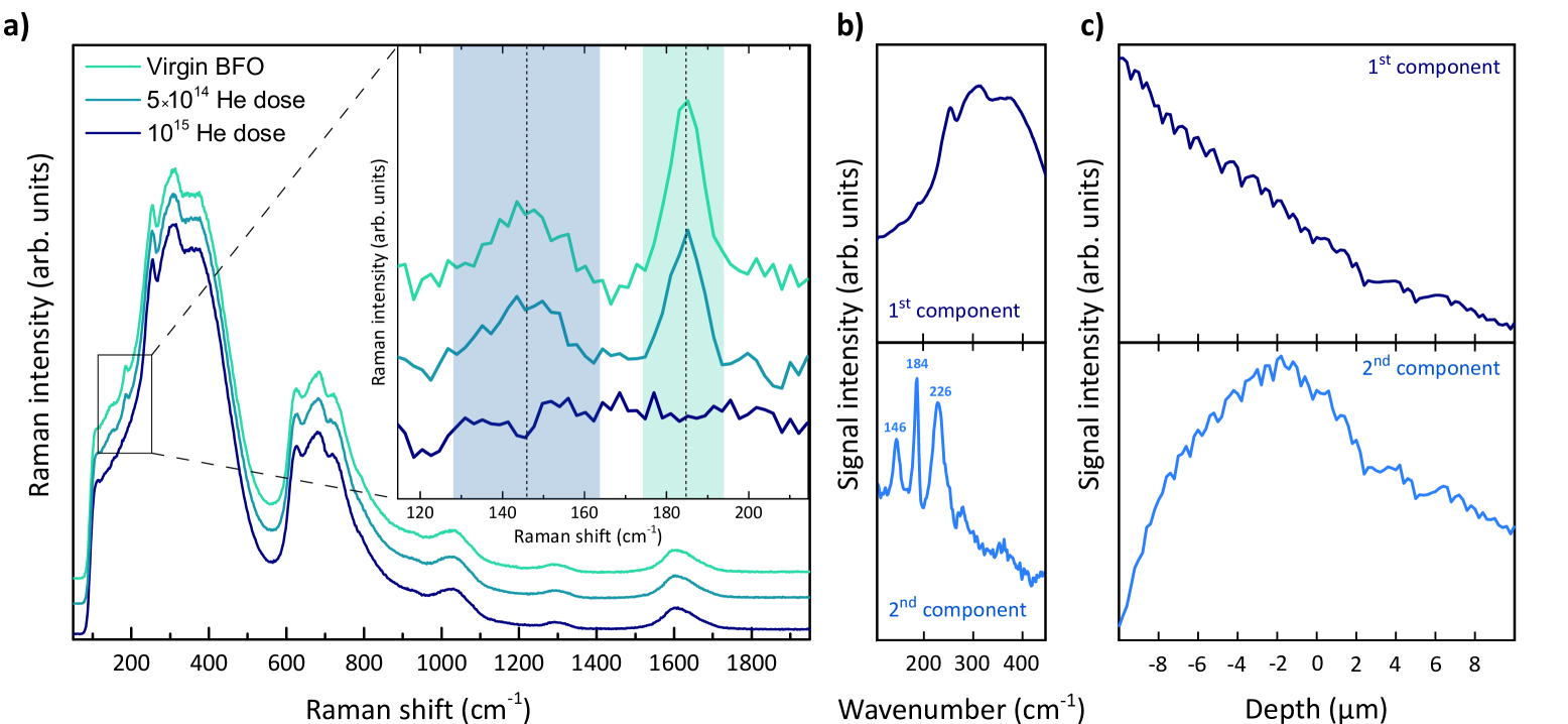
Raman spectroscopy measurements have been performed on our implanted samples to study the effect of implantation on the lattice via the phonon modes. Thin films make it naturally increasingly difficult to single out the signal of the film from the substrate contribution. However, due to the broad peaks of Raman signal of SrTiO3, some sharper Raman modes from the BiFeO3 layer were possible to observe in our BiFeO3//SrTiO3 sample. Raman spectra measured on regions with different doses are shown in Fig. 2.a. Two low energy phonon modes can be seen emerging from the substrate’s signal at 146 and 184 cm-1. These phonon modes correspond to Raman excitations with symmetry, usually measured around 145-147 and 176-180 cm-1 respectivelyFukumura et al. (2007); Cazayous et al. (2007).
Furthermore, we performed Raman depth profiles by continuously varying the distance between the sample and the Raman objective, following the approach described in Ref. [Schober et al., 2020]. Fig. 2.b and Fig. 2.c, present the Principal Component Analysis (PCA) of the Raman signal obtained on the non-implanted part of the film. Fig. 2.b shows the signal associated to the first two components while Fig.2.c shows their intensity profile as a function of the depth. The first component of the PCA visibly corresponds to the SrTiO3 signal: it has the same shape than the well-known SrTiO3 2nd-order Raman signal (Fig. 2.b, top) while its intensity continuously increases when the distance between the sample and the objective decreases (Fig 2.c, top). This is in agreement with the signal coming from the substrate, further away from the objective. The second component of the PCA presents a signal where 3 narrow peaks can be observed at 146, 184 and 226 cm-1 (Fig. 2.b, bottom). These peaks corresponds to the two BiFeO3 Raman modes observed in the spectra of Fig. 2.a, with an additional peak at 226 cm-1 also associated to an Raman mode of BiFeO3 in the literatureFukumura et al. (2007); Cazayous et al. (2007). The intensity depth profile of this second component presents a maximum in the depth range corresponding to the film (Fig. 2.c, bottom) which confirms that we can indeed attribute it to the Raman signal of the BiFeO3 film.
By comparing the evolution of the Raman signal with the implanted helium dose, we observe that the Raman signal of the BiFeO3 film disappears with increasing dose while not shifting in frequency. Indeed, the two phonon modes are visible only for the virgin film and the lowest dose (51014 He cm-2, Fig. 2.a). The Raman spectrum of BiFeO3 could not be seen for the films deposited on DyScO3 substrate, due to a stronger substrate contribution.
Several causes can be envisioned to explain the disappearance of the Raman signal. In the context of BiFeO3 in particular, the Raman signal of the super-tetragonal phase is weaker by one order of magnitude than the signal for the rhombohedral-like structure Iliev et al. (2010). The disappearance of the Raman signal under implantation can therefore be a signature of a transition towards an increased tetragonality, as we would expect (cf. Fig. 1.c and Ref. [Herklotz et al., 2019]). Alternatively, a vanishing Raman spectrum can be associated to a transition towards a metallic character, which in BiFeO3 is known to happen at very high temperatures and pressure. In this particular context, it is also conceivable that an increase in band gap i.e. a decrease in absorption would lead to a decrease in intensity of the Raman spectrum as compared to the substrate. Finally, we cannot exclude an effect directly due to the presence of He in the BiFeO3 lattice, decreasing the Raman intensity.
III.2 Transmission Electron Microscopy
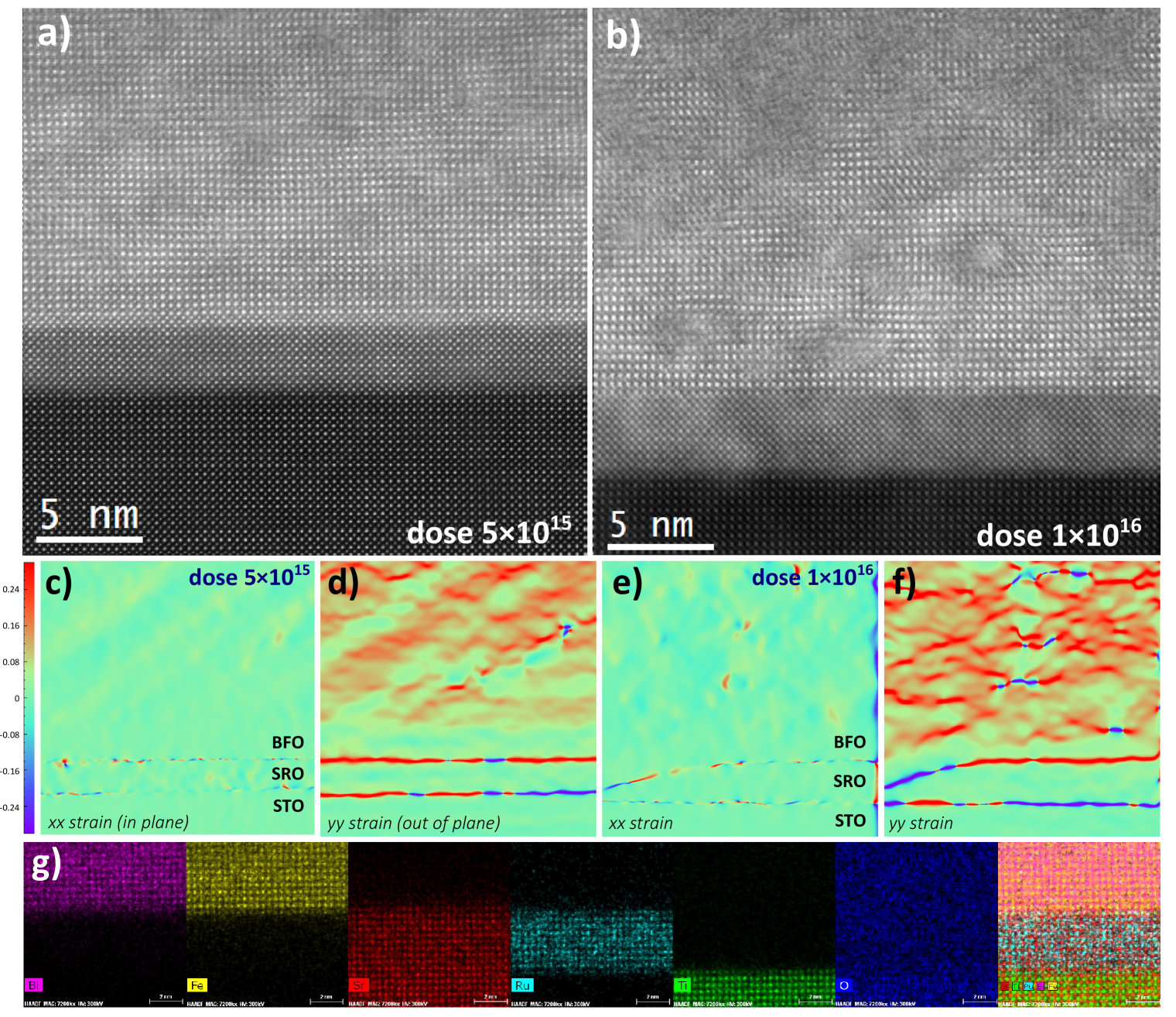
To gain more insight on the effect of implantation at the local scale, Transmission Electron Microscopy was performed on prepared samples from a BiFeO3 layer grown on a SrTiO3 (001) substrate, with doses 51015 and 11016 He cm-2.
The High-Angle Annular Dark Field (HAADF) STEM images of the BiFeO3/SrTiO3 interfaces, in the two implanted regions are shown on Fig. 3.a and 3.b. No amorphization of the BiFeO3 layer is visible under implantation for the region with 51015 He cm-2 dose : the epitaxial columns are clearly visible throughout the film although some structural defects are present (as expected under implantation). When the implanted dose is increased to a higher level, however, some regions of amorphization are observed (Fig. 3.b). Their characteristic size is of the order of the nanometer, and is reminiscent of the observation of defect “nano-bubbles” previously reported upon He implantation on silicon Livengood et al. (2009).
To gain insight on the strain induced locally by helium implantation, Geometric Phase Analysis (GPA) has been performed on samples prepared with 51015 and 11016 He cm-2 doses, taking as a reference the SrTiO3 lattice to extract local deformations. We see in Fig. 3.c and 3.e the in-plane strain for both doses, while the out-of-plane strain is shown on Fig. 3.d and 3.f. While it is apparent from the GPA strain maps that local deformations in-plane are very small, we observe stronger out-of-plane deformations, consistent with an out-of-plane swelling induced by implantation. The strain seems to increase with the dose between Fig. 3.d and 3.f, as expected for an enhanced tetragonality.
Furthermore, we extracted the average lattice parameters by performing Fourier transform of the STEM images in the two regions with 51015 and 11016 He cm-2 doses as well as in a pristine -non-implanted- region as a reference. They are given in Table 1. Each lattice parameter was estimated from 10 images and the error bars arise from the standard deviation of the measurements. We can clearly see that the in-plane lattice parameter remains unchanged while a c-lattice expansion, increasing with the helium dose, is observed with implantation. Moreover, we can observe that in the region implanted with the highest dose, the c-axis lattice parameter extracted by Fourier transform has a much broader error bar, consistent with a loss of crystallinity of the film as visible from Fig. 3.b.
| Sample | a | c | c/aSTO |
|---|---|---|---|
| STO substrate | 3.79 | 3.92 | |
| BFO pristine | 3.82 | 4.02 | 1.03 |
| BFO (51015 He cm-2) | 3.79 | 4.38 | 1.12 |
| BFO (11016 He cm-2) | 3.78 | 4.57 | 1.17 |
Finally, Energy Dispersive X-Ray Spectroscopy (EDX) chemical analysis of the atoms at the interface between the substrate and the film (with a thick SrRuO3 bottom electrode) has been performed and is presented in Fig. 3.g. The chemical compositions of the substrate, the bottom electrode and the layer are well resolved and the compositional interfaces correspond to those of the HAADF image with no indication of chemical intermixing. Furthermore, no migration of the atoms of the layer to the bottom electrode or substrate is observed under implantation.
III.3 Synchrotron XRD
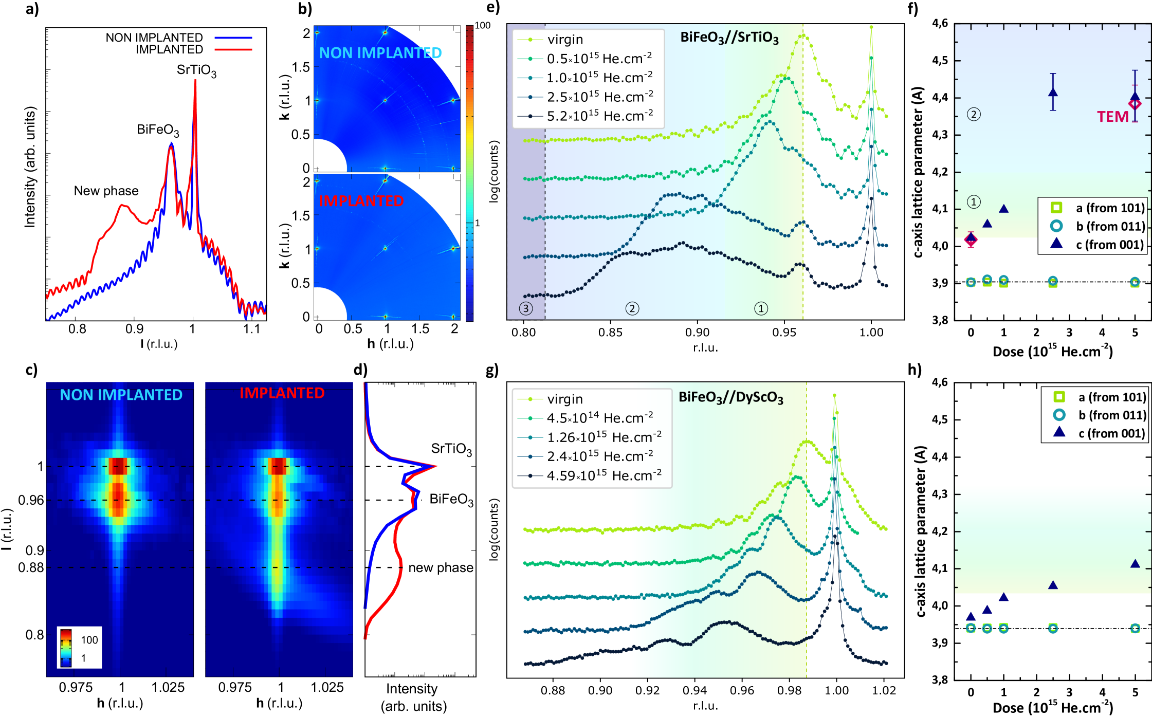
To determine the effect of helium implantation on the structure of our BiFeO3 layers, we performed micro-XRD, using specular reflectivity and grazing incidence geometry. Fig. 4.a shows the specular reflectivity curve measured inside an implanted region (with 51015 He cm-2 dose) on a BiFeO3 film grown on SrTiO3 substrate. It shows, in addition to the (001) Bragg peaks of the SrTiO3 substrate and the BiFeO3 layer, a new phase with a -lattice expansion, revealed by the new peak appearing at l=0.89 r.l.u (Fig. 4.a).
From the in-plane diffracted intensity maps measured at different l values it was possible to verify that all the phases have the same in-plane lattice parameters of the substrate, as observed locally from the TEM results. A comparison between the hk maps collected at l=0.96 for the implanted and non-implanted regions (Fig. 4.b) shows no difference in the positions of the BiFeO3 Bragg peaks, indicating no modification of the in-plane lattice parameter as a consequence of the implantation process: as expected, the clamping to the substrate locks the film parameters in the epitaxial plane. Fig. 4.c shows the hl maps around the (001) Bragg peak of the SrTiO3 substrate outside and inside an implanted region (with 51015 He cm-2 dose). The peak of the substrate and, at lower l, of the BiFeO3 layer, are clearly visible while a new phase, with a -lattice expansion of 7.9% (from 4.072 to ) is observed in the implanted region, consistent with the values extracted from the TEM images. Fig. 4.d shows a close-up of the (10l) rod around the (001) region, in which the coexistence of the new structural phase and the pristine BiFeO3 layer are visible. This can be explained by a mixing of the two structural phases, the pristine R-like phase and the new phase with enhanced tetragonality in the implanted region. Alternatively, the R-type signal could also arise from neighboring non-implanted regions, partly probed due to the X-ray spot size that was slightly larger than the implanted region.
In order to study the conditions of appearance of this new phase under helium implantation, we performed implantations with increasing doses. The XRD scans, around the Bragg peak of the SrTiO3 substrate for doses ranging between 51014 and 51015 He cm-2 are shown on Fig. 4.e. We observe the peak of the BiFeO3 layer progressively shifting towards higher -axis lattice parameters with dose. Under 2.51015 He cm-2 (region \raisebox{-.9pt}{1}⃝, in green Fig. 4.e), the layer’s (001) peak shifts continuously. At 2.51015 He cm-2, however, we observe an abrupt change in the (001) Bragg signal of the layer (region \raisebox{-.9pt}{2}⃝, in blue Fig. 4.e), with a strong shift of the layer peak, that we interpret as the appearance of the new phase previously observed in Fig. 4.c,d and the onset of the R-like to T-like BiFeO3 structural transition. In this new phase (at 2.51015 He cm-2 dose and above), we also observe the presence of a peak at the position of the peak of the virgin (non-implanted) BiFeO3 layer, as observed in Fig. 4.c,d. In this measurement, the spot size was well below the size of the implanted regions and its centering by means of (x,y) scans ruled out the possibility of signal coming from non-implanted BiFeO3. The presence of the pristine-like BiFeO3 peak therefore unambiguously points to a phase mixture in the implanted region.
The lattice parameters were extracted directly from the , and XRD peaks of the film in the different regions. They are shown, as a function of the implanted helium dose, in Fig. 4.f, the dotted line marking the lattice parameter of the SrTiO3 cubic substrate. As observed previously, the in-plane lattice parameters are not modified under implantation.
To investigate the combined effect of epitaxial strain and implantation, we performed implantations with the same helium doses on a film synthesized on a DyScO3 susbtrate, which has a lattice parameter closer to BiFeO3 (-0.4 % lattice misfitHaykal et al. (2020)). Fig. 4.g shows the XRD scans, around the Bragg peak of the DyScO3 substrate for doses ranging between 51014 and 51015 He cm-2. We see the peak of the BiFeO3 layer progressively shifting with dose, showing an increase of the out-of-plane lattice parameter. Contrary to the results on the SrTiO3 substrate, no abrupt modification is observed and the lattice parameter (reported in Fig. 4.h) is in the same range than in the \raisebox{-.9pt}{1}⃝ region of the Fig. 4.f on the SrTiO3 sample. This indicates a strained R-like structure with no phase transition. As on SrTiO3, we observe no modification of the in-plane and lattice parameters, locked by the DyScO3 lattice parameter (dotted line, Fig. 4.h).
III.4 Discussion
By combining Raman spectroscopy, electron microscopy and X-ray diffraction, we could access the structural changes due to implantation at different length scales, allowing for a more complete insight into the transition between the rhombohedral and super-tetragonal phases of BiFeO3 films than previously reported. Specifically, helium implantation is a way to observe the transition with a continuously varying parameter, as opposed to epitaxial strain that typically takes only a few discrete values fixed by the substrates.
Our TEM measurements, in particular, clearly show both the elongation of the unit cell and the partial amorphization. We indeed observe amorphized regions at 11016 He cm-2 dose, while at the same time, the c-axis lattice parameter extracted by Fourier transform from the non-amorphized regions present a ratio with the a-axis lattice parameter which is close to the ratio of the super-tetragonal phaseSando et al. (2016). It therefore seems that despite the structural damage due to the loss of crystallinity of some regions, we continue to enhance the tetragonality of the still crystalline regions of the film, towards the T-phase. It is not possible to know if amorphization was also present in the previous study on He-implantation of BiFeO3 films using a large scale ion implantorHerklotz et al. (2019) as XRD is only sensitive to the crystalline regions. In our XRD data, where the dose was kept low enough to avoid amorphization, the elongation of the unit cell does not reach the typical of the super-tetragonal phase. Whether or not it is possible to fully transform into the super-tetragonal phase on SrTiO3 while remaining fully crystalline, is still to be investigated.
The picture provided by our TEM and XRD data shows significant differences when compared to the same phase transition reported in Ref. Herklotz et al., 2019 on (LaAlO3)0.3(Sr2TaAlO6)0.7 (LSAT) and SrTiO3. We observe the transition towards a mixed phase with an enhanced tetragonality both at lower epitaxial strain and at lower doses: Herklotz et al.Herklotz et al. (2019) observe a structural transition towards the T phase on LSAT, with a -2.6% lattice misfit and a 61015 He cm-2 dose, whereas we already see a similar behaviour with enhanced tetragonality on SrTiO3 where the lattice misfit is only -1.5% at a 2.51015 He cm-2 dose. These discrepancies are not negligible, and their origin is for the moment unclear. They could be due to an inaccurate estimation of the implanted dose or to a different local behaviour, resulting in a strain gradient, that may be due to the difference in implantation technique. In particular, the presence of interfaces between implanted and non-implanted regions, specific to the patterning possibilities of our implantation technique, can impact the strain relaxation mechanisms and account for a higher applied strain with respect to the dose as compared to large scale implantation techniques. Moreover, the thickness and possible domain structure differences can give rise to different stress field landscapes, that may account for the differences in our study. Furthermore, the energy of the accelerated He ions with the He-FIB we use is higher than with a large scale ion implanter as used in Ref. [Herklotz et al., 2019]. Special attention should be paid to these aspects in future studies.
A noticeable difference also lies in the way the transition proceeds with increasing dose. In Ref. [Herklotz et al., 2019], the transition is described as appearing continuously under implantation with a progressive shift of the Bragg peak (cf. Fig. 1.b of the Ref. [Herklotz et al., 2019] for the film grown on LSAT). They further support the scenario of a continuously rotating polarization based on PFM and SHG observations. In our measurements, in contrast, the emergence of the T-like phase appear the be step-like with a visible phase coexistence, reminiscent of a first-order transition. We believe this is not, in fact, incompatible with their raw XRD data, where a splitting of the Bragg peak can be seen at intermediate doses. We hypothesize that the continuous character observed in PFM and SHG could result from an averaging effect that does not reflect the details of the local picture.
Finally, the comparison between Raman and XRD data sheds light on the disappearance of the Raman spectrum. We can see that the Raman signal disappears at a dose (11015 He cm-1) where the BiFeO3 is still clearly in a slightly elongated R phase. Indeed, the XRD scan (Fig. 4.e) still shows a narrow 001 Bragg peak, shifted from the pristine BiFeO3, but still showing no sign of transition from the rhombohedral-like structure. Therefore, the vanishing of the Raman signal cannot be attributed to the lower Raman intensity known for the T phase, and cannot be understood as a signature of the transition towards the tetragonal-like structure. Instead, we suggest that it reflects a decrease of Raman susceptibility and polarizability due to the insertion of helium ions. This might be significant also for the dielectric properties of the implanted films.
IV Conclusion
Helium implantation has arisen recently as a powerful technique with the potential to modify and tune the strain state in a perovskite film. We have shown here, in particular, that local helium implantation by means of a helium ion microscope can enhance tetragonality in (001)-oriented BiFeO3 thin films, increasing the out-of-plane lattice parameter up to 4% in films grown on DyScO3 and up to 9% in films grown on SrTiO3, inducing locally a structural phase transition towards a mixed R-T phase.
Combined Raman spectroscopy, electron microscopy and X-Ray diffraction measurements allowed us to probe the structural changes both at the large scale and locally. Our local (TEM) study allowed us to determine the threshold dose for which amorphization starts to appear in implanted regions, while observing elongations of the unit cell along the c-axis up to the values nearing the super-tetragonal lattice distortion. Synchrotron XRD performed in the locally implanted regions allowed us to probe the onset of the transition between the rhombohedral-like structure and the super-tetragonal phase. Our data suggest that this transition appears as a first-order transition, with an abrupt jump of the c-axis expansion at a threshold dose (2.51015 He cm-1 on SrTiO3), which opens the discussion for understanding the underlying mechanisms at stake in this structural transition under implantation.
More generally, this work demonstrates the use of a helium microscope as a powerful mean for strain-engineering by local helium implantation and opens technical possibilities for property tuning and patterning.
Acknowledgments
This work was supported by the Fond National de la Recherche (FNR) of Luxembourg (PEARL CO-FERMAT, Project code FNR/P12/4853155/Kreisel). We acknowledge SOLEIL for provision of synchrotron radiation at CRISTAL beamline (proposal number 20190831). TEM sample preparation and observation was carried out within the MATMECA consortium and supported by the ANR under contract number ANR-10-EQPX-37. It has benefited from the facilities of the Laboratory MSSMat, CNRS, CentraleSupélec, Université Paris-Saclay, France. The author Inma Peral is supported by the National Research Fund of Luxembourg (Grant No FNR-Inter2015/LRSF). Saeedeh Farokhipoor acknowledges financial support from a VENI grant (016.veni.179.053) of the Netherlands Organisation for Scientific Research (NWO).
References
- Bilani-Zeneli et al. (2008) O. Bilani-Zeneli, A. D. Rata, A. Herklotz, O. Mieth, L. M. Eng, L. Schultz, M. D. Biegalski, H. M. Christen, and K. Dörr, Journal of Applied Physics 104, 054108 (2008), ISSN 0021-8979, publisher: American Institute of Physics, URL https://aip.scitation.org/doi/full/10.1063/1.2975167.
- Dörr et al. (2009) K. Dörr, O. Bilani-Zeneli, A. Herklotz, A. D. Rata, K. Boldyreva, J.-W. Kim, M. C. Dekker, K. Nenkov, L. Schultz, and M. Reibold, The European Physical Journal B 71, 361 (2009), ISSN 1434-6036, URL https://doi.org/10.1140/epjb/e2009-00296-x.
- Herklotz et al. (2010) A. Herklotz, J. D. Plumhof, A. Rastelli, O. G. Schmidt, L. Schultz, and K. Dörr, Journal of Applied Physics 108, 094101 (2010), ISSN 0021-8979, publisher: American Institute of Physics, URL https://aip.scitation.org/doi/full/10.1063/1.3503209.
- Pertsev et al. (2000) N. A. Pertsev, A. K. Tagantsev, and N. Setter, Physical Review B 61, R825 (2000), URL https://link.aps.org/doi/10.1103/PhysRevB.61.R825.
- Tyunina et al. (2010) M. Tyunina, J. Narkilahti, M. Plekh, R. Oja, R. M. Nieminen, A. Dejneka, and V. Trepakov, Physical Review Letters 104, 227601 (2010), URL https://link.aps.org/doi/10.1103/PhysRevLett.104.227601.
- Kim (2011) B. G. Kim, Solid State Communications 151, 674 (2011), ISSN 0038-1098, URL http://www.sciencedirect.com/science/article/pii/S0038109811001037.
- Guo et al. (2018) J. W. Guo, P. S. Wang, Y. Yuan, Q. He, J. L. Lu, T. Z. Chen, S. Z. Yang, Y. J. Wang, R. Erni, M. D. Rossell, et al., Physical Review B 97, 235135 (2018), URL https://link.aps.org/doi/10.1103/PhysRevB.97.235135.
- Lee and Rabe (2010) J. H. Lee and K. M. Rabe, Physical Review Letters 104, 207204 (2010), URL https://link.aps.org/doi/10.1103/PhysRevLett.104.207204.
- Sando et al. (2013) D. Sando, A. Agbelele, D. Rahmedov, J. Liu, P. Rovillain, C. Toulouse, I. C. Infante, A. P. Pyatakov, S. Fusil, E. Jacquet, et al., Nature Materials 12, 641 (2013), ISSN 1476-1122, URL http://www.nature.com/nmat/journal/v12/n7/full/nmat3629.html.
- Agbelele et al. (2016) A. Agbelele, D. Sando, C. Toulouse, C. Paillard, R. D. Johnson, R. Rüffer, A. F. Popkov, C. Carrétéro, P. Rovillain, J.-M. Le Breton, et al., Advanced Materials 29, 1602327 (2016), ISSN 1521-4095, URL http://onlinelibrary.wiley.com/doi/10.1002/adma.201602327/abstract.
- Yamada et al. (2010) T. Yamada, T. Kiguchi, A. K. Tagantsev, H. Morioka, T. Iijima, H. Ohsumi, S. Kimura, M. Osada, N. Setter, and H. Funakubo, Integrated Ferroelectrics 115, 57 (2010), ISSN 1058-4587, URL https://doi.org/10.1080/10584587.2010.488545.
- Schwarzkopf et al. (2012) J. Schwarzkopf, M. Schmidbauer, T. Remmele, A. Duk, A. Kwasniewski, S. B. Anooz, A. Devi, and R. Fornari, Journal of Applied Crystallography 45, 1015 (2012), ISSN 1600-5767, URL https://onlinelibrary.wiley.com/doi/abs/10.1107/S0021889812035911.
- Mao et al. (2016) A. J. Mao, H. Tian, X. Y. Kuang, J. W. Jia, and J. S. Chai, RSC Advances 6, 100526 (2016), ISSN 2046-2069, URL https://pubs.rsc.org/en/content/articlelanding/2016/ra/c6ra14791g.
- Weber et al. (2016) M. C. Weber, M. Guennou, N. Dix, D. Pesquera, F. Sánchez, G. Herranz, J. Fontcuberta, L. López-Conesa, S. Estradé, F. Peiró, et al., Physical Review B 94, 014118 (2016), publisher: American Physical Society, URL https://link.aps.org/doi/10.1103/PhysRevB.94.014118.
- Tinte et al. (2003) S. Tinte, K. M. Rabe, and D. Vanderbilt, Physical Review B 68, 144105 (2003), URL http://link.aps.org/doi/10.1103/PhysRevB.68.144105.
- Liu et al. (2009) Y. Liu, L. Ni, Z. Ren, G. Xu, C. Song, and G. Han, Journal of Physics: Condensed Matter 21, 275901 (2009), ISSN 0953-8984, URL https://doi.org/10.1088%2F0953-8984%2F21%2F27%2F275901.
- Wang et al. (2015) J. Wang, B. Wylie-van Eerd, T. Sluka, C. Sandu, M. Cantoni, X.-K. Wei, A. Kvasov, L. J. McGilly, P. Gemeiner, B. Dkhil, et al., Nature Materials 14, 985 (2015), ISSN 1476-1122, URL http://www.nature.com/nmat/journal/v14/n10/abs/nmat4365.html.
- Kvasov et al. (2016) A. Kvasov, L. J. McGilly, J. Wang, Z. Shi, C. S. Sandu, T. Sluka, A. K. Tagantsev, and N. Setter, Nature Communications 7, 1 (2016), ISSN 2041-1723, URL https://www.nature.com/articles/ncomms12136.
- Sharma et al. (2017) V. Sharma, A. Herklotz, T. Z. Ward, and F. A. Reboredo, Scientific Reports 7, 1 (2017), ISSN 2045-2322, number: 1 Publisher: Nature Publishing Group, URL https://www.nature.com/articles/s41598-017-11158-4.
- Guo et al. (2015) H. Guo, S. Dong, P. D. Rack, J. D. Budai, C. Beekman, Z. Gai, W. Siemons, C. M. Gonzalez, R. Timilsina, A. T. Wong, et al., Physical Review Letters 114, 256801 (2015), URL https://link.aps.org/doi/10.1103/PhysRevLett.114.256801.
- Herklotz et al. (2016a) A. Herklotz, S. F. Rus, and T. Z. Ward, Nano Letters 16, 1782 (2016a), ISSN 1530-6984, URL http://dx.doi.org/10.1021/acs.nanolett.5b04815.
- Herklotz et al. (2016b) A. Herklotz, A. T. Wong, T. Meyer, M. D. Biegalski, H. N. Lee, and T. Z. Ward, Scientific Reports 6 (2016b), ISSN 2045-2322, URL http://www.nature.com/articles/srep26491.
- Herklotz et al. (2019) A. Herklotz, S. F. Rus, N. Balke, C. Rouleau, E.-J. Guo, A. Huon, S. KC, R. Roth, X. Yang, C. Vaswani, et al., Nano Letters (2019), ISSN 1530-6984, URL https://doi.org/10.1021/acs.nanolett.8b04322.
- McGilly et al. (2017) L. J. McGilly, C. S. Sandu, L. Feigl, D. Damjanovic, and N. Setter, Advanced Functional Materials 27, 1605196 (2017), ISSN 1616-3028, _eprint: https://onlinelibrary.wiley.com/doi/pdf/10.1002/adfm. 201605196, URL https://onlinelibrary.wiley.com/doi/abs/10.1002/adfm.201605196.
- Saremi et al. (2018) S. Saremi, R. Xu, F. I. Allen, J. Maher, J. C. Agar, R. Gao, P. Hosemann, and L. W. Martin, Physical Review Materials 2, 084414 (2018), publisher: American Physical Society, URL https://link.aps.org/doi/10.1103/PhysRevMaterials.2.084414.
- Zeiss (2008) C. Zeiss, Microscopy resolution record claimed by Carl Zeiss, (http://www.fabtech.org/news) (2008), URL http://www.fabtech.org/news/_a/microscopy_resolution_record_claimed_by_carl_zeiss/.
- Cress et al. (2020) C. D. Cress, D. Wickramaratne, M. R. Rosenberger, Z. Hennighausen, P. G. Callahan, S. W. LaGasse, N. Bernstein, O. M. van ’t Erve, B. T. Jonker, S. B. Qadri, et al., ACS Applied Materials & Interfaces (2020), ISSN 1944-8244, publisher: American Chemical Society, URL https://doi.org/10.1021/acsami.0c13565.
- Lebeugle et al. (2007) D. Lebeugle, D. Colson, A. Forget, and M. Viret, Applied Physics Letters 91, 022907 (2007), ISSN 0003-6951, publisher: American Institute of Physics, URL https://aip.scitation.org/doi/full/10.1063/1.2753390.
- Wang et al. (2003) J. Wang, J. B. Neaton, H. Zheng, V. Nagarajan, S. B. Ogale, B. Liu, D. Viehland, V. Vaithyanathan, D. G. Schlom, U. V. Waghmare, et al., Science 299, 1719 (2003), URL http://www.sciencemag.org/cgi/content/abstract/299/5613/1719.
- Sando et al. (2016) D. Sando, B. Xu, L. Bellaiche, and V. Nagarajan, Applied Physics Reviews 3, 011106 (2016), URL https://aip.scitation.org/doi/10.1063/1.4944558.
- Sando et al. (2014) D. Sando, A. Barthélémy, and M. Bibes, Journal of Physics: Condensed Matter 26, 473201 (2014), ISSN 0953-8984, URL http://stacks.iop.org/0953-8984/26/i=47/a=473201.
- Infante et al. (2010) I. C. Infante, S. Lisenkov, B. Dupé, M. Bibes, S. Fusil, E. Jacquet, G. Geneste, S. Petit, A. Courtial, J. Juraszek, et al., Physical Review Letters 105 (2010), ISSN 0031-9007, 1079-7114, URL http://link.aps.org/doi/10.1103/PhysRevLett.105.057601.
- Farokhipoor and Noheda (2011) S. Farokhipoor and B. Noheda, Physical Review Letters 107, 127601 (2011), URL https://link.aps.org/doi/10.1103/PhysRevLett.107.127601.
- Farokhipoor and Noheda (2012) S. Farokhipoor and B. Noheda, Journal of Applied Physics 112, 052003 (2012), ISSN 0021-8979, URL http://aip.scitation.org/doi/abs/10.1063/1.4746073.
- Haykal et al. (2020) A. Haykal, J. Fischer, W. Akhtar, J.-Y. Chauleau, D. Sando, A. Finco, F. Godel, Y. A. Birkhölzer, C. Carrétéro, N. Jaouen, et al., Nature Communications 11, 1704 (2020), ISSN 2041-1723, number: 1 Publisher: Nature Publishing Group, URL https://www.nature.com/articles/s41467-020-15501-8.
- Daumont et al. (2010) C. J. M. Daumont, S. Farokhipoor, A. Ferri, J. C. Wojdeł, J. Íñiguez, B. J. Kooi, and B. Noheda, Physical Review B 81, 144115 (2010), publisher: American Physical Society, URL https://link.aps.org/doi/10.1103/PhysRevB.81.144115.
- Wirtz et al. (2019) T. Wirtz, O. De Castro, J.-N. Audinot, and P. Philipp, Annual Review of Analytical Chemistry 12, 523 (2019), _eprint: https://doi.org/10.1146/annurev-anchem-061318-115457, URL https://doi.org/10.1146/annurev-anchem-061318-115457.
- Livengood et al. (2009) R. Livengood, S. Tan, Y. Greenzweig, J. Notte, and S. McVey, Journal of Vacuum Science & Technology: Part B-Microelectronics & Nanometer Structures 27, 3244 (2009), ISSN 10711023, URL http://search.ebscohost.com/login.aspx?direct=true&db=iih&AN=46745408&site=ehost-live&scope=site.
- Autier-Laurent et al. (2010) S. Autier-Laurent, O. Plantevin, P. Lecoeur, B. Decamps, A. Gentils, C. Bachelet, O. Kaitasov, and G. Baldinozzi, EPL (Europhysics Letters) 92, 36005 (2010), ISSN 0295-5075, URL http://stacks.iop.org/0295-5075/92/i=3/a=36005.
- Wei et al. (2012) J. Wei, H. Ji, W. Guo, A. H. Nevidomskyy, and D. Natelson, Nature Nanotechnology 7, 357 (2012), ISSN 1748-3387, URL http://www.nature.com/nnano/journal/v7/n6/full/nnano.2012.70.html.
- Ziegler (2004) J. F. Ziegler, Nuclear Instruments and Methods in Physics Research Section B: Beam Interactions with Materials and Atoms 219-220, 1027 (2004), ISSN 0168-583X, URL http://www.sciencedirect.com/science/article/pii/S0168583X04002587.
- Schneeloch et al. (2015) J. A. Schneeloch, Z. Xu, J. Wen, P. M. Gehring, C. Stock, M. Matsuda, B. Winn, G. Gu, S. M. Shapiro, R. J. Birgeneau, et al., Physical Review B 91, 064301 (2015), URL https://link.aps.org/doi/10.1103/PhysRevB.91.064301.
- noa (2019) SrRuO3 Crystal Structure - SpringerMaterials (2019), URL https://materials.springer.com/isp/crystallographic/docs/sd_1502783.
- Schober et al. (2020) A. Schober, J. Fowlie, M. Guennou, M. C. Weber, H. Zhao, J. Íñiguez, M. Gibert, J.-M. Triscone, and J. Kreisel, APL Materials 8, 061102 (2020), publisher: American Institute of Physics, URL https://aip.scitation.org/doi/10.1063/5.0010233.
- Hÿtch et al. (1998) M. J. Hÿtch, E. Snoeck, and R. Kilaas, Ultramicroscopy 74, 131 (1998), ISSN 0304-3991, URL http://www.sciencedirect.com/science/article/pii/S0304399198000357.
- Fukumura et al. (2007) H. Fukumura, H. Harima, K. Kisoda, M. Tamada, Y. Noguchi, and M. Miyayama, Journal of Magnetism and Magnetic Materials 310, e367 (2007), ISSN 0304-8853, URL http://www.sciencedirect.com/science/article/pii/S0304885306014715.
- Cazayous et al. (2007) M. Cazayous, D. Malka, D. Lebeugle, and D. Colson, Applied Physics Letters 91, 071910 (2007), ISSN 0003-6951, publisher: American Institute of Physics, URL https://aip.scitation.org/doi/10.1063/1.2771380.
- Iliev et al. (2010) M. N. Iliev, M. V. Abrashev, D. Mazumdar, V. Shelke, and A. Gupta, Physical Review B 82, 014107 (2010), publisher: American Physical Society, URL https://link.aps.org/doi/10.1103/PhysRevB.82.014107.