Nanoscale modification of WS2 trion emission by its local electromagnetic environment
Abstract
Structural, electronic, and chemical nanoscale modifications of transition metal dichalcogenide monolayers alter their optical properties, including the generation of single photon emitters. A key missing element for complete control is a direct spatial correlation of optical response to nanoscale modifications, due to the large gap in spatial resolution between optical spectroscopy and nanometer resolved techniques, such as transmission electron microscopy or scanning tunneling microscopy. Here, we bridge this gap by obtaining nanometer resolved optical properties using electron spectroscopy, specifically electron energy loss spectroscopy (EELS) for absorption and cathodoluminescence (CL) for emission, which were directly correlated to chemical and structural information. In an h-BN/WS2/h-BN heterostructure, we observe local modulation of the trion (X-) emission due to tens of nanometer wide dielectric patches, while the exciton, XA, does not follow the same modulation. Trion emission also increases in regions where charge accumulation occurs, close to the carbon film supporting the heterostructures. Finally, localized exciton emission (L) detection is not correlated to strain variations above 1 , suggesting point defects might be involved in their formations.
Transition metal dichalcogenides (TMDs) of the form MX2 (where M = W, Mo, and X = S, Se) with the 2H phase are semiconductors with indirect bandgap in bulk, and direct bandgap in monolayer [1]. Photoluminescence (PL) due to exciton decay is then brightest for monolayers. Their particular excitonic spin-valley physics, created by the lack of inversion symmetry, the strong spin-orbit coupling [2], and the reduced coulomb screening, have recently attracted great interest. Up to now, spectral changes in PL have not been linked to specific nanometer structural or chemical modifications in TMD monolayers, despite the observation of single photon emitters (SPE) in these materials. These SPE are of particular interest for their temporal stability, narrow spectral linewidths [3, 4, 5, 6] indicating a low coupling to phonons, and possibility to create them selectively in space [4, 6], which places them as strong candidates for applications in quantum optics.
Near band-edge optical resonances of TMD monolayers are governed by excitonic transitions with Bohr radii in the nanometer range [7]. The two lowest excitons, namely XA and XB, occur at the point in reciprocal space and are split by spin-orbit coupling. Emission spectra of TMD monolayers, such as from PL spectroscopy, contain excitons (XA) [8], trions that can be negatively- (X-) [9] or positively-charged (X+) [10], and other lower energy lines, previously attributed to defects [8] or potential changes due to strain [11, 12, 13]. Some of these have been shown to be single photon emitters [3, 5], which occur at energies below the X- emission, and are often referred as L peaks (for localized excitons) [14, 15, 5]. Nanometer scale modulation of the dielectric environment of WSe2 through a gated h-BN/graphene heterostructure creates moiré bands [16]. These bands were attributed to local changes of the single particle bandgap, but not directly measured. Local measurements of the absorption of these heterostructures (where WSe2 is buried in layers of h-BN and graphene) or the identification of the of nanoscale emitters in TMDs require at least an order of magnitude increase in the spatial resolution in measurements of the local structure and the chemistry to be coupled with optical measurements. Electron spectroscopies, such as electron energy loss spectroscopy (EELS), cathodoluminescence (CL) have the potential to address the obstacle of measuring the optical properties at deep sub-wavelength scales [17].
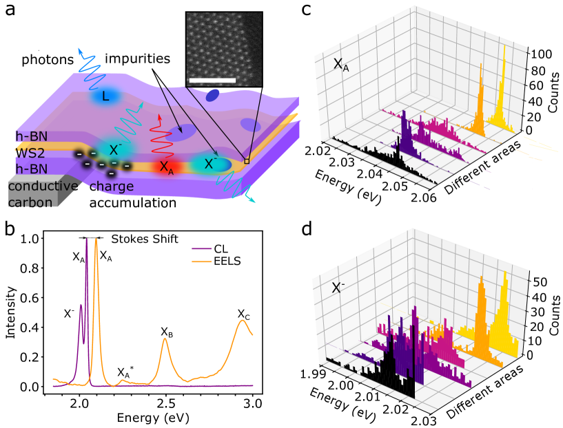
Here, we used transmission electron microscopy techniques including highly monochromated EELS, CL, high angle annular dark field (HAADF), and diffraction imaging to correlate sub-10 nanometer optical absorption and luminescence spectral mapping to structural and chemical mapping. We show that the trion and other localized (L) light emission energy and intensity can vary on scales down to tens of nanometers in WS2 monolayers while exciton emission intensity remains unchanged. In short, three effects are revealed: localized trion emission intensity increase at constant absorption rate due to either 1) chemical changes in tens of nanometer patches or 2) to charge accumulation in a metal-insulator-semiconductor heterostructure combined with near-field emission enhancement; and 3) the presence of a bright emission, attributed to L, below the trion energy, highly localized in space. These effects, sketched in Fig. 1a, are linked to local charge density variations and to near-field enhancement and not to the generally evoked local strain modification. In addition, the spatially-constant absorption, coupled to nanoscale-resolved CL, shows that the trion emission intensity increases due to a locally faster decay rate.
XA, X-, and the localized emission possibly linked to defects have been observed with CL in TMD monolayers before [18, 19, 20], utilizing specific sample heterostructures, but with only hundreds of nanometer spatial resolution. More importantly, previous reports of EELS measurements on TMD monolayers did not reach spectral resolution comparable with optical absorption experiments to allow for facile interpretation [21, 22, 23, 24]. An alternative technique, scanning tunnelling microscopy induced luminescence (STM-lum) allows the detection light emission from TMD monolayers [25, 26]. Despite the impressive atomic resolution achieved [26], the strong influence of the STM tip on optical spectra hinders their use as an nanoscale equivalent of PL.
The samples used here are made from WS2 monolayers exfoliated from bulk material, and encapsulated in h-BN (5 and 25 nm thick on each side). The heterostructures created are then deposited on a conductive carbon film (ten of nanometer thick) with 2 m-wide holes, itself supported on copper TEM grids (see the Methods section for details on sample preparation). The encapsulation offers high CL emission rate due to the increased interaction volume with the fast electron beam. The high charge-carriers density then produced enables CL detection [18, 19, 20]. High purity and homogeneity in the h-BN layers are critical to get spectral line shapes comparable to those using pure optical means. Four samples were analyzed, with a typical surface area of 150 .
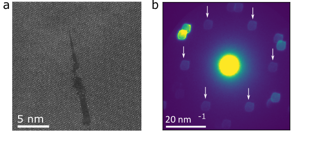
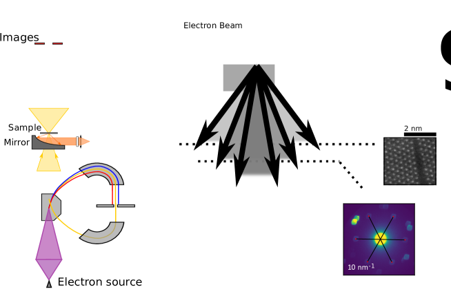
Experiments were performed in a scanning transmission electron microscope (STEM), in which spatially resolved data are acquired by scanning a subnanometer electron beam, retrieving images (2D arrays with an intensity value in each pixel) and datacubes (2D arrays with a spectrum or a diffraction pattern at each pixel), see Fig. SI3. Energy filtered maps can be produced by cuts of these datacubes at different energies. Structural information was retrieved from atomic scale images (Fig. 1a inset) and strain mapping through diffraction datacubes (Fig. SI2). For more information, see the Methods section.
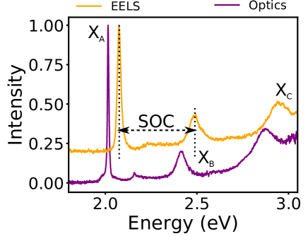
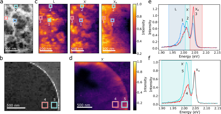
Fig. 1b presents the typical optical information that can be collected using CL and EELS on WS2 monolayers with the samples kept at 150 K. CL and EELS spectral resolution used were 8 and 26 meV, respectively, for the measurements presented here.
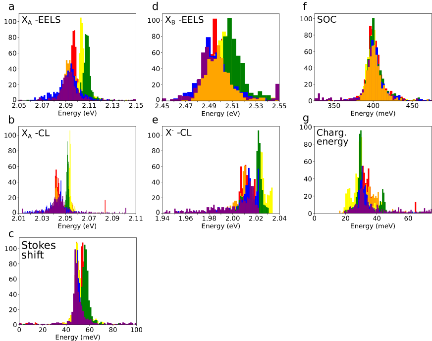
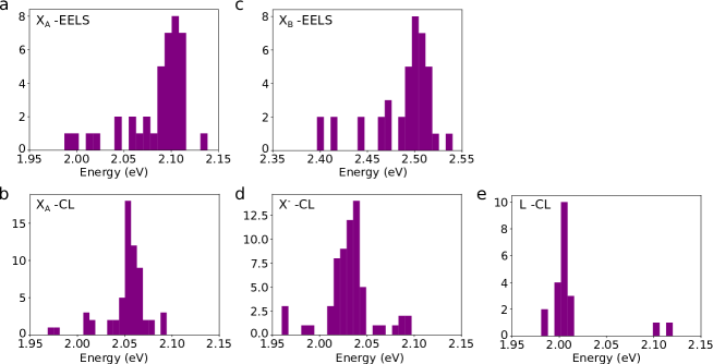
CL can be directly compared to off-resonance PL [27], where the emission from XA and X- (X+ occurs only in negatively gated WS2 [10]) is observed for the WS2 monolayer. An overview of the energies measured for XA and X- CL emission is plotted as histograms in Fig. 1c-d (more histograms corresponding to the localized L emission and exciton energies in EELS are shown in Fig. SI11), where the survey areas are of few m each (represented by a different color). The measurements average around 2.049 eV and 2.011 eV (with full width at half maxima (FWHM) 13 meV and 19 meV, respectively), showing agreement between ensemble of CL measurements across a sample with macroscopic optical measurements (typical variations are of 20 to 30 meV for XA emission and absportion in regions above 10 m2 [14, 8, 28, 29]). Regions with broader (15 meV, black histogram in Fig 1c-d) and narrower (5 meV, yellow histogram in the same figure) distributions can also be seen. In fact, of most interest in our study are the areas with spatial variations of the optical properties to unveil the origin of these variations.
For atomically thin materials, EELS measures the imaginary part of the dielectric function [30, 31], and it has been used for exciton mapping in TMDs [21, 22, 23, 24]. A comparison of the EELS and the optical absorbance (, where and are the optical reflectivity and transmission [8]) spectra of h-BN encapsulated WS2 at 150 K shows a one-to-one match between features (see Fig. SI1 and the Methods section for a discussion on EELS and optical absorption). The features seen in the EELS spectrum presented in Fig 1b are exciton peaks. In addition to XA and XB, two others are detected: X, the excited state of XA, and XC which arises from strong absorption due to band nesting around the point [32]. The energy positions of XA and XB measured in EELS are plotted as histograms in Fig. SI10 and Fig. SI11, showing the mean value of XA and XB to be 2.101 eV and 2.502 eV (with FWHM 24 meV and 25 meV, respectively).
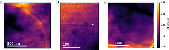
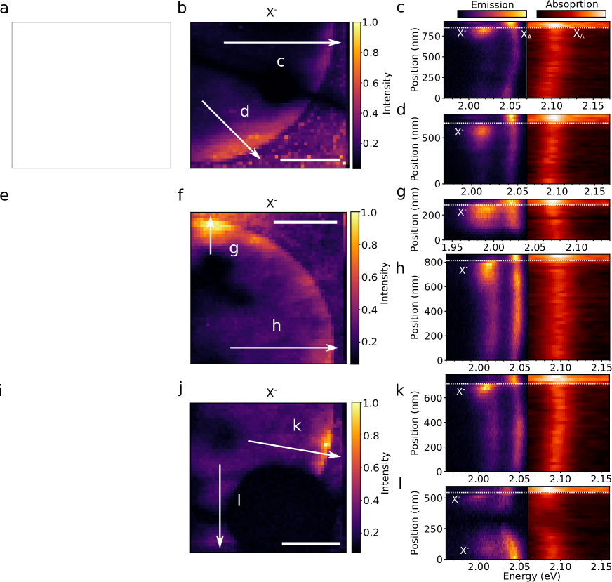
With this understanding of CL (EELS) as nanometer counterparts of PL (absorption), we can now describe our typical observations of deep sub-wavelength intensity variations, with examples shown in Fig. 2. X- and L peak intensities can vary locally in scales of tens of nanometers, while the XA peak intensity is relatively uniform. Fig. 2a and c show an example of this local intensity change for the X- and the L emission, which can occur for areas as small as 30x30 nm2. Spectra averaged in such small regions (Fig. 2e) show varying peak heights. This behavior is not homogeneous across a single h-BN/WS2/h-BN heterostructure or between different samples, and has been observed in regions of a few hundred nanometers across. A similar increase in X- intensity is observed close to edges of the carbon support (which appear as brighter regions in HAADF images, as in the upper right of Fig. 2b), which is in direct contact with the thicker (20 nm) h-BN layer (the sample details are described in the Methods section), but not with the WS2 layer. Indeed, filtered emission maps at the trion energy (Fig. 2d) have stronger intensities close to the edge, as observed systematically in other holes of the same heterostructure (see Fig. SI6) and of different samples. Spectra close to the edge (cyan curve in Fig. 2f) show stronger trion emission in comparison to those in the suspended region (red curve in Fig. 2f). At first glance, these emission modifications could have the same origin. Yet, they occur at different scales Figs. 3 (tens of nanometers) and 4 (above a hundred nanometers) further entailing a detail analysis.
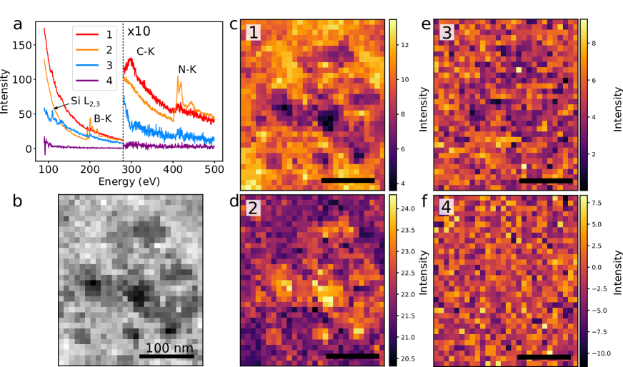
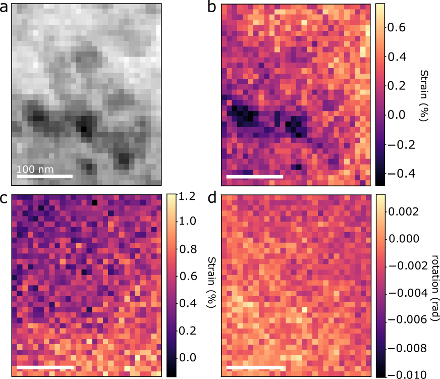
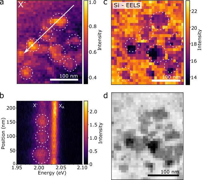
In suspended regions where the X- intensity varies locally while XA intensity remains constant (Fig. 3a-b and Fig. SI4), the typical spatial extension where enhanced trion emission is observed is of the order of tens of nanometers. As a function of position across different bright spots, the X- and XA intensities change independently (Fig. 3b), with no measurable energy shift. The typical size of these regions brings to mind the possibility of discrete light emitters, such as individual point defects, as observed in h-BN in the past [33] using CL. The trion formation and decay probabilities are known to depend on the local density of available free carriers, which can be modified not only by the presence of defects, but also by the local dielectric environment. HAADF images (Fig. 3d) of these regions show intensity variations, indicating the presence of extra matter either on the heterostructures’ interfaces or surfaces. Core loss EELS shows that in addition to the expected chemical species (S, B, and, N), traces of impurities including Si, C, and O are also detected. Silicon, carbon, and oxygen impurities are expected residues from the sample preparation during the exfoliation of layers.
Blind source separation spectral analysis (see Methods, and Fig. SI5) shows that a component with Si, C, and O content is anti-correlated to the appearance of localized X- emission maxima: a map of this component is shown in Fig. 3c. The localized trion emission occurs in the areas which lack this residue-related component (marked by dash circles in Fig. 3). These same patches appear as minima in an HAADF image (Fig. 3d, which is proportional to the projected atomic number; see Fig. SI5b, Fig. 2a-b, and the Methods section). Their presence do not prevent the excitation transfer from the h-BN to the monolayer, indicating they are thin (as also suggested by EELS). h-BN/TMD stacks can be very clean [34], but they contain some thin interface residue and bubbles. These additional surrounding dielectric patches change the local electromagnetic environment of the WS2 monolayer.
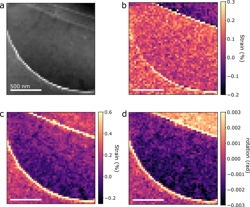
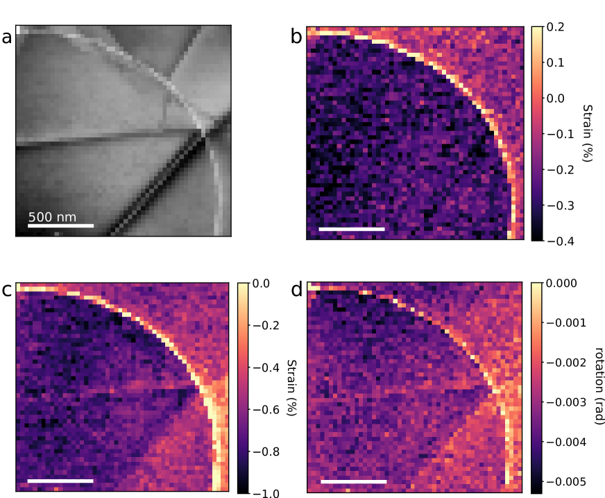
Around holes in the carbon support of the sample, the X- to XA ratio also increases (Fig. 4a-b and Methods). On top of the carbon support the XA emission increases, with a drastic decrease of the X- to XA ratio. A series of emission spectra acquired starting from the suspended region up to the hole’s edge along three different line profiles show the continuous increase in X- and XA emission. This evolution in emission occurs without observable modification of the absorption spectra (Fig. 4c-e, right panels). The same behavior occurs in most of the analyzed holes in the carbon support (three other examples are shown in Fig. SI6). A correlation between strain (Fig. 4a shows the component) and these modifications has not been detected (the bright lines occur due to structural changes including a fold and the carbon support edge).
In addition to the X- intensity increase, its peak emission energy varies towards the edge of the support (white curved arrow in Fig. 4d and Fig. SI6): initially the peak redshifts by about 20 meV over a distance of 200 nm, and as its intensity increases, the redshift is followed by a final abrupt shift back to its initial energy, over a distance of 50 nm, and a larger intensity increase. The energy shifts lead to broader emission X- histograms compared the XA (orange curves in Fig. 1c-d). Where this effect is observed, the XA emission and absorption energy do not follow the variations observed for the X-. However, along with this characteristic shift of the trion, other energy shifts are observed, which the XA does follow (Fig. 4c and Fig. SI6). These will be disentangled in the discussion.
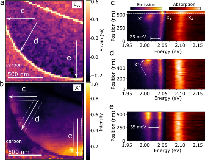
Finally, close to the carbon support edge, one also observes localized emissions which match the lower-energy transitions referred to as L in literature [14, 15, 8, 10] (Fig. 4, vertical profiles e in Fig. 4a-b). This emission can be separated from that of the trion since their energy splittings to the XA are different: XA - X- is 35 meV on average while XA - L is 45 meV. This particular energy splitting is systematically observed for this localized emission on the edge of the carbon support (observed on 21 measurements of 14 local emitters from two different samples). Its intensity is usually brighter than that of the trion, with an intensity ratio of = 3.4 on average, while it is of 1.3 for . The width of the L emission is about the same as that of the X-, respectively 31 and 33 meV, but larger than that of the XA is 17 meV, on average. The appearance of L emission could not be directly linked to patterns in strain maps.
The ensemble of observations concerning the trion can be explained by making a hypothesis based on local changes of the free electron density and of the dielectric environment. Trion emission intensity can be controlled by gating of III-V [35] and TMD [9] semiconductors, which controls the density of free electrons; conversely, chemical doping can also modify this quantity [36]. Unintentional doping in MoS2 has been shown to increase trion emission [37], while a similar increase in WS2 has been attributed to a larger concentration of defects [38]. Substrate modification has also demonstrated an effect on the trion emission intensity in WS2 monolayers [39]. In view of these reported observations, we attribute the localized trion emission increase described in Fig. 3 to an augmentation of the local free electron density due to the absence of the surface contaminants. It has also been observed that strain (0.6 and above) applied to WS2 monolayers [40] could induce trion intensity modification. Strain maps of regions around holes in the support do not show a correlation to the trion increase pattern (Fig. SI7). Our strain measurements are not precise below 1 for the buried WS2 monolayer (see Methods), so small deformations cannot be excluded. Finally, XA emission energy is not modified by the local dielectric patches. It is known that the optical bandgap of TMD monolayers is weakly influenced by the dielectric environment [16], as both the single particle bandgap and the exciton binding energy shift in tandem (to first order).
At first sight, one could invoke a similar interpretation to the increase in the X-/XA emission ratio close to the carbon support edge, that is, an effect of the local dielectric environment of the monolayer. However, given the sample geometry, the carbon support is not in contact with the monolayer, but separated by 20 nm of h-BN (the lower layer in the heterostructure), a thickness far larger than the extent of the exciton wavefunction outside the monolayer [7]. More importantly, the amorphous carbon of the TEM grids is conductive, which is one of the reasons for their routine use in TEM, and it would quench light emission from the monolayers (TMD monolayer deposited directly on TEM grids do not emit light in CL experiments).
It is exactly this conductive character of the carbon support that enters into play here. Our hypothesis is that the carbon support, h-BN, and WS2 heterostructure forms a metal-insulator-semiconductor (MIS) capacitor, as the WS2 is in contact with the carbon support away from measurement area. Therefore, free carriers at the center of the suspended region (distant from the carbon support) have different potential profiles than those in proximity to the carbon support. This changes the free carrier density at the center of the hole and around its edges, resulting in the different X-/XA emission ratio. Rough estimates show that the capacitance created by a 20 nm h-BN (considering its bulk dielectric function), given the difference in workfunction between amorphous carbon and WS2, can induce charge densities of the order of 1x cm-2. A x cm-2 increase in the electron density in WS2 (achieved by a 40 V gate voltage) has demonstrated an increase of the X- absorption intensity and a redshift of about 20 meV [9]. This energy shift matches the magnitude of that observed in Fig. 4c. In short, we interpret the redshift and higher emission rate as an increase in the trion population due to higher free electron concentration.
A second effect is observed, in addition to the redshift of the trion energy over 200 nm when approaching the carbon support; a blueshift of the trion which is in fact a shift back to its initial energy far from the carbon membrane. Along with this shift, an intensity increase at distances below 50 nm from the edge of the membrane is clearly visible. This is at first counterintuitive, as the former MIS capacitor explanation implies a continuous redshift with intensity increase. This second shift cannot be explained by a local change of the optical bandgap, since the energy of XA remains constant or changes marginally, both in absorption and emission (Fig. 4d) across the whole range. A simple reduction of the charge density would explain the shift back to initial energy, but not the increase in emission. We attribute this second shift and increase in intensity to a locally higher density of optical modes, which increases the decay rate due to the Purcell effect, where both the X- and XA are modified. A substantial increase in the emission intensity of molecules has been known to occur in close proximity to metallic structures [41].
In fact, such enhancement induces shorter exciton and trion lifetimes, leading directly to higher emission rates. It also explains the shift back in energy, which is related to the subsequent decrease of the trion population. We note that this is followed by an increase of XA emission, which is stronger on top of the carbon support (Fig. 4c, above the white dashed line), where the trion emission is reduced (Fig. 4d and SI6). We interpret this as a consequence of the reduction of the XA lifetime, which increases its emission rate and decreases the trion formation probability. Here, we note that absorption intensity does not increase, ruling out a larger emission intensity simply due to a larger excitation rate. That is, at a constant excitation rate, the total number of exciton and trion formation is fixed, leading to a competition between their emission intensities.
More specifically, the hypothesis of a trion blueshift due to strain is excluded because strain would also blueshift the XA emission and absorption energies, since it would change the WS2 optical bandgap. Notably, in other regions XA emission and absorption are observed to change locally, as in the profiles in Fig. 4c and Fig. SI6. These energy shifts are followed by the X-, but they do not preclude the general behavior demonstrated in Fig. 4d. Strain mapping (Fig. SI8) along the profiles in the regions where the XA energy (and X-) varies does not allow one to attribute the energy profiles solely to strain. Shear and tensile strain and in-plane rotation are observed, but a one-to-one correspondence between these and the energy variations was not detected in Fig. SI8 and Fig. SI9.
Finally, we return to the L emission observation. Strain maps of the monolayer close to the carbon support edges show that it is strained (see Fig. SI9 and Fig. SI8). The strain pattern is not simply that of a suspended membrane covering a circular hole, as one might initially expect. Indeed, regions close to the support edges show they can be under compression, including those where trion emission is increased. We interpret this as a result of the strain created during the heterostructure transfer.
This complex strain profile brings to mind the multiple observations of single photon emitters in TMDs [3, 4, 5, 6], specifically WSe2, which are currently attributed to the formation of localized excitonic states due to confinement. Previous experiments in suspended layers [3] and layers deposited over nanopillars [4, 6] show that strained layers lead to the formation of these single photon source. We do not observe a one-to-one correspondence of the appearance of L emission and strain maps. These emitters can be distinguished from trions based on their energy (they appear as distinct peaks in the binding energy histograms in Fig. SI10) and have spatial localization below 100 nm, similarly to single photon emitters detected in h-BN using CL [33]. These and other localized emitters in TMDs warrant further exploration at the nanometer and atomic scales.
In addition to allowing us to validate some hypothesis concerning energy shifts, the absorption and emission profiles shown in Fig. 4 give a local measure of the Stokes shift, the energy difference between emission and absorption of the same transition (XA here). In molecular systems this energy difference occurs due to the interaction with phonons. In semiconductors, in addition to phonon interaction, other phenomena can intervene, such as doping, strain, and substrate-related effects. The Stokes shift measured for our samples is of the order of 40 meV. This is much larger than the smallest reported values for bare or h-BN encapsulated WS2 monolayer [8, 29]. We attribute this difference to sample quality (source of WS2 or the heterostructure preparation), which further motivates future EELS and optical absorption experiments on the same objects.
The results presented here demonstrate the existence of nanometer scale localized light emission in relatively structurally homogeneous TMD monolayers, which can be attributed to variations of the free electron density in the material caused by surface residue modifying the dielectric environment locally. Trion mapping on TMDs could also be used as local dielectric sensor, similar to the suggestion by Xu et. al [16] based on optical reflectivity. From another perspective, the creation of nanoscale emitters indicate that dense arrays could be engineered by manipulation of the surface, such as by way of patterning. Finally, a lack of correlation between L emitters and strain above 1 indicates that strain alone is not sufficient for their generation. Possibly, point defects are necessary to generate them, as suggested by the detection of single photon emitters in h-BN encapsulated WSe2 placed on dielectric pillars only after 100 keV electron-irradiation [6]. As such, nanoscale electron microscopy and spectroscopy can offer a way to generate and characterize atomic-scale defects, and to monitor the change in optical response in real-time towards better understanding of nanoscale emitters in TMDs.
References
- Mak et al. [2010] K. F. Mak, C. Lee, J. Hone, J. Shan, and T. F. Heinz, Atomically thin MoS2: A new direct-gap semiconductor, Phys. Rev. Lett. 105, 136805 (2010).
- Xu et al. [2014] X. Xu, W. Yao, D. Xiao, and T. F. Heinz, Spin and pseudospins in layered transition metal dichalcogenides, Nat. Phys. 10, 343 (2014).
- Tonndorf et al. [2015] P. Tonndorf, R. Schmidt, R. Schneider, J. Kern, M. Buscema, G. A. Steele, A. Castellanos-Gomez, H. S. van der Zant, S. M. de Vasconcellos, and R. Bratschitsch, Single-photon emission from localized excitons in an atomically thin semiconductor, Optica 2, 347 (2015).
- Palacios-Berraquero et al. [2017] C. Palacios-Berraquero, D. M. Kara, A. R.-P. Montblanch, M. Barbone, P. Latawiec, D. Yoon, A. K. Ott, M. Loncar, A. C. Ferrari, and M. Atatüre, Large-scale quantum-emitter arrays in atomically thin semiconductors, Nature Comm. 8, 1 (2017).
- Darlington et al. [2020] T. P. Darlington, C. Carmesin, M. Florian, E. Yanev, O. Ajayi, J. Ardelean, D. A. Rhodes, A. Ghiotto, A. Krayev, K. Watanabe, et al., Imaging strain-localized exciton states in nanoscale bubbles in monolayer WSe2 at room temperature, Nat. Nano 15, 854 (2020).
- Parto et al. [2020] K. Parto, K. Banerjee, and G. Moody, Irradiation of nanostrained monolayer WSe2 for site-controlled single-photon emission up to 150 k (2020), arXiv:2009.07315 [physics.app-ph] .
- Molina-Sánchez et al. [2013] A. Molina-Sánchez, D. Sangalli, K. Hummer, A. Marini, and L. Wirtz, Effect of spin-orbit interaction on the optical spectra of single-layer, double-layer, and bulk MoS2, Phys. Rev. B 88, 045412 (2013).
- Arora et al. [2020] A. Arora, N. K. Wessling, T. Deilmann, T. Reichenauer, P. Steeger, P. Kossacki, M. Potemski, S. M. de Vasconcellos, M. Rohlfing, and R. Bratschitsch, Dark trions govern the temperature-dependent optical absorption and emission of doped atomically thin semiconductors, Phys. Rev. B 101, 241413 (2020).
- Chernikov et al. [2015] A. Chernikov, A. M. van der Zande, H. M. Hill, A. F. Rigosi, A. Velauthapillai, J. Hone, and T. F. Heinz, Electrical tuning of exciton binding energies in monolayer WS2, Phys. Rev. Lett. 115, 126802 (2015).
- Paur et al. [2019] M. Paur, A. J. Molina-Mendoza, R. Bratschitsch, K. Watanabe, T. Taniguchi, and T. Mueller, Electroluminescence from multi-particle exciton complexes in transition metal dichalcogenide semiconductors, Nat. Comm. 10, 1 (2019).
- Castellanos-Gomez et al. [2013] A. Castellanos-Gomez, R. Roldán, E. Cappelluti, M. Buscema, F. Guinea, H. S. van der Zant, and G. A. Steele, Local strain engineering in atomically thin MoS2, Nano Lett. 13, 5361 (2013).
- Schmidt et al. [2016] R. Schmidt, I. Niehues, R. Schneider, M. Drüppel, T. Deilmann, M. Rohlfing, S. M. De Vasconcellos, A. Castellanos-Gomez, and R. Bratschitsch, Reversible uniaxial strain tuning in atomically thin WSe2, 2D Materials 3, 021011 (2016).
- Frisenda et al. [2017] R. Frisenda, M. Drüppel, R. Schmidt, S. M. de Vasconcellos, D. P. de Lara, R. Bratschitsch, M. Rohlfing, and A. Castellanos-Gomez, Biaxial strain tuning of the optical properties of single-layer transition metal dichalcogenides, npj 2D Materials and Applications 1, 1 (2017).
- Jadczak et al. [2017] J. Jadczak, J. Kutrowska-Girzycka, P. Kapuściński, Y. Huang, A. Wójs, and z. Bryja, Probing of free and localized excitons and trions in atomically thin WSe2, WS2, MoSe2 and MoS2 in photoluminescence and reflectivity experiments, Nanotechnology 28, 395702 (2017).
- Koperski et al. [2017] M. Koperski, M. R. Molas, A. Arora, K. Nogajewski, A. O. Slobodeniuk, C. Faugeras, and M. Potemski, Optical properties of atomically thin transition metal dichalcogenides: observations and puzzles, Nanophotonics 6, 1289 (2017).
- Xu et al. [2021] Y. Xu, C. Horn, J. Zhu, Y. Tang, L. Ma, L. Li, S. Liu, K. Watanabe, T. Taniguchi, J. C. Hone, et al., Creation of moiré bands in a monolayer semiconductor by spatially periodic dielectric screening, Nat. Mat. , 1 (2021).
- Polman et al. [2019] A. Polman, M. Kociak, and F. J. G. de Abajo, Electron-beam spectroscopy for nanophotonics, Nat. Mat. 18, 1158 (2019).
- Zheng et al. [2017] S. Zheng, J.-K. So, F. Liu, Z. Liu, N. Zheludev, and H. J. Fan, Giant enhancement of cathodoluminescence of monolayer transitional metal dichalcogenides semiconductors, Nano Lett. 17, 6475 (2017).
- Nayak et al. [2019] G. Nayak, S. Lisi, W. Liu, T. Jakubczyk, P. Stepanov, F. Donatini, K. Watanabe, T. Taniguchi, A. Bid, J. Kasprzak, et al., Cathodoluminescence enhancement and quenching in type-i van der waals heterostructures: Cleanliness of the interfaces and defect creation, Phys. Rev. Materials 3, 114001 (2019).
- Singh et al. [2020] A. Singh, H. Y. Lee, and S. Gradečak, Direct optical-structure correlation in atomically thin dichalcogenides and heterostructures, Nano Res. 13, 1 (2020).
- Tizei et al. [2015] L. H. Tizei, Y.-C. Lin, M. Mukai, H. Sawada, A.-Y. Lu, L.-J. Li, K. Kimoto, and K. Suenaga, Exciton mapping at subwavelength scales in two-dimensional materials, Phys. Rev. Lett. 114, 107601 (2015).
- Habenicht et al. [2015] C. Habenicht, M. Knupfer, and B. Büchner, Investigation of the dispersion and the effective masses of excitons in bulk 2H-MoS2 using transition electron energy-loss spectroscopy, Phys. Rev. B 91, 245203 (2015).
- Nerl et al. [2017] H. C. Nerl, K. T. Winther, F. S. Hage, K. S. Thygesen, L. Houben, C. Backes, J. N. Coleman, Q. M. Ramasse, and V. Nicolosi, Probing the local nature of excitons and plasmons in few-layer MoS2, npj 2D Materials and Applications 1, 1 (2017).
- Hong et al. [2020] J. Hong, R. Senga, T. Pichler, and K. Suenaga, Probing exciton dispersions of freestanding monolayer WSe2 by momentum-resolved electron energy-loss spectroscopy, Phys. Rev. Lett. 124, 087401 (2020).
- Peña Román et al. [2020] R. J. Peña Román, Y. Auad, L. Grasso, F. Alvarez, I. D. Barcelos, and L. F. Zagonel, Tunneling-current-induced local excitonic luminescence in p-doped WSe2 monolayers, Nanoscale 12, 13460 (2020).
- Schuler et al. [2020] B. Schuler, K. A. Cochrane, C. Kastl, E. S. Barnard, E. Wong, N. J. Borys, A. M. Schwartzberg, D. F. Ogletree, F. J. G. de Abajo, and A. Weber-Bargioni, Electrically driven photon emission from individual atomic defects in monolayer WS2, Science Advances 6, 10.1126/sciadv.abb5988 (2020).
- Mahfoud et al. [2013] Z. Mahfoud, A. T. Dijksman, C. Javaux, P. Bassoul, A.-L. Baudrion, J. Plain, B. Dubertret, and M. Kociak, Cathodoluminescence in a scanning transmission electron microscope: A nanometer-scale counterpart of photoluminescence for the study of ii–vi quantum dots, J. of Phys. Chem. Lett. 4, 4090 (2013).
- Kolesnichenko et al. [2020] P. V. Kolesnichenko, Q. Zhang, T. Yun, C. Zheng, M. S. Fuhrer, and J. A. Davis, Disentangling the effects of doping, strain and disorder in monolayer WS2 by optical spectroscopy, 2D Materials 7, 025008 (2020).
- Niehues et al. [2020] I. Niehues, P. Marauhn, T. Deilmann, D. Wigger, R. Schmidt, A. Arora, S. M. de Vasconcellos, M. Rohlfing, and R. Bratschitsch, Strain tuning of the stokes shift in atomically thin semiconductors, Nanoscale 12, 20786 (2020).
- Hambach [2010] R. Hambach, Theory and ab-initio calculations of collective excitations in nanostructures: towards spatially-resolved EELS, Ph.D. thesis (2010).
- Kociak and Zagonel [2017] M. Kociak and L. Zagonel, Cathodoluminescence in the scanning transmission electron microscope, Ultramicroscopy 176, 112 (2017).
- Carvalho et al. [2013] A. Carvalho, R. Ribeiro, and A. C. Neto, Band nesting and the optical response of two-dimensional semiconducting transition metal dichalcogenides, Phys. Rev. B 88, 115205 (2013).
- Bourrellier et al. [2016] R. Bourrellier, S. Meuret, A. Tararan, O. Stéphan, M. Kociak, L. H. G. Tizei, and A. Zobelli, Bright UV single photon emission at point defects in h-BN, Nano Lett. 16, 4317 (2016).
- Haigh et al. [2012] S. Haigh, A. Gholinia, R. Jalil, S. Romani, L. Britnell, D. Elias, K. Novoselov, L. Ponomarenko, A. Geim, and R. Gorbachev, Cross-sectional imaging of individual layers and buried interfaces of graphene-based heterostructures and superlattices, Nature materials 11, 764 (2012).
- Teran et al. [2005] F. J. Teran, L. Eaves, L. Mansouri, H. Buhmann, D. K. Maude, M. Potemski, M. Henini, and G. Hill, Trion formation in narrow GaAs quantum well structures, Phys. Rev. B 71, 161309 (2005).
- Peimyoo et al. [2014] N. Peimyoo, W. Yang, J. Shang, X. Shen, Y. Wang, and T. Yu, Chemically driven tunable light emission of charged and neutral excitons in monolayer WS2, ACS Nano 8, 11320 (2014).
- Neumann et al. [2018] A. Neumann, J. Lindlau, M. Nutz, A. D. Mohite, H. Yamaguchi, and A. Högele, Signatures of defect-localized charged excitons in the photoluminescence of monolayer molybdenum disulfide, Phys. Rev. Materials 2, 124003 (2018).
- Lin et al. [2018] Y.-C. Lin, S. Li, H.-P. Komsa, L.-J. Chang, A. V. Krasheninnikov, G. Eda, and K. Suenaga, Revealing the atomic defects of WS2 governing its distinct optical emissions, Adv. Func. Mat. 28, 1704210 (2018).
- Kobayashi et al. [2015] Y. Kobayashi, S. Sasaki, S. Mori, H. Hibino, Z. Liu, K. Watanabe, T. Taniguchi, K. Suenaga, Y. Maniwa, and Y. Miyata, Growth and optical properties of high-quality monolayer WS2 on graphite, ACS Nano 9, 4056 (2015).
- Harats et al. [2020] M. G. Harats, J. N. Kirchhof, M. Qiao, K. Greben, and K. I. Bolotin, Dynamics and efficient conversion of excitons to trions in non-uniformly strained monolayer WS2, Nat. Photon. , 1 (2020).
- Anger et al. [2006] P. Anger, P. Bharadwaj, and L. Novotny, Enhancement and quenching of single-molecule fluorescence, Phys. Rev. Lett. 96, 113002 (2006).
- Tizei et al. [2020] L. H. Tizei, V. Mkhitaryan, H. Lourenço-Martins, L. Scarabelli, K. Watanabe, T. Taniguchi, M. Tencé, J.-D. Blazit, X. Li, A. Gloter, et al., Tailored nanoscale plasmon-enhanced vibrational electron spectroscopy, Nano Lett. 20, 2973 (2020).
- Krivanek et al. [2014] O. L. Krivanek, T. C. Lovejoy, N. Dellby, T. Aoki, R. W. Carpenter, P. Rez, E. Soignard, J. Zhu, P. E. Batson, M. J. Lagos, R. F. Egerton, and P. A. Crozier, Vibrational spectroscopy in the electron microscope, Nature 514, 209 (2014).
- Lagos et al. [2017] M. J. Lagos, A. Trügler, U. Hohenester, and P. E. Batson, Mapping vibrational surface and bulk modes in a single nanocube, Nature 543, 529 (2017).
- Qi et al. [2019] R. Qi, R. Wang, Y. Li, Y. Sun, S. Chen, B. Han, N. Li, Q. Zhang, X. Liu, D. Yu, et al., Probing far-infrared surface phonon polaritons in semiconductor nanostructures at nanoscale, Nano Lett. 19, 5070 (2019).
- Hachtel et al. [2019] J. A. Hachtel, J. Huang, I. Popovs, S. Jansone-Popova, J. K. Keum, J. Jakowski, T. C. Lovejoy, N. Dellby, O. L. Krivanek, and J. C. Idrobo, Identification of site-specific isotopic labels by vibrational spectroscopy in the electron microscope, Science 363, 525 (2019).
- Hage et al. [2020] F. Hage, G. Radtke, D. Kepaptsoglou, M. Lazzeri, and Q. Ramasse, Single-atom vibrational spectroscopy in the scanning transmission electron microscope, Science 367, 1124 (2020).
- Losquin et al. [2015] A. Losquin, L. F. Zagonel, V. Myroshnychenko, B. Rodríguez-González, M. Tencé, L. Scarabelli, J. Förstner, L. M. Liz-Marzán, F. J. G. de Abajo, O. Stéphan, and M. Kociak, Unveiling nanometer scale extinction and scattering phenomena through combined electron energy loss spectroscopy and cathodoluminescence measurements, Nano Lett. 15, 1229 (2015).
- Couillard et al. [2011] M. Couillard, G. Radtke, A. P. Knights, and G. A. Botton, Three-dimensional atomic structure of metastable nanoclusters in doped semiconductors, Phys. Rev. Lett. 107, 186104 (2011).
- Johnstone et al. [2020] D. N. Johnstone, P. Crout, M. Nord, J. Laulainen, S. Høgås, EirikOpheim, B. Martineau, T. Bergh, C. Francis, S. Smeets, E. Prestat, andrew ross1, S. Collins, I. Hjorth, Mohsen, T. Furnival, D. Jannis, E. Jacobsen, AndrewHerzing, T. Poon, H. W. Ånes, J. Morzy, phillipcrout, T. Doherty, affaniqbal, T. Ostasevicius, mvonlany, and R. Tovey, pyxem/pyxem: pyxem 0.12.3 (2020).
- de la Peña et al. [2020] F. de la Peña, E. Prestat, V. T. Fauske, P. Burdet, T. Furnival, P. Jokubauskas, M. Nord, T. Ostasevicius, K. E. MacArthur, D. N. Johnstone, M. Sarahan, J. Lähnemann, J. Taillon, pquinn dls, T. Aarholt, V. Migunov, A. Eljarrat, J. Caron, S. Mazzucco, B. Martineau, S. Somnath, T. Poon, M. Walls, T. Slater, actions user, N. Tappy, N. Cautaerts, F. Winkler, G. Donval, and J. C. Myers, hyperspy/hyperspy: Release v1.6.1 (2020).
- Pizzocchero et al. [2016] F. Pizzocchero, L. Gammelgaard, B. S. Jessen, J. M. Caridad, L. Wang, J. Hone, P. Bøggild, and T. J. Booth, The hot pick-up technique for batch assembly of van der waals heterostructures, Nature Com. 7, 1 (2016).
- Taniguchi and Watanabe [2007] T. Taniguchi and K. Watanabe, Synthesis of high-purity boron nitride single crystals under high pressure by using ba-bn solvent, Journal of Crystal Growth 303, 525 (2007).
- Stéphan et al. [2002] O. Stéphan, D. Taverna, M. Kociak, K. Suenaga, L. Henrard, and C. Colliex, Dielectric response of isolated carbon nanotubes investigated by spatially resolved electron energy-loss spectroscopy: From multiwalled to single-walled nanotubes, Phys. Rev. B 66, 155422 (2002).
.1 Acknowledgments
This project has been funded in part by the National Agency for Research under the program of future investment TEMPOS-CHROMATEM (reference no. ANR-10-EQPX-50) and from the European Union’s Horizon 2020 research and innovation programme under grant agreement No 823717 (ESTEEM3) and 101017720 (EBEAM). K.W. and T.T. acknowledge support from the Elemental Strategy Initiative conducted by the MEXT, Japan, Grant Number JPMXP0112101001, JSPS KAKENHI Grant Number JP20H00354 and the CREST(JPMJCR15F3), JST. This work has been supported by Region Île-de-France in the framework of DIM SIRTEQ”. We thank NION, HennyZ, and Attolight for the helpfull interaction on the adaptation of the CL system to the NION sample chamber on the ChromaTEM microscope and customization of the liquid nitrogen sample holder. We acknowledge the joint effort of the STEM team at the LPS-Orsay and, in particular Marcel Tencé and Xiaoyan Li, concerning instrumental developments. We thank Ashish Arora and co-authors for kindly providing the optical absorption data on a WS2 monolayer encapsulated in h-BN. Luiz F. Zagonel is acknowledged for ideas and discussion on data analysis.
.2 Competing interests
MK patented and licensed technologies at the basis of the Attolight Mönch used in this study, and is a part time consultant at Attolight. All other authors declare no competing financial interests.
I Supplementary information to Nanoscale modification of WS2 trion emission by its local electromagnetic environment
I.1 Methods
Scanning transmission electron microscopy (STEM) imaging, diffraction, CL and EELS experiments were performed on a modified Nion Hermes200 operated at 60 and 100 keV. In this microscope, subnanometer electron beams with sub 10 meV energy spread [42] can be generated for high spatial resolution imaging, diffraction and spectroscopy. High energy and spatial resolution have been substantially improved over the last ten years due to new monochromator technologies [43, 21, 44, 45, 46, 47]. The energy resolution of the EELS data presented here was between 20 and 30 meV (energy width of the primary electron beam). CL used a Mönch system from Attolight [31], with an energy resolution of 8 meV (minimum separation between two discernible emission peaks). Combined EELS-CL experiments have been used in the past to understand optical extinction and scattering in metallic plasmonic nanoparticles [48], but required much smaller requirements on the spectral resolution, due to the very large linewidth of the plasmons. Sample were kept at 150 K using a liquid nitrogen HennyZ sample holder for spectroscopic experiments, except for EELS chemical mapping. The typical exposure time used for CL and EELS low-loss experiment were 300 ms, and for core-loss and diffraction, 50 ms.
Atomically resolved imaging and spatially resolved EELS chemical maps were acquired on Nion UltraSTEM 200 operated at 100 keV, with the samples at room temperature. All images shown are high angle annular dark field (HAADF) images, in which the intensity is proportional to the projected atomic number, with W atoms showing as bright dots. The columns with two S atoms in projection are harder to pinpoint due to the background created by scattering in the h-BN layers. Diffraction effects play a smaller role in HAADF image intensity, so imaging with the h-BN slightly off-axis is beneficial to observe the single WS2 monolayer embedded in 25 nm of h-BN, as demonstrated before for CeSi clusters in Si matrices [49]. Encapsulation has also ensured a high stability of the monolayers under 60 keV and 100 keV electron irradiation, allowing imaging of free edges (Fig. 1a and Fig. SI2).
Diffraction patterns were acquired for each beam position on the sample with typical convergence semi-angle between 3 and 5 mrad and the camera dwell time was 50 ms. Diffraction mapping analysis was done with the Pyxem [50] and Hyperspy [51] python libraries. The quantity calculated is the displacement gradient tensor, corresponding to the difference between the deformed vectors and a reference, where the reference is a calculated vector with the reciprocal space length and orientation for unstrained WS2. A right-handed polar decomposition was used to separate deformation and rotation. The angle of rotation was then recovered from the rotation matrix. Each deformed vector was defined with the barycenter of the diffraction spots, and the center of the direct beam was first aligned with a cross correlation method. The barycenter method is limited by illumination changes of the diffraction spots (due to diffraction on the thicker h-BN layers), limiting our current strain measurements to above 1.
The CL and EELS datacube spectral fitting was done with the Hyperspy bounded multifit tool, using gaussian profiles. The Lorentzian profile was also tried since the EELS exciton peak profiles should be close to lorentzian, but the results are not displayed here to keep coherence for all curve fits. Most of the values found in the text are from mean spectra extracted from different regions of interest in each spectrum-image (these extracted spectra have a much higher signal to noise ratio). The extracted spectra are fitted with gaussian profiles, and the uncertainty associated is the standard deviation of the fit.
I.1.1 BSS+PCA analysis description
The blind source separation (BSS) technique consists of the separation of a mixed signal into individual components. The algorithm used in this paper was the independent component analysis (ICA) implemented in Hyperspy. In the ICA algorithm, the individual components are additive, and treated as non-gaussian and statistically independent. We chose 3 components, the first one contains the background, the h-BN and the carbon that are correlated together. This carbon can be from contamination of the sample. The second one contains the silicon and some carbon, and the third one contains mostly noise.
I.1.2 Sample preparation for electron spectroscopy and microscopy
h-BN/WS2/h-BN heterostructures were fabricated by using modified dry transfer method [52] then transferred to a TEM grid. WS2 was purchased from 2DSemiconductors and high quality h-BN synthesized by high pressure-high temperature method [53] was used. All constituted layers were first exfoliated onto a SiO2/Si substrate using the scotch-tape method [1]. A PDMS (polydimethylsiloxane) mask spin-coated by 15 PPC (polypropylene carbonate) is used for polymer stamp. PDMS is made by using the 20:1 ratio of Sylgard 184 pro-polymer to curing agent and kept at ambient conditions for overnight. To enhance adhesion between PDMS and PPC, PDMS mask was treated by oxygen plasma (18 W) for 5 min, before the spin-coating of PPC at 3000 rpm followed by heat treatment at 160 ∘C for 10 minutes. This polymer stamp was mounted to the micromanipulator upside down. A brief description of the procedures are described below.
-
1.
Pick-up exfoliated h-BN crystal from SiO2/Si substrate by contacting polymer stamp to the target crystal at 50 ∘C for 1 minute and lifting the stamp.
-
2.
Repeat step 1 to pick-up the monolayer WS2 crystal and bottom h-BN layer subsequently.
-
3.
Drop-down the stack (h-BN/WS2/h-BN) on a new SiO2/Si substrate by contact at higher temperature (120 ∘C) for 10 minutes.
-
4.
Clean the PPC residue on the surface with acetone and IPA.
-
5.
Anneal the heterostructure to enhance the interlayer coupling between constituent layers at 250 120 ∘C) for 6 hours in Ar environment.
-
6.
Spin-coat with polymethylmethacrylate (PMMA, 495K, Microchem) over the heterostructure at 3000 rpm followed by a heat treatment at 180 ∘C for 5 minutes.
-
7.
Etch SiO2/Si substrate by immerse the sample into KOH solution (1M) overnight.
-
8.
Transfer the sample to TEM grid (C-flat holey carbon grid with 2 m hole diameter)
-
9.
Remove PMMA residue by cleaning with acetone and IPA.
I.2 EELS and optical absorption comparison
The electromagnetic response properties of materials are usually described by its dielectric function . However optical measurements, usually give access to the complex refractive index, . These two quantities are linked by the relation , which also links their real and imaginary parts by
| (1) |
is the extinction coefficient, which is linked absorption coefficient, , by
| (2) |
with the wavelength of light. These two quantities, and , are linked to the decrease of the total intensity being transmitted through a medium.
A large part of optical absorption measurements are made from reflectivity, which gives access to reflectance, R:
| (3) |
from which and can be calculated using the Kramers-Kronig relation and a model taking into account the different dielectric layers in the sample under study.
Complications arise from the model necessary to extract the complex dielectric function, which can lead to modifications of line shapes. Therefore, measurements of an absorbance spectrum can be made, from which line shapes can be directly compared. However, this quantity is not a direct measure of any of the materials macroscopic constants. Of course, these can be extracted from the data.
EELS from an object with dielectric function measures . Therefore, in general, Kramers-Kronig transformation is required to retrieve and . However, for atomically thin objects it can be proven that is true. In this case, a direct comparison of measured by EELS for atomically thin layers and the calculated value from optical reflectivity is justified. Being a direct measure of , one can compare the line shapes of EELS with those in optical absorbance spectra (Fig. SI1). However, a comparison of exact energy positions requires one to take into account the dispersion of the real part of the dielectric function.
As discussed in the text, the energy shifts observed can be due to sample heterogeneity (Fig. SI11 show that the EELS spectra shift by at least 20 meV within our samples). But part of it can also come from the dispersion of . Nevertheless, we do not exclude fine differences between the quantities measured in EELS and optical absorption, in the tens of meV range. The fact that EELS for atomically thin structures measures has only been demonstrated at higher energies, with poorer energy precision (at 15 eV with 300 meV precision for single wall carbon nanotubes [54]).
I.3 Supplemental figures