Electroabsorption in gated GaAs nanophotonic waveguides
Abstract
We report on the analysis of electroabsorption in thin GaAs/Al0.3Ga0.7As nanophotonic waveguides with an embedded -- junction. By measuring the transmission through waveguides of different lengths, we derive the propagation loss as a function of electric field, wavelength, and temperature. The results are in good agreement with the Franz-Keldysh model of electroabsorption extending over 200 meV below the GaAs bandgap, i.e. in the 910–970 nm wavelength range. We find a pronounced residual absorption in forward bias, which we attribute to Fermi-level pinning at the waveguide surface, producing over 20 dB/mm loss at room temperature. These results are essential for understanding the origin of loss in nanophotonic devices operating in the emission range of self-assembled InAs semiconductor quantum dots, towards the realization of scalable quantum photonic integrated circuits.
An ambitious goal in photonic quantum technologies is to scale up photonic integrated circuits for generating, routing, and detecting single photons efficiently O’Brien, Furusawa, and Vučković (2009). One of the fundamental challenges is to keep the overall device and circuit loss as low as possible, as the fundamental no-cloning theorem of quantum mechanics forbids amplification of the single-photon signal. Gallium arsenide (GaAs) membranes with embedded self-assembled quantum dots (QDs) constitute a mature platform for integrating deterministic single-photon emitters with planar photonic integrated circuitsHepp et al. (2019); Lodahl (2017), with excellent single-photon source performance. Uppu et al. (2020a, b) Furthermore, the integration of doped layers in the epitaxial heterostructure, enables building thin -- diode junctions to control the state and charge occupation of the QD to reduce electrical noiseWang et al. (2016); Pedersen et al. (2020); Ollivier et al. (2020) and to tune the emitter wavelength via the quantum-confined Stark effect.Laucht et al. (2009) At the same time, however, the doped layers introduce additional loss due to free-carrier absorption and the Franz-Keldysh effect (FKE).Rosencher and Vinter (2002) The latter originates from the strong built-in electric fields in such thin junctions, which distort the electron and hole wave-functions in GaAs and enable optical absorption at energies below the bandgap.
In this work, we report on a detailed analysis of the various attenuation mechanisms in doped GaAs waveguides. We analyze the impact of electroabsorption and surface states on the waveguide loss. From the observed results, we conclude that a significant contribution to electroabsorption originates from strong band-bending at the surface of the waveguide, which is caused by mid-gap surface states. Previous works suggested that loss in doped waveguides can arise from unpassivated surfaces,Najer et al. (2019); Midolo et al. (2017) but no quantitative analysis has been reported. By comparing measurements with and without doped layers and at different temperatures, we can identify the origin of loss and devise a strategy for designing and fabricating the next generation of quantum photonic integrated devices with quantum emitters.
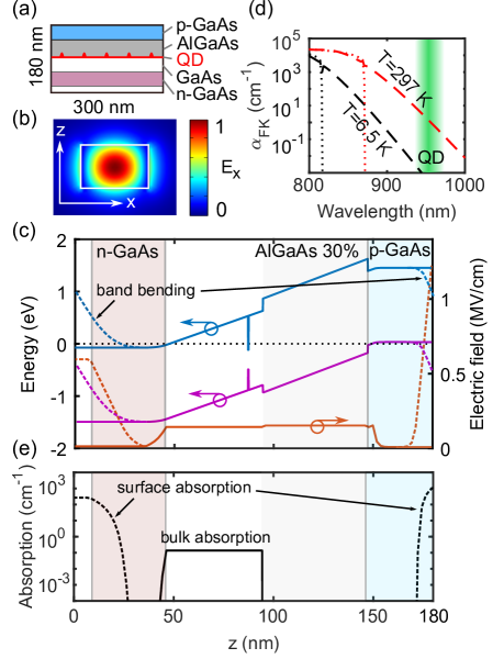
The devices used in this work are single-mode rectangular waveguides fabricated on a 180-nm-thick GaAs/Al0.3Ga0.7As membrane with a width of 300 nm. The layout of the structure and the profile of the fundamental transverse electric (TE) mode, , are shown in Fig. 1(a) and 1(b), respectively. The heterostructure contains a -- diode with a 100-nm-thick undoped region, with a layer of self-assembled InAs QDs located in the middle. The Al0.3Ga0.7As layer above the QDs serves as barrier to reduce the tunneling rate of holes out of the QDs, thereby extending the Stark tuning range of the emitter. Bennett et al. (2010) Further details on the heterostructure used in this work are given in ref.Uppu et al. (2020a). Figure 1(c) shows the diode band diagram at K, calculated with a one-dimensional Poisson equation solver, Tan et al. (1990) when no external voltage is applied to the diode. The solid lines show the conduction and valence band in the case of perfect ohmic contacts to the -type and -type layers. In a more realistic scenario, the waveguide surfaces have been exposed to air and have oxidized, producing a large amount of defects whose energy level is located within the GaAs bandgap. These mid-gap states are populated causing a net increase of surface charge density. The presence of surface defects is known to “pin” the Fermi level inside the gap, causing band bending in the proximity of the surface.Colleoni, Miceli, and Pasquarello (2015) To model the effect of the Fermi-level pinning, we apply a Schottky-type boundary condition with a barrier height of eV on both sides of the diode. The Schottky barrier height is estimated assuming a density of surface states cm-2,Offsey et al. (1986) which pins the Fermi level eV above the valence band maximum, as reported in previous experiments.Spicer et al. (1979) The bending of conduction and valence bands is shown in Fig. 1(c) as dashed lines. The corresponding electric field (with and without band bending) is plotted in Fig. 1(c) (right axis). Fields exceeding 1 MV/cm appear at the top surface due to Fermi-level pinning. Such large fields are expected to contribute significantly to the absorption due to the FKE, even several hundreds of meV inside the gap, where excitonic states of QDs are located.
To model the Franz-Keldysh absorption as a function of wavelength and electric field , we use the theory by Callaway,Callaway (1964) with the phenomenological scaling factors reported in ref. Stillman et al. (1976). These models and experiments cover the wavelengths (910–970 nm) and the electric field ranges of our experiment, but have been only experimentally validated at room temperature and in bulk GaAs. We assume that a change of temperature only affects the bandgap of GaAs, shifting it from eV at room temperature to eV at K, resulting in a lower absorption at cryogenic conditions. The calculated absorption for the two temperatures used in this work, together with the inhomogeneous distribution of QD emission, is shown in Fig. 1(d). The dotted lines show the typical zero-field absorption of direct-gap undoped semiconductors, i.e. when no absorption is expected at energies below the bandgap. The dashed lines show instead the absorption when kV/cm, i.e. when the FKE becomes significant in the QD emission region. In the model, the absorption due to QDs themselves has been neglected since the QD density m-2 and their absorption cross-section are too small to be observed when compared to all other loss mechanisms. Moreover, the quantum-confined Stark effect from QDs can also be neglected in our analysis, as the emitters’ inhomogeneous broadening ( meV) is much larger than the expected Stark tuning (in the order of 1 meV/V).
From the electric field profile calculated in Fig. 1(c) and the FKE model , a profile of the electroabsorption as a function of the position in the waveguide can be derived and it is plotted in Fig. 1(e). Here, we only plot the absorption due to the built-in electric field ( V) and surface fields due to Fermi-level pinning, while we neglect the electroabsorption in the Al0.3Ga0.7As region, as the bandgap is further blue-shifted to 1.77 eV. We further separate the contribution to the total absorption in two spatially distinct regions: 1) the undoped region inside the -- junction, where the absorption depends on the externally-applied bias (solid line in Fig. 1(e)) and 2) the surface regions, where the absorption is only due to Fermi-level pinning and does not depend significantly on the external field (dashed lines). We model the total loss in the waveguide as
| (1) |
where is the residual absorption (i.e. without the voltage-dependent FKE) and is the mode confinement factorVisser et al. (1997) for the undoped GaAs region, given by the overlap integral
| (2) |
Here, and are the simulated two-dimensional profiles of the optical mode electric field (cf. Fig.1b) and of the average Poynting vector component in the propagation direction of the waveguide, respectively, while is the spatial distribution of the permittivity. The subscript b denotes the undoped (bulk) GaAs layer in the waveguide. The electric field in the undoped region is calculated using , where is the total length of the undoped and depletion layer and is the built-in voltage of the diode junction.
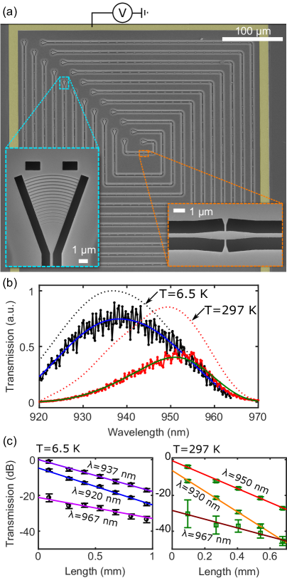
To measure the loss per unit length in nanophotonic waveguides, a series of concentric waveguides have been fabricated on the sample following the procedure outlined in a previous work.Midolo et al. (2015) The gratings are written with electron-beam lithography and etched via reactive ion etching in the same run, to ensure high reproducibility of their transmission spectrum within a 10% error. Figure 2(a) shows a top-view scanning-electron microscope (SEM) image of the fabricated sample. The p-contact electrode is highlighted in yellow and it is used to apply a voltage to the -- junction in the GaAs membranes. A pair of gratingsZhou et al. (2018) are used to couple light in and out of the waveguides. The gratings are placed at a fixed distance from each other, to avoid re-aligning the position and angle of excitation and collection beams, and cross-polarized to avoid collecting any scattered light from the input ports. This method allows factoring out the loss due to the gratings and the three 90-degree bends. Several tethers are used to keep the waveguide suspended in air, as shown in the inset of Fig. 2(a). Varying the number of tethers per unit length does not affect the transmission in our experiments,Papon et al. (2019) therefore we assume all tethers to be lossless. The sample is mounted in a closed-cycle cryostat and transmission measurements are performed using a supercontinuum laser source. Figure 2(b) shows the transmission spectra of the shortest waveguide m, at cryogenic and room temperature, without any bias applied to the diode. A visible quenching of the transmission is observed at room temperature, due to the built-in electroabsorption. Due to the thermo-optic effect, the grating transmission peak red-shifts by roughly 20 nm at room temperature. The small fringes, likely caused by the small reflectivity of the grating coupler, are smoothed out to extract a consistent response function at each wavelength (see solid lines in Fig. 2(b)). The fringe amplitude is used as an error bar for the transmission data. We note that the error bar typically exceeds the grating-to-grating variations due to fabrication and alignment errors. Figure 2(c) shows the transmission, in logarithmic scale, as a function of the waveguide length for both room and low temperatures. The attenuation coefficient is obtained by a linear fit of the logarithm of the transmission according to
| (3) |
where is the transmission of a single grating, derived from the intercept of the transmission curve with the ordinate, i.e. at zero length and is the transmission of a single 90-degree bend, which, from numerical simulations, accounts for m waveguide length and dB loss in the wavelength range investigated here. A loss per unit length of (17 1) dB/mm and (39 3) dB/mm is obtained at cryogenic and room temperature, respectively for the wavelengths of 937 nm and 950 nm, i.e. at the transmission peak of the gratings. Additionally, two fits are shown for wavelengths away from the central peak, where transmission is typically lower. Yet, the transmission in dB shows a linear dependence on the waveguide length within error bars, allowing us to extract a loss per unit length over a broader wavelength range. The grating transmission , obtained by the extrapolation described above, is shown as a function of wavelength in Fig. 2(b) as dotted lines. The grating transmission is compatible with results previously reported for undoped waveguides. Zhou et al. (2018) Also, the wavelength-dependence of the FKE is already visible by comparing the grating response and the measured data in Fig. 2(c): a more pronounced absorption is observed at shorter wavelengths than at longer wavelengths, as expected from theory (cf. Fig. 1(d)).
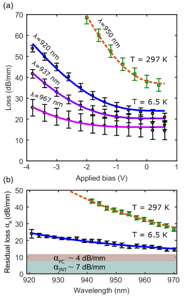
To identify the various contributions to loss in doped waveguides, the applied bias is varied from V (forward bias) to V (reverse bias) in steps of V and the measurement and fitting procedure described in Fig. 2 is repeated at all voltages. Figure 3(a) shows the dependence of the waveguide loss as a function of the applied bias for three different wavelengths at K and for the peak wavelength nm at room temperature. Error bars are given in logarithmic scale by propagation of uncertainties after fitting. A non-linear least-square fitting procedure is used to fit the data with the model of equation 1, where the fitting parameters are the confinement factor of the undoped region , and the residual loss. The residual loss is plotted in Fig. 3(b) as a function of wavelength and temperature. This is the loss which remains after compensating the built-in voltage in the waveguide. The pronounced wavelength-dependence of such residual loss suggests that an additional FKE is present, most likely due to the surface fields caused by Fermi-level pinning. We note that the loss per unit length extracted at wavelengths away from the grating peak would generally be more sensitive to variations between different samples. Nonetheless, all data analysis was carried out in a parameter range where such sample variations were minor compared to the extracted propagation loss.
To confirm this, the residual loss is fitted as a function of wavelength using the FKE model:
| (4) |
where we use a fixed field of MV/cm obtained from the simulated average surface field (cf. dashed line of Fig.1(c)). From the fit, the confinement factor of the surface region and the background loss are extracted. The solid lines show the best fit to the data. The results of the two fits of Fig. 3 are summarized in table 1, and compared to theoretical values obtained from finite-element calculations.
| K | K | Theory | |
| % | % | 52 % | |
| % | % | 4 % | |
| dB/mm | dB/mm | - | |
| dB/mm (estimated)Casey Jr, Sell, and Wecht (1975) | |||
| dB/mm (measured)Papon et al. (2019) | |||
Both low-temperature and room-temperature fits result in a constant background loss of dB/mm. Such loss can be attributed to sum of two main contributions, namely free-carrier absorption () and intrinsic loss (). Free-carrier absorption is estimated using the data for -doped and -doped layers given in ref Casey Jr, Sell, and Wecht (1975) and scaled by the confinement factors of equation 2, resulting in dB/mm. Intrinsic loss of waveguide is measured on a separate experiment that uses undoped wafers but identical waveguide geometry. The results have been previously published in ref.Papon et al. (2019) and resulted in dB/mm. The main source of intrinsic loss is suspected to be caused by scattering due to sidewall roughness arising in the GaAs etching process. The root-mean square (RMS) roughness in our waveguides is estimated to be in the – nm range from SEM analysis. According to waveguide scattering theory such as the Payne-Lacey model,Payne and Lacey (1994) roughness causes unwanted coupling between the fundamental guided mode and radiation modes, which is stronger for high-index contrast waveguides. A full three-dimensional finite-element simulation of transmission over rough waveguides provides a loss in the 5–8 dB/mm range, consistent with our experimental findings. Another potential loss mechanisms is given by the aforementioned mid-gap states which, even in the absence of doped layers, can cause absorption below the bandgap energy. However, further experiments are required to reduce the scattering loss and observe such loss mechanisms.
In conclusion, we have reported the analysis of electroabsorption in gated GaAs nanophotonic waveguides as a function of voltage, wavelength, and temperature. While the fundamental building blocks and devices for quantum applications can be realized over small ( m) dimensions, where the losses are negligible, scaling up photonic integrated circuits in doped GaAs requires a deep understanding of the origin of loss. To this end, it is crucial to devise a method to remove the sources of absorption while still operating at nm, i.e. the central wavelength of high-quality QDs. The -doped layer is the largest source of free-carrier absorption and it is only required on the emitter region. By selectively etching away the -layer from the surface, the free-carrier absorption can be reduced to dB/mm (i.e. the -layer contribution) and the FKE due to built-in fields can be suppressed. Surface fields, however, require strategies for unpinning the Fermi level. Several works have shown that oxide removal followed by surface passivation, greatly enhances the quality factor of microdisks, photonic crystal cavities and vertical microcavities.Guha et al. (2017); Najer et al. (2019); Kuruma et al. (2020) By removing mid-gap states, it is expected that the surface Fermi level unpins, thereby removing any source of electroabsorption due to band-bending. Finally, improving the fabrication process using intermediate hard masks González et al. (2014) or resist reflow Benevides et al. (2020) is also expected to reduce the waveguide RMS roughness to nm, which can potentially reduce the intrinsic waveguide loss down to dB/mm. Achieving such a target would enable integrating several hundreds of devices such as single-photon sources, filters, and switches, while taking advantage of the small size of such devices in the GaAs platform. For example, recently reported nanomechanical switches and filters,Papon et al. (2019); Zhou et al. (2020) have footprints of m, which would allow implementing large (-mode) unitary gates with mm optical depth, required for photonic quantum information processing.
Data availability statement
The data that support the findings of this study are available from the corresponding author upon reasonable request.
Acknowledgements.
We acknowledge Matthias Löbl, Alisa Javadi, and Richard J. Warburton for useful discussions. We gratefully acknowledge financial support from the Chinese Scholarship Council (CSC), Danmarks Grundforskningsfond (DNRF 139, Hy-Q Center for Hybrid Quantum Networks), H2020 European Research Council (ERC) (SCALE), Styrelsen for Forskning og Innovation (FI) (5072-00016B QUANTECH), Innovation Fund Denmark (9090-00031B, FIRE-Q), Bundesministerium für Bildung und Forschung (BMBF) (16KIS0867, Q.Link.X), Deutsche Forschungsgemeinschaft (DFG) (TRR 160).References
- O’Brien, Furusawa, and Vučković (2009) J. O’Brien, A. Furusawa, and J. Vučković, “Photonic quantum technologies,” Nature Photonics 3, 687–695 (2009).
- Hepp et al. (2019) S. Hepp, M. Jetter, S. L. Portalupi, and P. Michler, “Semiconductor quantum dots for integrated quantum photonics,” Advanced Quantum Technologies 2, 1900020 (2019).
- Lodahl (2017) P. Lodahl, “Quantum-dot based photonic quantum networks,” Quantum Science and Technology 3, 013001 (2017).
- Uppu et al. (2020a) R. Uppu, H. T. Eriksen, H. Thyrrestrup, A. D. Uğurlu, Y. Wang, S. Scholz, A. D. Wieck, A. Ludwig, M. C. Löbl, R. J. Warburton, et al., “On-chip deterministic operation of quantum dots in dual-mode waveguides for a plug-and-play single-photon source,” Nature Communications 11, 3782 (2020a).
- Uppu et al. (2020b) R. Uppu, F. T. Pedersen, Y. Wang, C. T. Olesen, C. Papon, X. Zhou, L. Midolo, S. Scholz, A. D. Wieck, A. Ludwig, and P. Lodhal, “Scalable integrated single-photon source,” Science Advances 6, eabc8268 (2020b).
- Wang et al. (2016) H. Wang, Z.-C. Duan, Y.-H. Li, S. Chen, J.-P. Li, Y.-M. He, M.-C. Chen, Y. He, X. Ding, C.-Z. Peng, C. Schneider, M. Kamp, S. Höfling, C.-Y. Lu, and J.-W. Pan, “Near-transform-limited single photons from an efficient solid-state quantum emitter,” Phys. Rev. Lett. 116, 213601 (2016).
- Pedersen et al. (2020) F. T. Pedersen, Y. Wang, C. T. Olesen, S. Scholz, A. D. Wieck, A. Ludwig, M. C. Löbl, R. J. Warburton, L. Midolo, R. Uppu, and P. Lodahl, “Near transform-limited quantum dot linewidths in a broadband photonic crystal waveguide,” ACS Photonics 7, 2343–2349 (2020).
- Ollivier et al. (2020) H. Ollivier, I. Maillette de Buy Wenniger, S. Thomas, S. C. Wein, A. Harouri, G. Coppola, P. Hilaire, C. Millet, A. Lemaître, I. Sagnes, O. Krebs, L. Lanco, J. C. Loredo, C. Antón, N. Somaschi, and P. Senellart, “Reproducibility of high-performance quantum dot single-photon sources,” ACS Photonics 7, 1050–1059 (2020).
- Laucht et al. (2009) A. Laucht, F. Hofbauer, N. Hauke, J. Angele, S. Stobbe, M. Kaniber, G. Böhm, P. Lodahl, M. Amann, and J. Finley, “Electrical control of spontaneous emission and strong coupling for a single quantum dot,” New Journal of Physics 11, 023034 (2009).
- Rosencher and Vinter (2002) E. Rosencher and B. Vinter, Optoelectronics (Cambridge University Press, 2002).
- Najer et al. (2019) D. Najer, I. Söllner, P. Sekatski, V. Dolique, M. C. Löbl, D. Riedel, R. Schott, S. Starosielec, S. R. Valentin, A. D. Wieck, et al., “A gated quantum dot strongly coupled to an optical microcavity,” Nature 575, 622–627 (2019).
- Midolo et al. (2017) L. Midolo, S. L. Hansen, W. Zhang, C. Papon, R. Schott, A. Ludwig, A. D. Wieck, P. Lodahl, and S. Stobbe, “Electro-optic routing of photons from a single quantum dot in photonic integrated circuits,” Optics Express 25, 33514–33526 (2017).
- Bennett et al. (2010) A. J. Bennett, R. B. Patel, J. Skiba-Szymanska, C. A. Nicoll, I. Farrer, D. A. Ritchie, and A. J. Shields, “Giant Stark effect in the emission of single semiconductor quantum dots,” Applied Physics Letters 97, 031104 (2010).
- Tan et al. (1990) I.-H. Tan, G. Snider, L. Chang, and E. Hu, “A self-consistent solution of Schrödinger–Poisson equations using a nonuniform mesh,” Journal of applied physics 68, 4071–4076 (1990).
- Colleoni, Miceli, and Pasquarello (2015) D. Colleoni, G. Miceli, and A. Pasquarello, “Fermi-level pinning through defects at GaAs/oxide interfaces: A density functional study,” Physical Review B 92, 125304 (2015).
- Offsey et al. (1986) S. Offsey, J. Woodall, A. Warren, P. Kirchner, T. Chappell, and G. Pettit, “Unpinned (100) GaAs surfaces in air using photochemistry,” Applied physics letters 48, 475–477 (1986).
- Spicer et al. (1979) W. Spicer, P. Chye, P. Skeath, C. Y. Su, and I. Lindau, “New and unified model for Schottky barrier and III–V insulator interface states formation,” Journal of Vacuum Science and Technology 16, 1422–1433 (1979).
- Callaway (1964) J. Callaway, “Optical absorption in an electric field,” Physical Review 134, A998 (1964).
- Stillman et al. (1976) G. Stillman, C. Wolfe, C. Bozler, and J. Rossi, “Electroabsorption in GaAs and its application to waveguide detectors and modulators,” Applied Physics Letters 28, 544–546 (1976).
- Visser et al. (1997) T. Visser, H. Blok, B. Demeulenaere, and D. Lenstra, “Confinement factors and gain in optical amplifiers,” IEEE Journal of Quantum Electronics 33, 1763–1766 (1997).
- Midolo et al. (2015) L. Midolo, T. Pregnolato, G. Kiršanskė, and S. Stobbe, “Soft-mask fabrication of gallium arsenide nanomembranes for integrated quantum photonics,” Nanotechnology 26, 484002 (2015).
- Zhou et al. (2018) X. Zhou, I. Kulkova, T. Lund-Hansen, S. L. Hansen, P. Lodahl, and L. Midolo, “High-efficiency shallow-etched grating on GaAs membranes for quantum photonic applications,” Applied Physics Letters 113, 251103 (2018).
- Papon et al. (2019) C. Papon, X. Zhou, H. Thyrrestrup, Z. Liu, S. Stobbe, R. Schott, A. D. Wieck, A. Ludwig, P. Lodahl, and L. Midolo, “Nanomechanical single-photon routing,” Optica 6, 524–530 (2019).
- Casey Jr, Sell, and Wecht (1975) H. Casey Jr, D. Sell, and K. Wecht, “Concentration dependence of the absorption coefficient for n- and p- type GaAs between 1.3 and 1.6 ev,” Journal of Applied Physics 46, 250–257 (1975).
- Payne and Lacey (1994) F. Payne and J. Lacey, “A theoretical analysis of scattering loss from planar optical waveguides,” Optical and Quantum Electronics 26, 977–986 (1994).
- Guha et al. (2017) B. Guha, F. Marsault, F. Cadiz, L. Morgenroth, V. Ulin, V. Berkovitz, A. Lemaître, C. Gomez, A. Amo, S. Combrié, et al., “Surface-enhanced gallium arsenide photonic resonator with quality factor of ,” Optica 4, 218–221 (2017).
- Kuruma et al. (2020) K. Kuruma, Y. Ota, M. Kakuda, S. Iwamoto, and Y. Arakawa, “Surface-passivated high-Q GaAs photonic crystal nanocavity with quantum dots,” APL Photonics 5, 046106 (2020).
- González et al. (2014) I. P. González, L. E. Munoz Camunez, A. G. Taboada, C. Robles Urdiales, J. M. Ripalda Cobian, and P. A. Postigo Resa, “Fabrication of high quality factor GaAs/InAsSb photonic crystal microcavities by inductively coupled plasma etching and fast wet etching,” Journal of Vacuum Science & Technology B 32, 011204 (2014).
- Benevides et al. (2020) R. Benevides, M. Ménard, G. S. Wiederhecker, and T. P. M. Alegre, “Ar/Cl2 etching of GaAs optomechanical microdisks fabricated with positive electroresist,” Optical Materials Express 10, 57–67 (2020).
- Zhou et al. (2020) X. Zhou, R. Uppu, Z. Liu, C. Papon, R. Schott, A. D. Wieck, A. Ludwig, P. Lodahl, and L. Midolo, “On-chip nanomechanical filtering of quantum-dot single-photon sources,” Laser & Photonics Reviews 14, 1900404 (2020).