Observing separate spin and charge Fermi seas in a strongly correlated one-dimensional conductor
An electron is usually considered to have only one form of kinetic energy, but could it have more, for its spin and charge, by exciting other electrons? In one dimension (1D), the physics of interacting electrons is captured well at low energies by the Tomonaga-Luttinger model, yet little has been observed experimentally beyond this linear regime. Here, we report on measurements of many-body modes in 1D gated-wires using tunnelling spectroscopy. We observe two parabolic dispersions, indicative of separate Fermi seas at high energies, associated with spin and charge excitations, together with the emergence of two additional 1D ‘replica’ modes that strengthen with decreasing wire length. The effective interaction strength is varied by changing the amount of 1D inter-subband screening by over 45%. Our findings demonstrate the existence of spin-charge separation in the whole energy band outside the low-energy limit of validity of the Tomonaga-Luttinger model, and also set a constraint on the validity of the newer nonlinear Tomonaga-Luttinger theory.
Introduction
Many-body systems cannot be explained by studying their individual components, with interactions often giving rise to collective excitations from which an array of qualitatively new quasi-particles starts to emerge. This is particularly striking in one dimension (1D), as here geometrical confinement alone imposes strong correlations in the presence of any interactions, leading to well-known non-Fermi-liquid phenomena such as spin-charge separation (?). Overall, the behaviour of 1D interacting gapless systems in the low-energy regime is well captured by the Tomonaga-Luttinger model (?, ?, ?), and has been extensively tested in carbon nanotubes (?, ?, ?), semiconductor quantum wires (?, ?, ?), antiferromagnets (?) and more recently, cold-atom chains (?). The model, which assumes a linearised single-particle dispersion, is expected to only be valid close to the Fermi points, where nonlinearities are still weak. However, pronounced consequences of band curvature have also very recently started to be explored experimentally (?, ?, ?).
At the same time, modelling such systems is a long-standing open problem. Simultaneous introduction of the charge and spin degrees of freedom into a nonlinear extension of Tomonaga-Luttinger-liquid (TLL) theory (?) predicted that the spin-charge separation would no longer exist beyond the low-energy regime (?, ?), since the holons (i.e., charge-type excitations) are made unstable by the nonlinearities. Instead, a mixture of spinons (i.e., spin-type excitations) and holons is responsible for the power-law threshold behaviour around the spectral edges. Extra, higher-order 1D modes, which have the spectral edge dispersion shifted and mirrored from that of the main 1D subband, were predicted in (?) as well. Another theory (?) showed that these extra modes should only emerge as the system length is reduced. We have observed some signatures of these ‘replicas’ in the past (?, ?), but experimental results beyond the linear regime that have both enough resolution and clarity to distinguish between predictions have been lacking.
Here, we measure the spectral function for the spin and charge excitations well beyond the linear regime using a tunnelling spectroscopy technique that allows mapping in both energy and momentum space. In the amplitude of our signal, we observe for the first time how the two branches of the linear TLL modes evolve away from the Fermi points into two fully formed nonlinear dispersions that consist of purely spin or charge collective modes, identified by comparison with the spectra predicted by the 1D Fermi-Hubbard model (?). Both dispersions are parabolic in shape but with different masses, implying the existence of two Fermi seas of different types. This result shows that the spin and charge collective excitations both remain stable in the whole conduction band, well beyond the low-energy limit of the original Tomonaga-Luttinger model where their existence was first established. We are able to tune the degree of screening of the Coulomb interaction by changing the confinement in our wires and so the number of occupied subbands. This is accompanied by a variation of approximately 45% of the two-body interaction energy and allows us to trace how both Fermi seas evolve as the interaction strength is varied. Measuring wires of different lengths, we are also able to observe two, with a possible third, separate 1D nonlinear ‘replica’ modes of the spinon type that systematically emerge as the length decreases.
Results
Characterisation of the 1D array
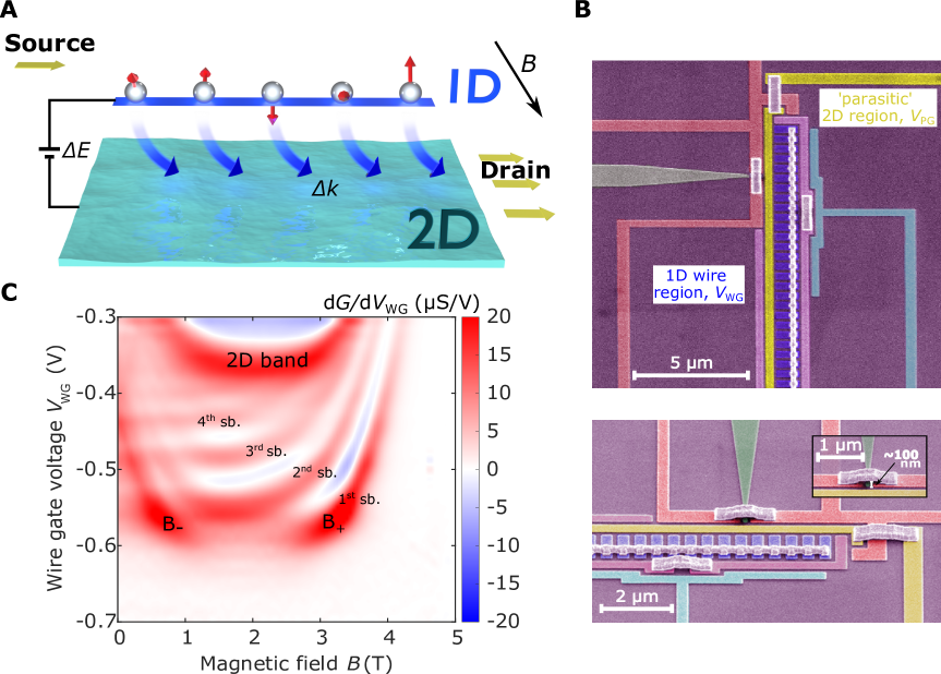
Our experiment consists of a tunnelling spectrometer made on a heterostructure with two parallel quantum wells (QWs), grown by molecular-beam epitaxy (MBE). We measure the tunnelling conductance between the 1D wires and the 2D layer at lattice temperatures mK (see Fig. 1A), where is the tunnelling current while the DC bias applied between the layers. Tunnelling occurs when filled states in one system have the same energy and momentum as empty states in the other, therefore ensuring that both energy and momentum are conserved. In order to map the dispersion of each system, a negative (positive) voltage applied to the 1D wires provides energy for tunnelling from (to) 1D states below (above) the Fermi level, while an in-plane magnetic field perpendicular to the wires boosts the momentum, offsetting the spectral functions of each system by , where is the electronic charge and the separation between the wells. The differential tunnelling conductance displays resonant peaks corresponding to maximal overlap of the offset spectral functions (dispersion relations). The device therefore behaves as a spectrometer, with the well-characterised 2D system being used to probe the less-well understood spectral function of the 1D system.
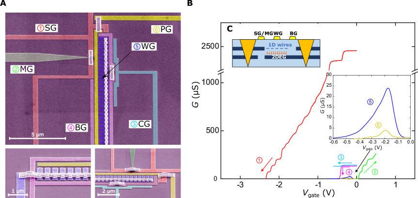
We use a surface-gate depletion technique in order to establish separate contacts to each well. Our 1D system consists of an array of 400 highly regular quantum wires formed in the upper layer by using a set of wire gates (WGs) fabricated on a Hall bar via standard electron-beam lithography and connected by air bridges (see Fig. 1B and inset) (?). Use of an array averages out impurities, length resonances and charging effects as well as increasing the overall strength of the measured signal. For the shorter devices, the air bridges are crucial for ensuring that good uniformity is obtained along the entire length of the wire, which would otherwise become narrower at one end if instead all the gates were joined by a continuous metal strip. Current is injected into the 1D wires via a small region, 0.45 m wide. Unlike the wires, however, this region is 2D in nature and its parasitic signal can be readily distinguished from the 1D signal in the measured data since its density is different. We use the unconfined weakly interacting 2D electron gas (2DEG) in the bottom well as a well-understood spectrometer. Note that our measurement is subject to capacitive effects between the wells, as well as between each well and the surface gates, and we take these into account in all the curves we plot, see Supplementary Text section 1.6.1.
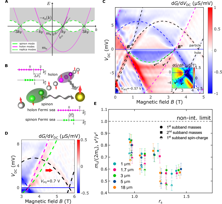
A plot of vs and shows U-shaped curves, one per 1D subband (Fig. 1C). We start our experiment by choosing so that there is just one 1D subband occupied. Fig. 2C shows an example of such a measurement, with conductance through the sample being measured as a function of energy () and momentum (). Here, the tunnelling map can be divided into two sectors, particle (for 0) and hole (for 0), corresponding, respectively, to electrons tunnelling into and out of the wires. The 1D Fermi wave vector is determined from the crossing points ( and ) along the line. The electron density in the wires is , which then gives the interaction parameter , where is the Bohr radius of conduction electrons in GaAs, see Supplementary Text section 1.5. The density can be controlled by tuning , reducing it down to m-1 before the wires pinch off.
Observation of two Fermi seas for spin and charge
The curves drawn over the data in Fig. 2C are those expected from single-electron tunnelling processes. Undesirable yet unavoidable ‘parasitic’ tunnelling coming from the narrow 2D injection region (marked by the dashed black curves, see Supplementary Text section 1.6.2) produces a background in the form of a set of parabolic dispersions, which can be subtracted once separately mapped (with the wire gates pinched off). On the other hand, dashed blue curves reveal the elementary excitations of the 2D lower well, as probed by the 1D wires. The remaining strong features, marked by the green and magenta dashed curves, arise from the 1D system. We are unable to explain these data well using a single parabola (see Supplementary Text section 1.6.3 for details), a fact that strongly points in the direction of separate spin and charge modes.
In order to identify whether this is the case, we interpret the 1D tunnelling signal using the dispersion of the 1D Fermi-Hubbard model in the semiconductor limit, in which many-body spectra are described completely by the Lieb-Wu equations (?). This system of nonlinear coupled equations is solved for two types of momentum states, (for charge) and (for spin degrees of freedom), which for the ground state form two filled Fermi seas marked by filled circles of two different colours in Fig. 2B (for a detailed discussion of the theoretical model, see sections 1.1, 1.2, and 1.3 of the Supplementary Text). An excitation, say an electron tunnelling out of the wire, removes one charge and one spin simultaneously to reassemble a free electron, marked by a pair of green and magenta empty circles in Fig. 2B. Placing the hole of one type at its corresponding Fermi energy and moving the other one through the band describes the spectrum of the purely holon or purely spinon modes. While the momentum of these collective excitations as a whole is well-defined due to the translational invariance, with or , the constituent degrees of freedom form non-equidistant distributions of their (quasi-)momenta, which depend in detail on the interaction strength and the positions of the two holes, owing to the strongly correlated nature of the model. Explicit solution of the Lieb-Wu equations for and for the two kinds of pure excitations produces the two dispersions drawn as the magenta and green solid lines in Fig. 2A. These two dispersions constructed out of collective modes for spin and charge have a shape close to parabolic, and have a simple description in terms of two Fermi seas with different masses. This closely matches our experimental observations, implying the presence of these two Fermi seas (see section 1.6 of the Supplementary Text) in a real system of interacting electrons.
Around the points, these curves are almost linear, and can be characterised by two different slopes and , parameters of the spinful Tomonaga-Luttinger model for the holon and spinon modes, respectively. These two velocities are related microscopically to the Hubbard interaction parameter (?, ?), and the spectral function predicted by the linear Tomonaga-Luttinger theory displays two strong peaks on these two branches (?, ?), which have already been measured in semiconductor quantum wires (?, ?). Away from the Fermi points, the spectra of holons and spinons extend naturally to the nonlinear region, evolving into two separate curves that are close to parabolae described by masses and , respectively. These shapes indicate formation of two separate Fermi seas by the nonlinear excitations. Their dispersions cross the Fermi energy at two different pairs of Fermi points ( and ), see a numerical simulation of the Fermi-Hubbard model via the dynamical density-matrix renormalization group method in (?), since the number of holons is twice the number of spinons for the spin-unpolarised wires in our experiments, making the densities for the two kinds also different by the same factor. The ratio of their masses depends on , deviating further from the free-particle value with increasing interaction strength.
As we have seen, the dispersion of the strongest features in the experimental 1D signal (marked by dashed green and magenta lines in Fig. 2C) cannot simply be interpreted using only a single parabola, corresponding to a single Fermi sea. This can be further established by analysing the tunnelling signal at zero field, see Supplementary Text section 1.6.4 for details. If, instead of just one parabola, we use two, corresponding to two Fermi seas, such as that predicted by the Fermi-Hubbard model, then we can match the experiments well. We observe two modes in our data, which match the dispersions of pure excitations of the two different kinds depicted in Fig. 2A, where two distinct Fermi seas are formed by the nonlinear spinon and holon collective modes out of the many-body continuum away from the Fermi points. This result demonstrates a non-perturbative effect that interactions cause in the whole band in 1D, posing a new theoretical challenge of accounting for higher-order processes beyond what has been considered in the literature so far (?) to describe it.
While we observe two dispersions in the hole sector, only one is visible in the particle sector, which we easily associate with the holon Fermi sea, as its gradient matches that of the charge line in the hole sector. At the same time, the spinon dispersion that assumes a naïve extension from the hole sector is systematically absent in the particle sector for all devices measured, see green dashed line in Fig. 2D. This result is, however, compatible with the particle-hole asymmetry in relaxation times of hot carriers as reported previously in (?). Even though spin and charge excitations were not resolved in (?), assuming that the spinon branch in the particle sector is unstable (so that we do not observe it), there would be an accelerated relaxation for hot electrons as they eventually split into spinon and holons. Note that the spinon Fermi sea alone has already been observed by neutron scattering (probing the dynamic structure factor instead of the spectral function that we measure here) in antiferromagnetic spin chains realised in insulating materials (?, ?, ?) as a spectral edge with a nonlinear dispersion separating the multi-spinon continuum from a forbidden region (?, ?). In these experiments the spectral power of the excitations drops very rapidly towards the particle part of the spinon dispersion making it therefore undetectable. Also note that, in the present experiment, the charges are delocalised as well, permitting us to see both Fermi seas at the same time.
By tuning the confinement in the wires we are also able to change the number of occupied subbands and their respective densities, therefore allowing us to follow the evolution of each Fermi sea as is changed by a significant amount. Such statistics collected from a range of samples in Fig. 2E show a systematic trend of larger deviations of the observed ratio from its non-interacting value with increasing . The ratio of the Luttinger parameters simultaneously extracted from the same data (see as an example the inset in Fig. 2C) exhibits a very similar dependence on .
Further interaction signatures: a hierarchy of 1D ‘replica’ modes
Having now identified two separate Fermi seas for spin and charge in our data, we further analyse the 1D dispersion by contrasting it with the simulated tunnelling conductance map between a non-interacting 1D system and a 2DEG (see Fig. 3A). Note how, unlike in Fig. 2C, it is possible to fit both particle and hole sectors of the map with a single parabola (dashed magenta). This is because, in the absence of interactions, the opposite spin states are degenerate, leaving room for only a single Fermi sea. We start by examining the region just above (i.e. +), where a clear feature not accounted for by our non-interacting simulation can be observed, see Fig. 3B. Here, the tunnelling conductance peak broadens and splits, with one boundary following the 1D holon mode while the other branches away from it. In order to isolate it from any potential background contamination, we apply a positive again in order to move the ‘parasitic’ resonance signatures away from . We also observe that this extra feature is not visible once the wires are past pinch-off, and that it is independent of the ‘parasitic’ tunnelling signal.
The mode-hierarchy picture for fermions (?, ?) predicts that the continuum of the many-body excitations separates itself into levels (i.e., first and higher orders) by their spectral strengths, which are proportional to integer powers of (i.e., this parameter to the first and higher powers), where is the length scale related to the interaction and is the length of the system (see Supplementary Text section 1.4 for more details). The principal (spin and charge) parabolae have then the largest amplitude, while their mirrors with respect to the chemical potential (i.e., ) and translations by integer multiples of manifest themselves as ‘replicas’, see dashed lines on Fig. 2A, with amplitudes proportional to higher powers of the small parameter . We have observed this feature in samples with wire lengths ranging from 1 m to 18 m, with all devices being mapped at very similar densities and Fermi energies, making them otherwise similar in . In all of them the strength of the mode marked by the dotted blue line in Fig. 3B, which is a ‘replica’ of the parabola formed by nonlinear spinons, decreases as the field is increased away from the crossing point. However, once the background has been subtracted and has been normalised by length, one can see qualitatively that the decay away from was slower the shorter the 1D system, as predicted, with the signal vanishing at higher momenta away from .
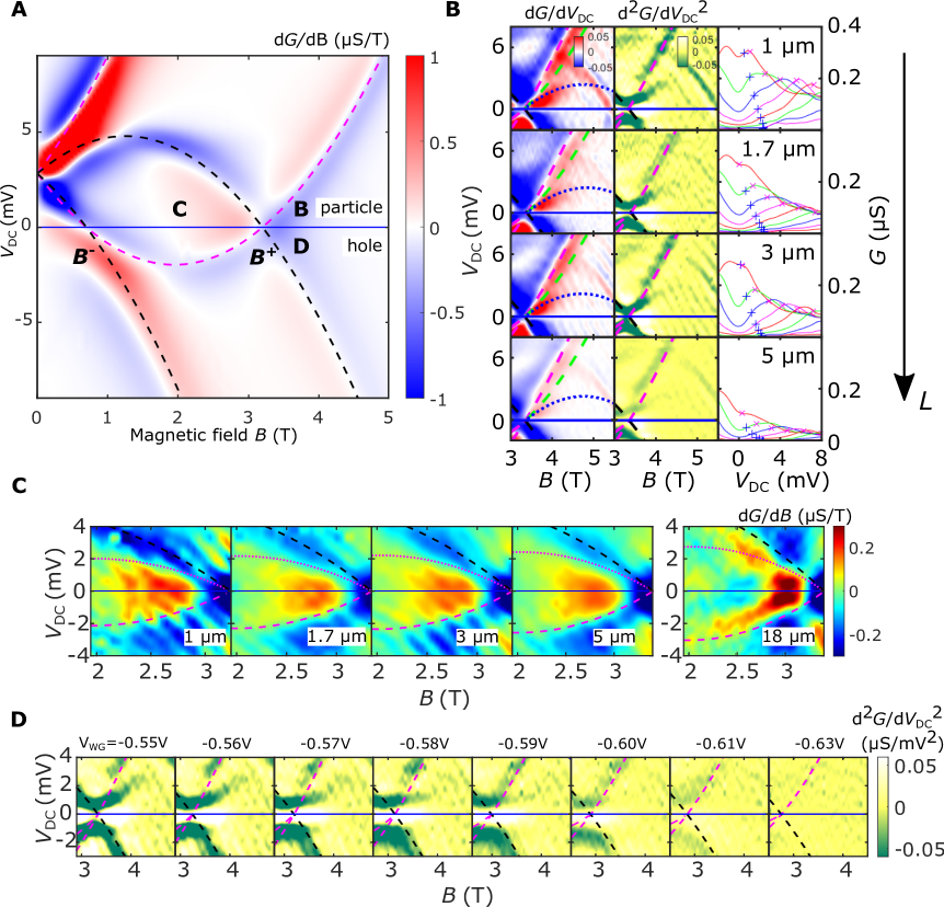
In order to test our prediction of length-dependent spin-type ‘replica’ modes further, we have looked at two other sectors of the tunnelling map, see Fig. 3C and D. We initially reported the first mode between as an inverted (spinon) shadow band symmetric to the 1D (spinon) mode in (?). According to the nonlinear theory of TLLs (?, ?), in the main region of the hole sector, the edge of support (defined as the hole excitation with the smallest possible energy for a given momentum) is predicted (?, ?) to coincide with the spinon mass shell, whose dispersion we have already observed to be very close to a parabola in our experiment. Similarly, in the main region of the particle sector, the edge of support is also predicted to be given by the inverted spinon mass shell in Fig. 2A. Consistent with the nonlinear theory, a symmetric inverted replica was seen in the particle sector, opposite to the main 1D subband, in all mapped devices, up to 5m (see Fig. 3C). This feature can also be seen in Fig. 2C. According to the mode-hierarchy picture, a length dependence similar to that of Fig. 3B is also expected to be observed since this is also a sub-leading mode. Although such dependence is not particularly clear from m, the replica mode was seen to not be present at all for the 18 m wire.
Similarly, another ‘replica’ mode is also predicted to exist at , symmetric to the sub-leading spinon mode shown in Fig. 3B, but in the hole sector. Only for the shortest, 1 m device is a feature consistent with this picture starting to be observed, hinting that a full observation of this mode would probably only happen at sub-micron lengths. Nevertheless, as seen in Fig. 3D, both modes evolve in tandem with each other as the 1D channels are squeezed towards pinch-off. This further establishes that these features are 1D in nature and cannot originate from the ‘parasitic’ injection region. All three replica features discussed emerge as the effective length of the 1D system is reduced, compatible with the mode hierarchy picture where a level hierarchy emerges controlled by system’s length. We attribute the different lengths at which they become visible in this experiment (the first ‘replica’ only being observed below m, the second below m and the third ‘replica’ only at m) to different numerical prefactors that are still unknown theoretically for spinful systems. Nevertheless, the fact that we are observing features compatible with the mode-hierarchy picture further establishes our technique as being capable of detecting interaction effects in the nonlinear regime.
Evolution of the two Fermi seas with interaction strength
Up to now we have confined our analysis to dispersion maps in the single-subband regime. In the current geometry, however, we are also able to vary the number of occupied subbands up to four, by tuning the wire-gate voltage until the upper layer starts to become 2D when carriers delocalise between the wires. While the emergent hierarchy of modes becomes almost impossible to see in the data with more than one subband occupied, the parameters of two Fermi seas can still be quite reliably extracted, see Fig. 4A and Supplementary Text section 1.6.5. Variation of the number of subbands provides us with an additional tool for assessing the microscopic interaction parameter of the Hubbard parameter in our experiment at the quantitative level. The macroscopic dimensionless parameter controlling the Hubbard model in 1D is (?)
| (1) |
where is the lattice parameter of the underlying crystal, the hopping amplitude, and the Fermi wavelength. For , the weakly interacting electrons are almost spin-degenerate, having double occupancy for each momentum state, as for free particles. For , each momentum state is occupied by only one electron due to strong Coulomb repulsion. Such a dependence of the system’s behaviour on is qualitatively the same as the dependence on in all dimensions, reflecting the ratio of the total interaction energy to the kinetic energy.
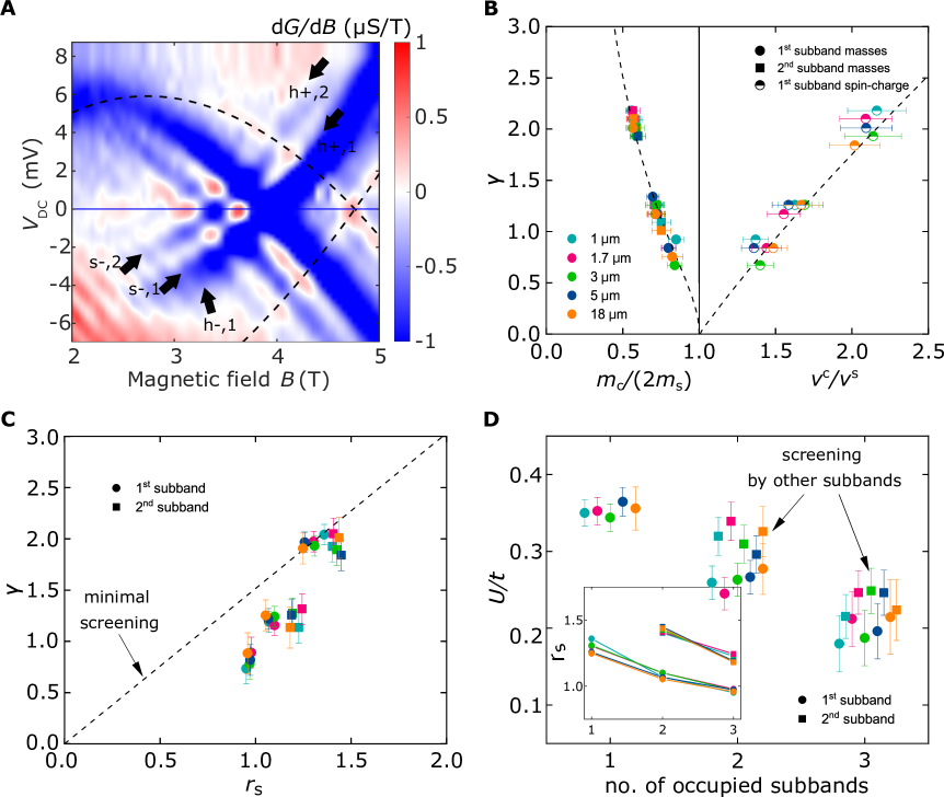
We have varied the number of occupied subbands all the way up to four, and fitted the bottom two using the model of two Fermi seas to extract the ratio of masses and velocities. Fitting the same data with the dispersion produced by the Hubbard model in a similar fashion to what was done before for the single-subband regime, see Fig. 2C, we obtain the values of that correspond to these ratios for each individual subband and for each subband occupancy in Fig. 4B, which allows the data points from multiple wires with a variety of densities (as seen in Fig. 2E) to be collapsed on to the same curve. The agreement between experiment and theory seen here further reinforces our claim of two separate Fermi seas for spinons and holons, having collected statistics belonging to five different devices, fabricated from two different wafers, across different fabrication cycles, and measured independently from one another in different cool-downs. Comparing the already extracted values of with for all measurements in Fig. 4C, we find that the two are approximately proportional to each other with a coefficient of . We interpret the still-observable discrepancy as a manifestation of the screening effect that is not captured by but is taken into account explicitly in the Hubbard model via the two-body interaction energy . The latter is proportional to the integral of the screened Coulomb potential, in which only the screening radius is changed in our experiment.
By means of the relation in Eq. (1) we extract the evolution of from the already obtained values of and as a function of the number of occupied subbands, as shown in Fig. 4D, for both the 1 and 2 lowest subbands, in different-length systems. Data corresponding to four occupied subbands was excluded, as its proximity to the non-interacting limit made the fitting less reliable. Similarly, fitting to the dispersions of the third and fourth subbands was not attempted owing to the lack of sharp features and overall increase in map complexity. Nevertheless, two clear trends emerge: first, decreases as more subbands are progressively filled, resulting in relative reductions of about % for the 1 subband and of % for the subband; second, the bottom subband seems to be systematically more strongly screened than the second, most likely due to their difference in density. These trends are also apparent in Fig. 4C, where the dashed line is drawn through the single-subband points and all further occupied subband systematically fall below it. We note that the values measured in the single-subband regime are consistent with the estimates made in (?), where the long-range Coulomb interaction between the electrons is screened by a conducting plate a certain distance away from the 1D wire. As far as the authors are aware, this is the first clear observation of screening effects between two 1D systems, with similar conclusions reported by (?) in 2D systems.
Discussion
We have shown that spin-charge separation is more robust than previously thought, extending past the low-energy regime of the TLL to beyond the Fermi energy. By tuning the degree of screening of the Coulomb interaction by changing the confinement in our wires and so the number of occupied subbands, we saw how the masses associated with the spin and charge Fermi seas evolve as a function of the interaction strength, with a remarkably good quantitative agreement with the predictions of the 1D Fermi-Hubbard model. At the same time, our comparison of quantum wires of different lengths confirms the prediction of the mode-hierarchy theory, observing systematically the emergence of at least two ‘replica’ modes as the wire length decreases.
Materials and Methods
Device fabrication
All tunnelling devices measured in this work were fabricated using double-quantum-well heterostructures, grown via molecular-beam epitaxy (MBE), comprised of two identical 18 nm GaAs quantum wells separated by a 14 nm Al0.165Ga0.835As superlattice tunnel barrier [10 pairs of Al0.33Ga0.67As and GaAs monolayers]. On each side of the barrier there were 40 nm Si-doped layers of Al0.33Ga0.67As (donor concentration ), with the lower and upper spacers being respectively 40 nm and 20 nm wide. Wafer 1, however, differed from Wafer 2 by having an additional 1002.5 mm/2.5 mm GaAs/AlGaAs superlattice below the 350 nm AlGaAs under the lower quantum well. This resulted in electron concentrations of about 3 (2.2) with mobilities of around 120 (165) in the top (bottom) well of Wafer 1, while 2.85 (1.54) and 191 (55) for Wafer 2, as measured at 1.4 K. A 10 nm GaAs cap layer was used to prevent oxidation. The distance from the upper well to the surface was 70 nm.
The electrical (surface) structure of the device was fabricated on a 200 m-wide Hall bar. Contacts to both layers were established using AuGeNi Ohmic contacts. Electron-beam lithography was used to define a split gate (SG), a mid-line gate (MG), a barrier gate (BG) and a cut-off gate (CG)—used in setting up the tunnelling conditions—together with an array of wire gates (WG)—used in defining the experimental 1D system (see Fig. 5A). The length of the wire gates was varied from 1–18 m. They were separated by 0.15–0.18 m gaps, and had a width of 0.1–0.3 m. A‘parasitic’ injection region also ran across the entire width of the mesa, with a fixed width of 0.45 m. A parasitic gate (PG) was used to modulate its density. All dimensions, particularly regarding the wire-region were carefully chosen in order to achieve minimal modulation of the lower-well carriers.
Momentum- and energy-resolved tunnelling spectroscopy
The tunnelling set-up was achieved as follows: first, the SG was negatively biased in order to pinch off both layers underneath, followed by positively biasing the MG in order to open a narrow conducting channel in the top well. At the other end of the device, the BG and the CG were biased enough to pinch off only the top layer. Under these conditions, any current injected through one of the Ohmic contacts had to have tunnelled between the layers in order to be detected (Fig. 5B).
Our spectroscopy technique consists of a low-noise, low-temperature measurement of the tunnelling current between the two 2D electron gas (2DEG) layers, which is given by (?)
| (2) |
where is the electron charge, is the Fermi-Dirac distribution function, is the centre-to-centre well separation, n is the unit normal to the 2D plane, is the magnetic-field vector, is the unit vector in the y-direction, and and are the spectral functions of the 1D and 2D systems respectively, with the corresponding Fermi energies being and . The tunnelling current between the two layers is then proportional to the overlap integral of their spectral functions. We induce an offset between the Fermi energies of the two systems by applying a DC bias between the layers. Similarly, an offset in momentum can also be obtained by applying a magnetic field of strength parallel to the 2DEG layers. When the field direction is along the (in-plane) -direction, the Lorentz force then shifts the momentum of the tunnelling electrons in the -direction by . Put together one can therefore map the dispersion of each system with respect to one another by measuring the differential conductance in both energy and momentum space.
References
- 1. T. Giamarchi, Quantum physics in one dimension (Clarendon press, Oxford, 2003).
- 2. S. Tomonaga, Remarks on Bloch’s method of sound waves applied to many-fermion problems. Prog. Theor. Phys. 5, 544 (1950).
- 3. J. M. Luttinger, An exactly soluble model of a many-fermion system. J. Math. Phys. 4, 1154 (1963).
- 4. F. D. M. Haldane, ’Luttinger liquid theory’ of one-dimensional quantum fluids. I. Properties of the Luttinger model and their extension to the general 1D interacting spinless Fermi gas. J. Phys. C 14, 2585-2609 (1981).
- 5. M. Bockrath, D. H. Cobden, J. Lu, A. G. Rinzler, R. E. Smalley, L. Balents, P. L. McEuen, Luttinger-liquid behaviour in carbon nanotubes. Nature 397, 598-601 (1999).
- 6. H. Ishii, H. Kataura, H. Shiozawa, H. Yoshioka, H. Otsubo, Y. Takayama, T. Miyahara, S. Suzuki, Y. Achiba, M. Nakatake, T. Narimura, M. Higashiguchi, K. Shimada, H. Namatame, M. Taniguchi, Direct observation of Tomonaga–Luttinger-liquid state in carbon nanotubes at low temperatures. Nature 426, 540-544 (2003).
- 7. Z. Shi, X. Hong, H. A. Bechtel, B. Zeng, M. C. Martin, K. Watanabe, T. Taniguchi, Y.-R. Shen, F. Wang, Observation of a Luttinger-liquid plasmon in metallic single-walled carbon nanotubes. Nat. Photonics 9, 515-519 (2015).
- 8. O. M. Auslaender, H. Steinberg, A. Yacoby, Y. Tserkovnyak, B. I. Halperin, K. W. Baldwin, L. N. Pfeiffer, K. W. West, Spin-charge separation and localization in one dimension. Science 308, 88-92 (2005).
- 9. Y. Jompol, C. J. B. Ford, J. P. Griffiths, I. Farrer, G. A. C. Jones, D. Anderson, D. A. Ritchie, T. W. Silk, A. J. Schofield, Probing spin-charge separation in a Tomonaga-Luttinger liquid. Science 325, 597-601 (2009).
- 10. D. Laroche, G. Gervais, M. P. Lilly, J. L. Reno, Positive and negative Coulomb drag in vertically integrated one-dimensional quantum wires. Nature Nanotechnology 6, 793–797 (2011).
- 11. B. J. Kim, H. Koh, E. Rotenberg, S.-J. Oh, H. Eisaki, N. Motoyama, S. Uchida, T. Tohyama, S. Maekawa, Z.-X. Shen, C. Kim, Distinct spinon and holon dispersions in photoemission spectral functions from one-dimensional SrCuO2. Nat. Phys. 2, 397-401 (2006).
- 12. J. Vijayan, P. Sompet, G. Salomon, J. Koepsell, S. Hirthe, A. Bohrdt, F. Grusdt, I. Bloch, C. Gross, Time-resolved observation of spin-charge deconfinement in fermionic Hubbard chains. Science 367, 186-189 (2020).
- 13. G. Barak, H. Steinberg, L. N. Pfeiffer, K. W. West, L. Glazman, F. von Oppen, A. Yacoby, Interacting electrons in one dimension beyond the Luttinger-liquid limit. Nat. Phys. 6, 489-493 (2010).
- 14. Y. Jin, O. Tsyplyatyev, M. Moreno, A. Anthore, W. K. Tan, J. P. Griffiths, I. Farrer, D. A. Ritchie, L. I. Glazman, A. J. Schofield, C. J. B. Ford, Momentum-dependent power law measured in an interacting quantum wire beyond the Luttinger limit. Nat. Commun. 10, 1-8 (2019).
- 15. S. Wang, S. Zhao, Z. Shi, F. Wu, Z. Zhao, L. Jiang, K. Watanabe, T. Taniguchi, A. Zettl, C. Zhou, F. Wang, Nonlinear Luttinger liquid plasmons in semiconducting single-walled carbon nanotubes. Nat. Mater. 19, 986-991 (2020).
- 16. A. Imambekov, L. I. Glazman, Universal theory of nonlinear Luttinger liquids. Science 323, 228-231 (2009).
- 17. T. L. Schmidt, A. Imambekov, L. I. Glazman, Fate of 1D spin-charge separation away from Fermi points. Phys. Rev. Lett. 104, 116403 (2010).
- 18. T. L. Schmidt, A. Imambekov, L. I. Glazman, Spin-charge separation in one-dimensional fermion systems beyond luttinger liquid theory. Phys. Rev. B 82, 245104 (2010).
- 19. O. Tsyplyatyev, A. J. Schofield, Y. Jin, M. Moreno, W. K. Tan, C. J. B. Ford, J. P. Griffiths, I. Farrer, G. A. C. Jones, D. A. Ritchie, Hierarchy of modes in an interacting one-dimensional system. Phys. Rev. Lett. 114, 196401 (2015).
- 20. O. Tsyplyatyev, A. J. Schofield, Y. Jin, M. Moreno, W. K. Tan, A. S. Anirban, C. J. B. Ford, J. P. Griffiths, I. Farrer, G. A. C. Jones, D. A. Ritchie, Nature of the many-body excitations in a quantum wire: Theory and experiment. Phys. Rev. B 93, 075147 (2016).
- 21. M. Moreno, C. J. B. Ford, Y. Jin, J. P. Griffiths, I. Farrer, G. A. C. Jones, D. A. Ritchie, O. Tsyplyatyev, A. J. Schofield, Nonlinear spectra of spinons and holons in short GaAs quantum wires. Nat. Commun. 7, 12784 (2016).
- 22. E. H. Lieb, F. Y. Wu, Absence of Mott transition in an exact solution of the short-range, one-band model in one dimension. Phys. Rev. Lett. 20, 1445-1448 (1968).
- 23. Y. Jin, M. Moreno, P. M. T. Vianez, W. K. Tan, J. P. Griffiths, I. Farrer, D. A. Ritchie, C. J. B. Ford, Microscopic metallic air-bridge arrays for connecting quantum devices. Appl. Phys. Lett. 118, 162108 (2021).
- 24. H. J. Schulz, Correlation exponents and the metal-insulator transition in the one-dimensional hubbard model. Phys. Rev. Lett. 64, 2831 -2834 (1990).
- 25. H. Frahm, V. E. Korepin, Critical exponents for the one-dimensional Hubbard model. Phys. Rev. B 42, 10553 (1990).
- 26. V. Meden, K. Schönhammer, Spectral functions for the Tomonaga-Luttinger model. Phys. Rev. B 46, 15753 -15760 (1992).
- 27. J. Voit, Charge-spin separation and the spectral properties of Luttinger liquids. Phys. Rev. B 47, 6740 -6743 (1993).
- 28. H. Benthien, F. Gebhard, E. Jeckelmann, Spectral Function of the One-Dimensional Hubbard Model away from Half Filling. Physical Review Letters 92, 256401 (2004).
- 29. G. D. Mahan, Many-Particle Physics (Plenum, New York, 1990).
- 30. B. Lake, D. A. Tennant, C. D. Frost, S. E. Nagler, Quantum criticality and universal scaling of a quantum antiferromagnet. Nat. Mater. 4, 329-334 (2005).
- 31. M. Mourigal, M. Enderle, A. Klöpperpieper, J.-S. Caux, A. Stunault, H. M. Rønnow, Fractional spinon excitations in the quantum Heisenberg antiferromagnetic chain. Nat. Phys. 9, 435-441 (2013).
- 32. B. Lake, D. A. Tennant, J.-S. Caux, T. Barthel, U. Schollwöck, S. E. Nagler, C. D. Frost, Multispinon continua at zero and finite temperature in a near-ideal Heisenberg chain. Phys. Rev. Lett. 111, 137205 (2013).
- 33. J.-S. Caux, J. M. Maillet, Computation of dynamical correlation functions of Heisenberg chains in a magnetic field. Phys. Rev. Lett. 95, 077201 (2005).
- 34. F. Göhmann, A. Klümper, A. Seel, Integral representations for correlation functions of the XXZ chain at finite temperature. J. Phys. A 37, 7625-7651 (2004).
- 35. A. Imambekov, T. L. Schmidt, L. I. Glazman, One-dimensional quantum liquids: Beyond the Luttinger liquid paradigm. Rev. Mod. Phys. 84, 1253 (2012).
- 36. F. H. L. Essler, Threshold singularities in the one-dimensional Hubbard model. Phys. Rev. B 81, 205120 (2010).
- 37. O. Tsyplyatyev, A. J. Schofield, Spectral-edge mode in interacting one-dimensional systems. Phys. Rev. B 90, 014309 (2014).
- 38. L. I. Glazman, I. M. Ruzin, B. I. Shklovskii, Quantum transport and pinning of a one-dimensional Wigner crystal. Phys. Rev. B 45, 8454–8463 (1992).
- 39. M. Kim, S. G. Xu, A. I. Berdyugin, A. Principi, S. Slizovskiy, N. Xin, P. Kumaravadivel, W. Kuang, M. Hamer, R. K. Kumar, R. V. Gorbachev, K. Watanabe, T. Taniguchi, I. V. Grigorieva, V. I. Fal’ko, M. Polini, A. K. Geim, Control of electron-electron interaction in graphene by proximity screening. Nat. Commun. 11, 2339 (2020).
Acknowledgements:
The authors would like to thank Leonid Glazman for assistance and helpful comments.
Funding: This work was supported by the UK EPSRC [Grant Nos. EP/J01690X/1 and EP/J016888/1]. P.M.T.V. acknowledges financial support from EPSRC International Doctoral Scholars studentship via grant number EP/N509620/1, and the EPSRC Doctoral Prize. O.T. was funded by the DFG [project No. 461313466].
Author Contributions P.M.T.V., Y.J., M.M., A.S.A, A.A. and W.K.T. fabricated the experimental devices, with P.M.T.V. and Y.J. performing the transport measurements shown. J.P.G. did the electron-beam lithography and I.F. and D.A.R. grew the heterostructure material.
P.M.T.V, O.T and C.J.B.F. analysed the data. O.T. and A.S. developed the theoretical framework. O.T. performed the calculations. C.J.B.F. supervised the experimental side of the project. All authors contributed to the discussion of the results. P.M.T.V., O.T. and C.J.B.F. wrote the manuscript.
Competing interests: Authors declare that they have no competing interests.
Data and materials availability: All data needed to evaluate the conclusions in the paper are present in the paper and/or the Supplementary Materials. The data and modelling code that support this work are also available at the University of Cambridge data repository (DOI: https://doi.org/10.17863/CAM.81347).