Topological phases in N-layer ABC-graphene boron-nitride moire superlattices
Abstract
Rhombohedral trilayer graphene on hexagonal boron nitride (TLG/BN) hosts gate-tunable, valley-contrasting, nearly flat topological bands that can trigger spontaneous quantum Hall phases under appropriate conditions of the valley and spin polarization. Recent experiments have shown signatures of C = 2 valley Chern bands at 1/4 hole filling, in contrast to the predicted value of C = 3. We discuss the low-energy model for rhombohedral N-layer graphene (N = 1, 2, 3) aligned with hexagonal boron nitride (hBN) subject to off-diagonal moire vector potential terms that can alter the valley Chern numbers. Our analysis suggests that topological phase transitions of the flat bands can be triggered by pseudomagnetic vector field potentials associated to moire strain patterns, and that a nematic order with broken rotational symmetry can lead to valley Chern numbers that are in agreement with recent Hall conductivity observations.
I Introduction
In recent years, magic-angle twisted bilayer graphene Bistritzer and MacDonald (2011); Cao et al. (2018a, b) (tBG) has emerged as a platform for exploring correlated insulating phases and unconventional superconductivity in compositionally simple systems, owing to the possibility of achieving extremely narrow bandwidths where Coulomb repulsion energies can dominate the kinetic energy of electrons. Bistritzer and MacDonald (2011); Wong et al. (2015); Cao et al. (2018a, b); Yankowitz et al. (2019); Cao et al. (2020); Serlin et al. (2019); Bultinck et al. (2020); Sharpe et al. (2019); Kim et al. (2017); Choi et al. (2019); Liu et al. (2019); Carr et al. (2018); Chittari et al. (2018a); Leconte et al. (2019); Zhao et al. (2020); Fidrysiak et al. (2018); Kang and Vafek (2019); Koshino et al. (2018); Tarnopolsky et al. (2019); Po et al. (2019); You and Vishwanath (2019); Park et al. (2019); Chichinadze et al. (2020); Shi et al. (2020); Crasto de Lima et al. (2019); Ma et al. (2020); Hesp et al. (2019); Fernandes and Venderbos (2020); Stepanov et al. (2020); Zhang et al. (2020); Song et al. (2019) The pool of moire materials exhibiting such behaviors has rapidly expanded beyond twisted bilayer graphene to include trilayer graphene on hexagonal boron nitride (TLG/BN), Chittari et al. (2019); Chen et al. (2019a, b, 2020); Yankowitz et al. (2016); Lin and Ni (2019); Yin et al. (2019); Zhang and Mao (2020); Kim et al. (2018); Repellin et al. (2020); Zhang and Senthil (2019); Abouelkomsan et al. (2020); Kindermann et al. (2012); Bokdam et al. (2014); San-Jose et al. (2014); Wallbank et al. (2013); Zhu et al. (2018) or double bilayer graphene (tDBG) Chebrolu et al. (2019); Liu et al. (2020); Lee et al. (2019); Shen et al. (2020); Choi and Choi (2019); Koshino (2019); Li et al. (2020); Zhang et al. (2019a) as representative systems where the perpendicular electric field can control the flatness of the low-energy moire bands and achieve the narrow bandwidths over a wider range of the twist angles, without requiring high-precision rotation as in tBG. Studies have evaluated the feasibility of engineering moire flat bands in gapped Dirac materials, Javvaji et al. (2020); kun Shi et al. (2020) suggesting TMDC bilayers Pan et al. (2018); Gong et al. (2014); Huang et al. (2014); Duan et al. (2014); Song and Gabor (2018) as platforms for identifying nearly flat bands where one can benefit from the aforementioned looser constraints on twist angle precision. Javvaji et al. (2020); Naik and Jain (2018); Wu et al. (2018, 2019); Jin et al. (2019a); Seyler et al. (2019); Bi and Fu (2019); Zhang et al. (2019b); Yu et al. (2019); Sushko et al. (2019); Tang et al. (2019); Jin et al. (2019b); An et al. (2019)
The finite valley Chern number of the moire bands underlie the anomalous Hall effects observed in transport experiments when the degeneracy of the bands are lifted via Coulomb interactions. Zhang et al. (2019a); Chittari et al. (2018b) Charge Hall conductivity signals were observed in twisted bilayer graphene nearly aligned with hexagonal boron nitride (tBG/BN) at 3/4 filling densities, Sharpe et al. (2019); Serlin et al. (2019) and closely related traces of quantum anomalous Hall effects were observed in TLG/BN. Chen et al. (2019a) Contrary to the expectations of a charge Hall conductivity of , which is consistent with the predicted valley Chern number of hole bands for TLG/BN, Chittari et al. (2018b) the experiments showed a quantized anomalous Hall conductivity of , which is consistent with . Chen et al. (2019a) In this paper we explore the valley Chern number phase diagram of G/BN, BG/BN, and ABC stacked TLG/BN structures, that can be described using the low-energy -chiral Dirac model subject to moire patterns, in an attempt to identify the system parameter conditions that can alter the valley Chern numbers. The manuscript is structured as follows. In Sec. II we introduce the model Hamiltonian, in Sec. III we present the electronic structure results comprising the valley Chern number phase diagrams, and lastly in Sec. IV we present the summary and discussions.
II Model Hamiltonian
The low-energy model Hamiltonian of rhombohedral -layer graphene on hexagonal boron nitride at the -valley subject to substrate moire patterns is given by Chittari et al. (2019)
| (1) |
where distinguishes the two possible (0∘ and 60∘) alignments between the layers of graphene and BN. The first term in equation (1) describes the low-energy N-layer graphene Hamiltonian containing the momentum operator , where is used for the principal valley of graphene, unless stated otherwise. The second term of equation (1) introduces the interlayer potential difference proportional to the mass term through . The third term, , describes the remote hopping term corrections for the N-layers. We model the remote hopping term corrections for TLG with , Jung as shown below:
The effective hopping parameters for rhombohedral trilayer graphene that fits the local density approximation (LDA) bands are eV, eV, eV, eV, and eV, where associated velocities are defined as , using as the lattice constant of graphene, and the constants in the diagonal terms are eV and eV.
In the case of , the parameters and drop out, and eV is used for bands obtained within the LDA Jung and MacDonald (2013) and the remote hopping terms are captured as
In the case of , all the remote hopping terms drop out and .
The last term of equation (1)
| (3) |
is the effective moire potential term induced by the hBN layer that consists of the diagonal and off-diagonal terms. We use the local commensurate stacking vector between the substrate and the contacting graphene layer, where the stacking vector and the real space position are related through
| (4) |
in the small angle approximation. Jung et al. (2014) Here, is the relative twist and is the lattice constant mismatch between the graphene and hBN layers, where and are the lattice constants of graphene and hBN layers respectively.
The diagonal term of the Hamiltonian in real space is given by
| (5) |
where the moire potential function is given by
| (6) |
which in turn depends on the auxiliary function
| (7) |
expressed using six moire reciprocal lattices successively rotated by 60∘. The moire reciprocal lattice vector is related to the following reciprocal lattice vector of graphene . For the diagonal terms of the moire potentials we use the parametrization of a G/BN interface Jung et al. (2014) projected onto only one of the sublattices. Chittari et al. (2019) The moire potential in Eq. (6) can be broken down in terms of inversion symmetric and asymmetric patterns, see Refs. [Wallbank et al., 2013; Jung et al., 2017] and appendix A for more details.
The intersublattice off-diagonal term introduces coherence between the low energy sublattices in the system and could arise in multilayer graphene with BN interfaced systems due to higher order perturbation corrections that couple the diagonal moire pattern terms with interlayer tunngling. This term can be modeled as
| (8) |
where is the Pauli matrix vector and the pseudomagnetic vector potential that we model through
| (9) |
where the prefactor
| (10) |
depends on twist angle and lattice constant mismatch
We will show that this off-diagonal vector potential in Eq. (8) can alter the Chern number phase diagram by breaking the rotational symmetry and modify the valley Chern numbers depending on system parameter values.
In a previous report Chittari et al. (2019) on the electronic structure of TLG/BN the moire potentials were modeled to act at the low energy sublattice of the contacting graphene layer and zero direct interlayer coherence between the low energy sites of the top and bottom layers was assumed by using zero off-diagonal term. There the proportionality to layer number was verified to up to three layers for either valence or conduction bands depending on the sign of the electric field and hBN substrate alignment orientation. As a matter of convention, in this work we assume that the valley Chern number is associated to the valley of the multilayer graphene layer while a time reversal symmetric counterpart is assumed for the counterpart. The zero or finite integer value of the valley Chern number in each band is attributed to the sum of the primary and secondary Chern weights typically concentrated near the gap opening points in the mBZ leading to the total valley Chern number, such that . While the primary Chern weight near charge neutrality is set by the interlayer potential difference, the secondary Chern weights near the mBZ boundaries depend on the moire potential parameters that generate the avoided secondary gaps at the mBZ corners. We will show in our analysis that the secondary Chern weights are easily altered based on the choice of the off-diagonal moire potential terms.
III Results and Discussions
Here we present the electronic structure of ABC multilayer graphene on hBN under the effect of an off-diagonal moire pattern term in Eq. (8) by allowing variations of the parameters between eV and for systems. We have verified that changing the diagonal moire parameters alone in a similar range of magnitude and phase did not modify the valley Chern numbers of the low energy bands which are 0 or . In the following we assess the impact of this term in particular in the valley Chern number of the low energy bands for fixed diagonal moire patterns and discuss the real-space anisotropies introduced in the local density of states.
III.1 Topological phase transitions in the low energy bands
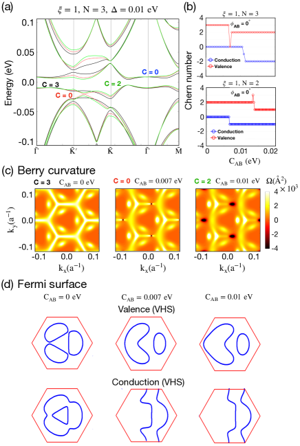
The main finding in this work is that the introduction of an off-diagonal interlayer coherence moire patterm term through a finite can switch the valley Chern number of the low energy bands in the system as we illustrate in Fig. 1, where the vector moire potential term defines a pseudospin field on the graphene layer contacting hBN.
The inclusion of off-diagonal terms causes significant changes in the electronic structure and triggers topological phase transitions, as shown in Fig. 1(a). The band structures for (TLG/BN) were obtained with with a constant value of interlayer potential difference eV. The continuous variation of the term with leads to a gap closure between the low energy valence band and the higher energy bands between and for a value of 0.007 eV, and the gap reopens for larger values of as shown in Fig. 1(a). Under the electric field, the gap at the primary Dirac point and the avoided gaps at the moire mini-Brillouin-zone (mBZ) boundaries isolate the low-energy bands near charge neutrality.
Introduction of a finite parameter also breaks the triangular rotational symmetry of the moire Brillouin zone that can be visualized in the Berry curvature distribution in Fig. 1(b). The Berry curvatures of the low energy low-energy bands are calculated through D. Xiao and Niu (2010)
| (11) |
where, for every -point, we obtain sums through all the neighboring bands; are the moire superlattice Bloch states, and are the eigenvalues. Based on the Berry curvature, the valley Chern number of the band is obtained from integrated in the moire Brillouin zone. The Berry curvatures for the valence band for three values of (before, after and at the transition) are compared in Fig. 1(b). Band closure between the low energy and higher energy bands is observed between moire Brillouin zone corners and , and is absent between another set of and in the mBZ. This asymmetry between the initially equivalent and or and mini-valleys indicates the rotational symmetry breaking introduced by the term.
The band closure as a function of indicates a possible topological transition of the bands. Indeed, the valley Chern number with has changed to after the band closure and re-opening. We present the low energy bands valley Chern numbers in Fig. 1(c), where the valley Chern number very near the band closure point ( = 0.007 eV) is . The conduction band valley Chern number undergoes a transition from to a non-zero valley Chern number as shown in Fig. 1 (c).
For hBN alignment and bilayer graphene (BG/BN) where we allow to change while keeping = 0 we see that the valence band exhibits a topological phase transition from to as shown in Fig. 1(d). However, for monolayer graphene aligned with hBN (G/BN) the valence band retains the same valley Chern number of even with increasing values of .
III.2 Broken rotational symmetry nematic local density of states
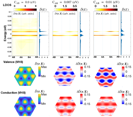
We had shown in Fig. 1 for a particular case of TLG/BN with and eV that the addition of an off-diagonal term in the moire Hamiltonian can trigger a topological phase transition. Here we report calculations of local density of states (LDOS) in order to distinguish how the added off-diagonal terms can modify the LDOS profile . In Fig. 2 we show the LDOS and density of states (DOS) for the low energy valence and conduction bands for theree values of , namely 0, 0.007, and 0.01 eV. The van Hove singularities in the DOS near the charge neutrality indicate the presence of flat bands. The conduction band has a localization at BA stacking, whereas the valence band has localization at AA stacking. With a finite off diagonal term the vHS peak is broadened slightly but the localization remains at the same stacking as illustrated in the LDOS plots. We use the normalized LDOS defined as /max in our plots and find the influence of off-diagonal moire term on the LDOS map through the difference . This quantity shows how the inclusion of a finite off-diagonal term leads to anisotropic LDOS profiles and breaks the triangular rotational symmetry of the solutions.
III.3 Pattern shape dependent Chern number phase diagrams
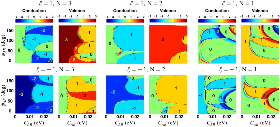
The moire pattern shapes that mix inversion symmetric and asymmetric components can be calibrated through the phase parameter that in turn controls the shapes of the triangular moire patterns in the first harmonic expansion, see the appendix for more details. In Fig. 1 we had noted the change in the valley Chern numbers with and combinations. However, there could be additional valley Chern number phases when is allowed to take a finite value. Indeed, we find this is the case and we have presented in Fig. 3 the valley Chern number phase diagram in the parameter space of eV and for TLG/BN, BG/BN and G/BN as concrete examples of -chiral systems up to three layers.
The results markedly depend on the orientation of the BN layer and for we generally obtain nonzero valley Chern number equal to while the conduction band is trivial with for . When we change the orientation of the substrate moire pattern by setting the conduction band becomes non-trivial acquiring an opposite sign valley Chern number , while the valence band acquires . It is noted that the valley Chern number of the valence/conduction bands are sensitive to both the off-diagonal parameters and provided that the former is sufficiently large and allows for additional valley Chern number transitions for both initially trivial and non-trivial bands.
In the case of TLG/BN, with , the valley Chern number of the valence (conduction) band is for = 0. The valley Chern number of the valence (conduction) band changed to for sufficiently large with = 0. For , the valley Chern number of valence (conduction) band is for = 0, and changed to with increasing value of .
Similarly, for BG/BN, with the valence (conduction) band has a phase transition from to . However, with , the valence/conduction band shows a transition from to .
For G/BN, with , the valence/conduction band has a valley Chern number . Even though the valley Chern number of the valence band did not change with increasing , the conduction band valley Chern number changed to . For the case of , the valence band valley Chern number remains unchanged while it does change for the conduction band when we modify .
IV Summary and discussion
We have explored the phase diagram map for the valley Chern numbers of the low energy valence and conduction bands of rhombohedral layer graphene boron-nitride superlattices for different moire patterns. The intra-sublattice diagonal moire patterns produces low energy bands whose valley Chern number magnitudes are zero or proportional to layer number . The absolute value of the maximum valley Chern number followed the number of graphene layers for all possible moire patterns within the first harmonic approximation. For zero off-diagonal patterns we find that the valence band has a valley Chern number equal to the number of layers when , while the conduction band is when .
However, introduction of off-diagonal interlayer coherence moire pattern terms captured through the magnitude and phase parameters allows to trigger topological phase transitions giving rise to valley Chern numbers that are smaller than the number of layers, a behavior that can be traced mainly to the variations in the electron-hole secondary Chern weights near the moire Brillouin zone boundaries. Thus, experimentally observed quantum anomalous Hall effects in TLG/BN Chen et al. (2019a) compatible with rather than the expected from layer number could result from rotational symmetry breaking interlayer coherence terms introduced by the Coulomb interactions. Our model off-diagonal contributions could also result from higher order corrections of the moire potentials mediated by interlayer tunneling. Broken rotational symmetry in the mBZ upon inclusion of off-diagonal terms in the Hamiltonian is evidenced from the Berry curvature distribution in momentum space and the LDOS maps.
In summary, we have presented valley Chern number phase diagrams in the parameter space that defines the off-diagonal moire pattern of the model Hamiltonian of rhombohedral -chiral multilayer graphene subject to moire scalar and vector potentials. The vector potential moire patterns which are often ignored in the low energy Hamiltonian models of -chiral multilayer graphene BN superlattices turned out to play a more prominent role than the scalar potentials for triggering topological transitions to phases with valley Chern numbers that are different to those dictated by layer number. Our results points to the possibility of triggering topological phase transitions by breaking the triangular rotational symmetry through pseudomagnetic field vector potentials generated by moire strain patterns. These can result for example from real strain fields whose bond distortions give rise to unequal electron hopping probabilities to the neighboring atoms, or from virtual effective strains due to high order interlayer electron hopping processes or Coulomb interactions.
Acknowledgements.
D.A.G.G. acknowledges partial support from the Universidad de Antioquia, Colombia, under initiative CODI ES84180154 Estrategia de sostenibilidad del Grupo de Física Atómica y Molecular and projects CODI-251594 and 2019-24770. Additionally, the authors are grateful to Professor Dr. Jorge Mahecha from the University of Antioquia for his advice and assistance in this work. We acknowledge financial support from the National Research Foundation of Korea (NRF) through grants NRF-2020R1A2C3009142 for B.L.C., NRF-2020R1A5A1016518 for Y. P., the Zhejiang Provincial Natural Science Foundation of China (Grant No. LY19A040003) for J. H. S., and the Basic study and Urban convergence R&D research fund of the University of Seoul (2019) for J. J. We acknowledge computational support from KISTI through grant KSC-2020-CRE-0072.References
- Bistritzer and MacDonald (2011) R. Bistritzer and A. H. MacDonald, Proceedings of the National Academy of Sciences 108, 12233 (2011).
- Cao et al. (2018a) Y. Cao, V. Fatemi, S. Fang, K. Watanabe, T. Taniguchi, E. Kaxiras, and P. Jarillo-Herrero, Nature 556, 43 (2018a).
- Cao et al. (2018b) Y. Cao, V. Fatemi, A. Demir, S. Fang, S. L. Tomarken, J. Y. Luo, J. D. Sanchez-Yamagishi, K. Watanabe, T. Taniguchi, E. Kaxiras, et al., Nature 556, 80 (2018b).
- Wong et al. (2015) D. Wong, Y. Wang, J. Jung, S. Pezzini, A. M. DaSilva, H.-Z. Tsai, H. S. Jung, R. Khajeh, Y. Kim, J. Lee, S. Kahn, S. Tollabimazraehno, H. Rasool, K. Watanabe, T. Taniguchi, A. Zettl, S. Adam, A. H. MacDonald, and M. F. Crommie, Phys. Rev. B 92, 155409 (2015).
- Yankowitz et al. (2019) M. Yankowitz, S. Chen, H. Polshyn, Y. Zhang, K. Watanabe, T. Taniguchi, D. Graf, A. F. Young, and C. R. Dean, Science 363, 1059 (2019).
- Cao et al. (2020) Y. Cao, D. Chowdhury, D. Rodan-Legrain, O. Rubies-Bigorda, K. Watanabe, T. Taniguchi, T. Senthil, and P. Jarillo-Herrero, Phys. Rev. Lett. 124, 076801 (2020).
- Serlin et al. (2019) M. Serlin, C. L. Tschirhart, H. Polshyn, Y. Zhang, J. Zhu, K. Watanabe, T. Taniguchi, L. Balents, and A. F. Young, Science (2019), 10.1126/science.aay5533.
- Bultinck et al. (2020) N. Bultinck, S. Chatterjee, and M. P. Zaletel, Phys. Rev. Lett. 124, 166601 (2020).
- Sharpe et al. (2019) A. L. Sharpe, E. J. Fox, A. W. Barnard, J. Finney, K. Watanabe, T. Taniguchi, M. A. Kastner, and D. Goldhaber-Gordon, 365, 605 (2019).
- Kim et al. (2017) K. Kim, A. DaSilva, S. Huang, B. Fallahazad, S. Larentis, T. Taniguchi, K. Watanabe, B. J. LeRoy, A. H. MacDonald, and E. Tutuc, Proceedings of the National Academy of Sciences 114, 3364 (2017).
- Choi et al. (2019) Y. Choi, J. Kemmer, Y. Peng, A. Thomson, H. Arora, R. Polski, Y. Zhang, H. Ren, J. Alicea, G. Refael, F. von Oppen, K. Watanabe, T. Taniguchi, and S. Nadj-Perge, Nature Physics 15, 1174 (2019).
- Liu et al. (2019) J. Liu, Z. Ma, J. Gao, and X. Dai, Phys. Rev. X 9, 031021 (2019).
- Carr et al. (2018) S. Carr, S. Fang, P. Jarillo-Herrero, and E. Kaxiras, Phys. Rev. B 98, 085144 (2018).
- Chittari et al. (2018a) B. L. Chittari, N. Leconte, S. Javvaji, and J. Jung, Electronic Structure 1, 015001 (2018a).
- Leconte et al. (2019) N. Leconte, S. Javvaji, J. An, and J. Jung, (2019), arXiv:1910.12805 [cond-mat.mes-hall] .
- Zhao et al. (2020) X.-J. Zhao, Y. Yang, D.-B. Zhang, and S.-H. Wei, Phys. Rev. Lett. 124, 086401 (2020).
- Fidrysiak et al. (2018) M. Fidrysiak, M. Zegrodnik, and J. Spałek, Phys. Rev. B 98, 085436 (2018).
- Kang and Vafek (2019) J. Kang and O. Vafek, Phys. Rev. Lett. 122, 246401 (2019).
- Koshino et al. (2018) M. Koshino, N. F. Q. Yuan, T. Koretsune, M. Ochi, K. Kuroki, and L. Fu, Phys. Rev. X 8, 031087 (2018).
- Tarnopolsky et al. (2019) G. Tarnopolsky, A. J. Kruchkov, and A. Vishwanath, Phys. Rev. Lett. 122, 106405 (2019).
- Po et al. (2019) H. C. Po, L. Zou, T. Senthil, and A. Vishwanath, Phys. Rev. B 99, 195455 (2019).
- You and Vishwanath (2019) Y.-Z. You and A. Vishwanath, npj Quantum Materials 4, 16 (2019).
- Park et al. (2019) M. J. Park, Y. Kim, G. Y. Cho, and S. Lee, Phys. Rev. Lett. 123, 216803 (2019).
- Chichinadze et al. (2020) D. V. Chichinadze, L. Classen, and A. V. Chubukov, Phys. Rev. B 101, 224513 (2020).
- Shi et al. (2020) H. Shi, Z. Zhan, Z. Qi, K. Huang, E. v. Veen, J. Á. Silva-Guillén, R. Zhang, P. Li, K. Xie, H. Ji, M. I. Katsnelson, S. Yuan, S. Qin, and Z. Zhang, Nature Communications 11, 371 (2020).
- Crasto de Lima et al. (2019) F. Crasto de Lima, R. H. Miwa, and E. Suárez Morell, Phys. Rev. B 100, 155421 (2019).
- Ma et al. (2020) C. Ma, Q. Wang, S. Mills, X. Chen, B. Deng, S. Yuan, C. Li, K. Watanabe, T. Taniguchi, X. Du, F. Zhang, and F. Xia, Nano Letters 20, 6076 (2020).
- Hesp et al. (2019) N. C. H. Hesp, I. Torre, D. Rodan-Legrain, P. Novelli, Y. Cao, S. Carr, S. Fang, P. Stepanov, D. Barcons-Ruiz, H. Herzig-Sheinfux, K. Watanabe, T. Taniguchi, D. K. Efetov, E. Kaxiras, P. Jarillo-Herrero, M. Polini, and F. H. L. Koppens, (2019), arXiv:1910.07893 [cond-mat.str-el] .
- Fernandes and Venderbos (2020) R. M. Fernandes and J. W. F. Venderbos, Science Advances 6 (2020), 10.1126/sciadv.aba8834.
- Stepanov et al. (2020) P. Stepanov, I. Das, X. Lu, A. Fahimniya, K. Watanabe, T. Taniguchi, F. H. L. Koppens, J. Lischner, L. Levitov, and D. K. Efetov, Nature 583, 375 (2020).
- Zhang et al. (2020) Y. Zhang, Y. Gao, and D. Xiao, Phys. Rev. B 101, 041410 (2020).
- Song et al. (2019) Z. Song, Z. Wang, W. Shi, G. Li, C. Fang, and B. A. Bernevig, Phys. Rev. Lett. 123, 036401 (2019).
- Chittari et al. (2019) B. L. Chittari, G. Chen, Y. Zhang, F. Wang, and J. Jung, Phys. Rev. Lett. 122, 016401 (2019).
- Chen et al. (2019a) G. Chen, A. L. Sharpe, P. Gallagher, I. T. Rosen, E. J. Fox, L. Jiang, B. Lyu, H. Li, K. Watanabe, T. Taniguchi, J. Jung, Z. Shi, D. Goldhaber-Gordon, Y. Zhang, and F. Wang, Nature 572, 215 (2019a).
- Chen et al. (2019b) G. Chen, L. Jiang, S. Wu, B. Lyu, H. Li, B. L. Chittari, K. Watanabe, T. Taniguchi, Z. Shi, J. Jung, Y. Zhang, and F. Wang, Nature Physics 15, 237 (2019b).
- Chen et al. (2020) G. Chen, A. L. Sharpe, E. J. Fox, Y.-H. Zhang, S. Wang, L. Jiang, B. Lyu, H. Li, K. Watanabe, T. Taniguchi, Z. Shi, T. Senthil, D. Goldhaber-Gordon, Y. Zhang, and F. Wang, Nature 579, 56 (2020).
- Yankowitz et al. (2016) M. Yankowitz, K. Watanabe, T. Taniguchi, P. San-Jose, and B. J. LeRoy, Nature communications 7, 13168 (2016).
- Lin and Ni (2019) X. Lin and J. Ni, Phys. Rev. B 100, 195413 (2019).
- Yin et al. (2019) L.-J. Yin, L.-J. Shi, S.-Y. Li, Y. Zhang, Z.-H. Guo, and L. He, Phys. Rev. Lett. 122, 146802 (2019).
- Zhang and Mao (2020) Y.-H. Zhang and D. Mao, Phys. Rev. B 101, 035122 (2020).
- Kim et al. (2018) H. Kim, N. Leconte, B. L. Chittari, K. Watanabe, T. Taniguchi, A. H. MacDonald, J. Jung, and S. Jung, Nano Letters 18, 7732 (2018).
- Repellin et al. (2020) C. Repellin, Z. Dong, Y.-H. Zhang, and T. Senthil, Phys. Rev. Lett. 124, 187601 (2020).
- Zhang and Senthil (2019) Y.-H. Zhang and T. Senthil, Phys. Rev. B 99, 205150 (2019).
- Abouelkomsan et al. (2020) A. Abouelkomsan, Z. Liu, and E. J. Bergholtz, Phys. Rev. Lett. 124, 106803 (2020).
- Kindermann et al. (2012) M. Kindermann, B. Uchoa, and D. L. Miller, Phys. Rev. B 86, 115415 (2012).
- Bokdam et al. (2014) M. Bokdam, T. Amlaki, G. Brocks, and P. J. Kelly, Phys. Rev. B 89, 201404 (2014).
- San-Jose et al. (2014) P. San-Jose, A. Gutiérrez-Rubio, M. Sturla, and F. Guinea, Phys. Rev. B 90, 075428 (2014).
- Wallbank et al. (2013) J. R. Wallbank, A. A. Patel, M. Mucha-Kruczyński, A. K. Geim, and V. I. Fal’Ko, Phys. Rev. B 87, 1 (2013).
- Zhu et al. (2018) G.-Y. Zhu, T. Xiang, and G.-M. Zhang, Science Bulletin 63, 1087 (2018).
- Chebrolu et al. (2019) N. R. Chebrolu, B. L. Chittari, and J. Jung, Phys. Rev. B 99, 235417 (2019).
- Liu et al. (2020) X. Liu, Z. Hao, E. Khalaf, J. Y. Lee, Y. Ronen, H. Yoo, D. Haei Najafabadi, K. Watanabe, T. Taniguchi, A. Vishwanath, and P. Kim, Nature 583, 221 (2020).
- Lee et al. (2019) J. Y. Lee, E. Khalaf, S. Liu, X. Liu, Z. Hao, P. Kim, and A. Vishwanath, Nature Communications 10, 5333 (2019).
- Shen et al. (2020) C. Shen, Y. Chu, Q. Wu, N. Li, S. Wang, Y. Zhao, J. Tang, J. Liu, J. Tian, K. Watanabe, T. Taniguchi, R. Yang, Z. Y. Meng, D. Shi, O. V. Yazyev, and G. Zhang, Nature Physics 16, 520 (2020).
- Choi and Choi (2019) Y. W. Choi and H. J. Choi, Phys. Rev. B 100, 201402 (2019).
- Koshino (2019) M. Koshino, Phys. Rev. B 99, 235406 (2019).
- Li et al. (2020) X. Li, F. Wu, and S. Das Sarma, Phys. Rev. B 101, 245436 (2020).
- Zhang et al. (2019a) Y.-H. Zhang, D. Mao, Y. Cao, P. Jarillo-Herrero, and T. Senthil, Phys. Rev. B 99, 075127 (2019a).
- Javvaji et al. (2020) S. Javvaji, J.-H. Sun, and J. Jung, Phys. Rev. B 101, 125411 (2020).
- kun Shi et al. (2020) L. kun Shi, J. Ma, and J. C. W. Song, 2D Materials 7, 015028 (2020).
- Pan et al. (2018) Y. Pan, S. Fölsch, Y. Nie, D. Waters, Y.-C. Lin, B. Jariwala, K. Zhang, K. Cho, J. A. Robinson, and R. M. Feenstra, Nano letters 18, 1849 (2018).
- Gong et al. (2014) Y. Gong, J. Lin, X. Wang, G. Shi, S. Lei, Z. Lin, X. Zou, G. Ye, R. Vajtai, B. I. Yakobson, et al., Nature materials 13, 1135 (2014).
- Huang et al. (2014) C. Huang, S. Wu, A. M. Sanchez, J. J. Peters, R. Beanland, J. S. Ross, P. Rivera, W. Yao, D. H. Cobden, and X. Xu, Nature materials 13, 1096 (2014).
- Duan et al. (2014) X. Duan, C. Wang, J. C. Shaw, R. Cheng, Y. Chen, H. Li, X. Wu, Y. Tang, Q. Zhang, A. Pan, et al., Nature nanotechnology 9, 1024 (2014).
- Song and Gabor (2018) J. C. W. Song and N. M. Gabor, Nature Nanotechnology 13, 986 (2018).
- Naik and Jain (2018) M. H. Naik and M. Jain, Phys. Rev. Lett. 121, 266401 (2018).
- Wu et al. (2018) F. Wu, T. Lovorn, E. Tutuc, and A. H. MacDonald, Phys. Rev. Lett. 121, 026402 (2018).
- Wu et al. (2019) F. Wu, T. Lovorn, E. Tutuc, I. Martin, and A. H. MacDonald, Phys. Rev. Lett. 122, 086402 (2019).
- Jin et al. (2019a) C. Jin, E. C. Regan, A. Yan, M. Iqbal Bakti Utama, D. Wang, S. Zhao, Y. Qin, S. Yang, Z. Zheng, S. Shi, K. Watanabe, T. Taniguchi, S. Tongay, A. Zettl, and F. Wang, Nature 567, 76 (2019a).
- Seyler et al. (2019) K. L. Seyler, P. Rivera, H. Yu, N. P. Wilson, E. L. Ray, D. G. Mandrus, J. Yan, W. Yao, and X. Xu, Nature 567, 66 (2019).
- Bi and Fu (2019) Z. Bi and L. Fu, (2019), arXiv:1911.04493 [cond-mat.str-el] .
- Zhang et al. (2019b) L. Zhang, Z. Zhang, F. Wu, D. Wang, R. Gogna, S. Hou, K. Watanabe, T. Taniguchi, K. Kulkarni, T. Kuo, S. R. Forrest, and H. Deng, (2019b), arXiv:1911.10069 [cond-mat.mes-hall] .
- Yu et al. (2019) H. Yu, M. Chen, and W. Yao, National Science Review (2019), 10.1093/nsr/nwz117.
- Sushko et al. (2019) A. Sushko, K. D. Greve, T. I. Andersen, G. Scuri, Y. Zhou, J. Sung, K. Watanabe, T. Taniguchi, P. Kim, H. Park, and M. D. Lukin, (2019), arXiv:1912.07446 [cond-mat.mes-hall] .
- Tang et al. (2019) Y. Tang, L. Li, T. Li, Y. Xu, S. Liu, K. Barmak, K. Watanabe, T. Taniguchi, A. H. MacDonald, J. Shan, and K. F. Mak, (2019), arXiv:1910.08673 [cond-mat.mtrl-sci] .
- Jin et al. (2019b) C. Jin, E. C. Regan, D. Wang, M. Iqbal Bakti Utama, C.-S. Yang, J. Cain, Y. Qin, Y. Shen, Z. Zheng, K. Watanabe, T. Taniguchi, S. Tongay, A. Zettl, and F. Wang, Nature Physics 15, 1140 (2019b).
- An et al. (2019) L. An, X. Cai, M. Huang, Z. Wu, J. Lin, Z. Ying, Z. Ye, X. Feng, and N. Wang, (2019), arXiv:1907.03966 [cond-mat.mes-hall] .
- Chittari et al. (2018b) B. L. Chittari, N. Leconte, S. Javvaji, and J. Jung, Electronic Structure 1, 015001 (2018b).
- (78) J. Jung, Unpublished .
- Jung and MacDonald (2013) J. Jung and A. H. MacDonald, Phys. Rev. B 87, 195450 (2013).
- Jung et al. (2014) J. Jung, A. Raoux, Z. Qiao, and A. H. MacDonald, Phys. Rev. B 89, 205414 (2014).
- Jung et al. (2017) J. Jung, E. Laksono, A. M. DaSilva, A. H. MacDonald, M. Mucha-Kruczyński, and S. Adam, Phys. Rev. B 96, 085442 (2017).
- D. Xiao and Niu (2010) M.-C. C. D. Xiao and Q. Niu, Rev. Mod. Phys. 82, 1959 (2010).
Appendix A Inversion symmetric and asymmetric moire patterns
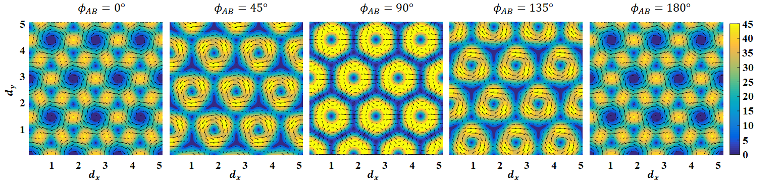
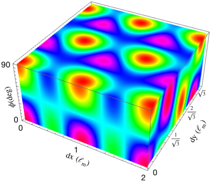
Here we discuss in more detail the breakdown of the moire patterns into inversion symmetric and asymmetric terms Wallbank et al. (2013) for the diagonal scalar moire pattern in Eq. (5) and off-diagonal vector potential-like term in Eq. (8). Illustrations of the diagonal and off-diagonal moire patterns for different phase angles are in Fig. 4.
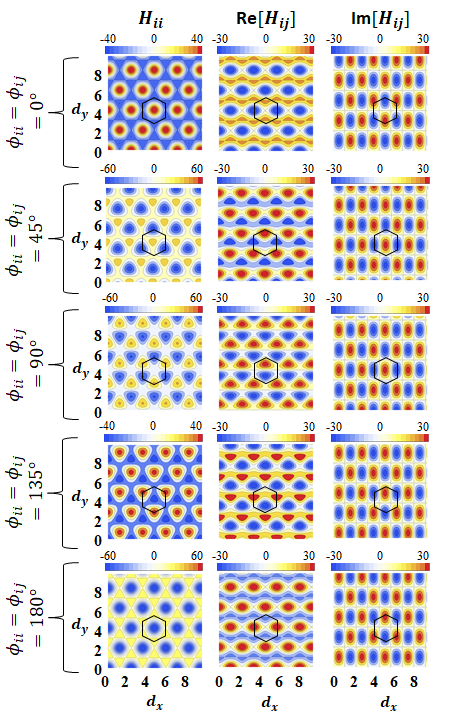
The diagonal element of the moire potential in Eq. (5) involving a scalar function is defined in terms of and for we have
with (symmetric function) and (antisymmetric function), where we use six moire reciprocal lattices successively rotated by 60∘ as introduced in the main text. Hence, the moire pattern in Eq. (A) will be symmetric for and asymmetric when for integer values, and a combination of both for intermediate phase angles. In Fig. 5, we illustrate the patterns in real space for different values of the angle .
The off-diagonal term with given in Eq. (8) has a vector potential term defined in Eq. (A) that can be represented by its magnitude and orientation as in Fig. 6,