Fabry-Perot Interferometric Calibration of 2D Nanomechanical Plate Resonators
Abstract
Displacement calibration of nanomechanical plate resonators presents a challenging task. Large nanomechanical resonator thickness reduces the amplitude of the resonator motion due to its increased spring constant and mass, and its unique reflectance. Here, we show that the plate thickness, resonator gap height, and motional amplitude of circular and elliptical drum resonators, can be determined in-situ by exploiting the fundamental interference phenomenon in Fabry-Perot cavities. The proposed calibration scheme uses optical contrasts to uncover thickness and spacer height profiles, and reuse the results to convert the photodetector signal to the displacement of drumheads that are electromotively driven in their linear regime. Calibrated frequency response and spatial mode maps enable extraction of the modal radius, effective mass, effective driving force and Young’s elastic modulus of the drumhead material. This scheme is applicable to any configuration of Fabry-Perot cavities, including plate and membrane resonators.
Nanomechanical resonators (NMRs) are exceptional force and mass sensors[1, 2], which made them valuable test platforms for the investigation of various phenomena at the nanoscale such as synchronization[3, 4], noise[5, 6], nonlinearity[7, 8], and light-matter interaction[9, 10, 11]. NMRs with flexural modes (i.e. plates and beams) have attracted interest due to their linear response even to large deformation-inducing forces[12, 13]. The well-known mechanical properties of the bulk material and its geometry determine plate and beam frequencies that can be predicted to a high accuracy. This allows the realization of unique device applications such as nanomechanical mass spectrometers[14, 15], phononic crystals built from NMR arrays[16, 17], and complex networks of NMRs embedded in electrical circuits[3, 4], and cavity-mediated quantum systems[18].
Calibration of NMR displacement is important for quantification of device characteristics in sensing applications. While the spatial dynamics of membrane NMRs, whose behavior is to a large extent determined by tensile stress, have been investigated in great detail with optical interferometry[19, 20, 21, 8], plate NMRs have been less explored. Studies involving Fabry-Perot (FP) cavities have introduced calibration of the vibrational amplitudes of membrane and string NMRs[22, 20, 23, 24]. However, they are hardly applicable to plate NMRs because of reduced vibrational amplitudes owing to the increased spring constant and mass, and unique reflectance versus FP cavity length arising from thick absorptive materials such as niobium diselenide. Also, there are cases where a smaller spacing is preferred over the optimal spacing for interferometric detection. These cases include mechanical frequency tuning by low gate voltages[25, 26, 27], and stronger electomechanical coupling between mechanical resonators and microwave cavities[28, 29].
In this Letter, we show that the motion of plate NMRs can be calibrated by considering multilayer wave interferences occurring on the FP structure. To demonstrate the robustness of the technique, a thick 2D material, NbSe2, is used as the drumhead. This approach allows determination of the layer thickness, spacer height and device responsivity of each translucent flexible mirror. Our calibration scheme reveals subnanometer mechanical displacements for the measured response of plate NMRs with thickness exceeding 50 nm.
Figure 1(a) shows Device A, a circular plate with a hole diameter of 7m, and Device B, an elliptical plate with hole diameters of 8m (X, major axis) and 7m (Y, minor axis). The devices share the same flake, ground electrode, and driving voltages. The NbSe2 flake and ground electrodes are separated by the insulating layer (electron-beam resist CSAR-62) and vacuum spacers, and hence form FP cavities for detection, and capacitors for actuation. A large rectangular opening, located tens of microns below the drum centers, allows the flake to connect to the voltage-controlled Au/Cr electrodes. The motion of the electromotively driven plates is detected interferometrically in a high vacuum environment[30].

Our method relies on different contrast of light elastically reflected from each zone, as shown in Fig. 1(b). The flake (pink bar) acts as a translucent movable mirror with thickness , which is separated from the ground electrode by a spacer of height . For convenience, the reflected intensity is expressed in terms of the reflectance , which is the ratio of the total reflected light intensity to the incident intensity. Stationary mirrors have only DC component while movable mirrors have both and AC component . Zones 1 and 2 represent two stationary mirrors: stacks of gold, orange, green and blue bars having reflectance and a mirror covered with a spacer (light gray) having reflectance , respectively. Zone 3 represents two stationary mirrors separated by a dielectric gap (clamp) with reflectance . Finally, zone 4 is the main FP cavity composed of one stationary and one movable mirrors, which are separated by a vacuum gap with reflectance . Here, zones 1 and 2 are references for zones 4 and 3, respectively. Scanning mirrors in the measurement setup move the laser spot in each zone a distance and away from the drums’ center.
Application of DC and AC voltages to the flake exerts an attractive force; the NMR responds with an out-of-plane motional amplitude at a driving frequency . Due to the position and motion of the movable mirror in zone 4, the main FP cavity has reflectance , with . Figure 1(d) shows the photodetector output signal acquired from . Both the DC component and the AC component of the output signal are proportional to and , respectively. Amplitude is determined after obtaining and .
Though we calculate using the multilayer interference approach[31, 32, 33] (MIA), the reflectance of FP cavities with four interfaces[34, 35] captures the stationary reflections occurring for each drum. Here, we assume that the coherent probe light, having wavelength , originates from a point source and propagates from a semi-infinite vacuum layer. The drum and the bottom mirror have complex refractive indices [36] and , respectively, whereas the spacers have real refractive index ( for the vacuum spacer and for the CSAR-62 spacer). In this geometry, the vacuum-NMR, NMR-spacer, and spacer-mirror interfaces contribute significantly to the cavity’s overall reflectance. The total reflectance is defined as
| (1) |
where is the optical phase thickness of the NMR, is the optical phase thickness of the spacer, = is the Fresnel coefficient of the vacuum-NMR interface, = is the Fresnel coefficient of the NMR-spacer interface, and is the equivalent Fresnel coefficient of the spacer-mirror interface. For convenience, is computed using MIA[30].
Figure 1(c) shows the topographical features of the drum devices as probed by a continuous wave laser beam. Apparently, the reflectance signal measured along the white dashed lines drawn across devices A and B contains , taken outside the dashed ellipses, and , taken within the dashed ellipses. Polygons 1 and 2 give average values of and . The colored dashed ellipses, representing the hole diameters measured in Fig. 1(a), are smaller than the light gray ellipses. These gray ellipses manifest in Fig. 1(a) as concentric purple rings seen for each drum. These features arise when the flake transfer, that is based on elastomeric stamps, deforms the edge of every drum hole.
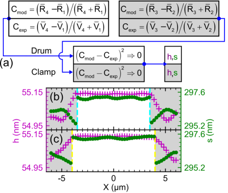
Since is susceptible to scattering losses[37], we circumvent this issue by normalizing the Michelson contrast[34] of each FP cavity to their reference. Having defined the experimental and calculated reflectance, the cavity’s optical contrast, , is quantified as , where is the stationary reflectance of the FP cavity, and is the stationary reflectance of the cavity’s reference. Apparently, ranges between -1 and 1, with zero denoting no difference with the reference. If is positive, then the cavity is brighter than the reference. Otherwise, the cavity is darker than its reference.
The output voltages measured for each pixel along the dashed lines in Fig. 1(c) are converted into contrast values for devices A and B, as depicted in Fig. 2(a). The experimental contrast represents the ratio of voltages acquired from different zones in the confocal image of each device while the modelled contrast is derived using MIA[30]. Figures 2(b-c) show the resulting and cross-section profiles acquired from minimizing the difference between the experimental contrast values and the contrasts generated by MIA. The mean plate thicknesses and spacer heights for the two devices are in excellent agreement with the mean values listed in Table 1. The spacer height for both drums and clamps agrees well with the stylus profilometer measurements. From the flake thickness of about 55 nm, we deduce 92 layers of NbSe2 sheets assuming a single layer thickness of nm[38].
| Devices | A | B |
| (nm) | 55.139 0.002 | 55.135 0.002 |
| (nm) | 55.03 0.05 | 55.05 0.04 |
| (nm) | 297.2 0.1 | 297.3 0.1 |
| (nm) | 296.0 0.3 | 295.9 0.3 |
The profiles in Figs. 2(b-c) show a hundred picometer variation between the drum and clamp zones. Meanwhile, buckling is observed in the profiles in Figs. 2(b-c) as for both devices are greater than by nm. We see the drumheads bulge[39, 40] presumably due to the pressure difference between the trapped air in the drum hole and the vacuum environment. The surface roughness of the movable mirror likely comes from the thermally-grown oxide[41] on the surface of the stationary mirror.
Having determined the mean and , we evaluate the optical reflectance-to-displacement responsivity of each drum. This quantity is obtained from = . The AC component reflected from zone 4 and characterized by , being purely due to mechanical motion, is insensitive to any scattering losses as this wave is amplitude-modulated. Eq. (1) is then corrected by a prefactor that accounts for the finite spot size of the probe Gaussian beam[30].
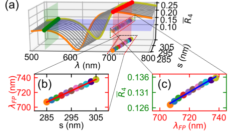
We define the average to account for spatial variations in across the plate due to the pressure difference and DC voltage. Note that each complex-valued refractive index is dependent on the probing wavelength; this translates into the wavelength-dependent , and . We modeled by the chain rule , where is the change of with regards to the wavelength shift in the FP cavity, and is the wavelength shift of the FP cavity caused by the change of the spacer gap. The resulting dependences are shown as a waterfall plot in Fig. 3(a) with a gap range exceeding the uncertainty of our stylus profilometer[30]. Figure 3(a) demonstrates larger at near-infrared wavelengths. Figure 3(b) shows the peak wavelength of the cavity, falling in the near-infrared range, shifting linearly with a slope of nm/nm as increases from nm to nm. Figure 3(c) shows how the shift consequently increases linearly, with a slope of nm-1. The product of these two slopes, nm-1, agrees with nm-1 that is evaluated from the gradient of the with respect to [30]. The linear behavior seen in Figs. 3(b-c) is in contrast to the non-linear dependence observed for optically-thin membranes in the same ranges of [30].
We use the average responsivity together with the interferometer system gain () (V/W), and the laser probe power to define the displacement amplitude as
| (2) |
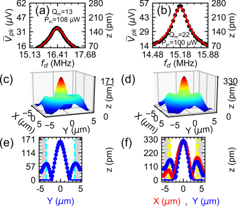
where is the frequency and position-dependent peak voltage response of the NMR. The denominator in Eq. (2), when squared, represents the transduction factor (in V2/m2) that one can deduce from the measured Brownian motion of a mechanical resonator probed by an interferometric system[22, 20]. This quantity accounts for the device responsivity and the detection parameters in the interferometric setup[30]. We deduce transduction factors of V/pm for device A, and V/pm for device B for probe powers listed in Figs. 4(a-b).
Figures 4(a-b) show the measured voltage response and its corresponding for devices A and B. The measured response profile agrees well with a driven mechanical resonator model in the linear regime[42]:
| (3) |
where is the fundamental mode frequency, is the mode quality factor, and is the amplitude expressed as effective acceleration. is the mode shape of the plate described as
| (4) |
where and are the zeroth Bessel and modified Bessel functions of the first kind, respectively, is the fundamental mode constant for a clamped circular plate, and is a normalization constant. Here, represents the normalized coordinates away from the maximum of , where and represent the NMR major (X axis) and minor (Y axis) modal radii, respectively. By setting , we measure pm for device A, and pm for device B. Their magnitudes are three orders of magnitude smaller than and .
| Specifications | Device A | Device B | Method |
| (pm) | 161 | 320 | Eq. (4) |
| (m) | 2.7 0.2 | 3.19 0.06 | Eq. (4) |
| (m) | 2.6 0.2 | 2.66 0.02 | Eq. (4) |
| (fg) | 1.4 | 1.74 | [30] |
| (km/s2) | 132 | 132 | Eq. (3) |
| (pN) | 191 | 229 | [30] |
| (GPa) | 135 13 | [30] | |
By driving the plates at , and probing their spatial mode shape with scanning mirrors, we observe surface plots of for devices A and B as shown in Figs. 4(c-d). Figures 4(e-f) show X and Y axes cuts, with both axes intersecting at of Figs. 4(c-d). They reveal profiles that agree with Eq. (4), with and acting as free parameters. , , and of the two plates are listed in Table 2. The discrepancy in the values of and of device B is due to the location of the laser spot that probed Fig. 4(b). Whereas lies at 0, lies at m away from the spatial peak. Both and for devices A and B are smaller than the hole radii (set as cyan and yellow dashed lines in Figs. 4(e-f)), making for both devices higher than the designed values. Moreover, device A shows unexpected elliptical modal behavior with a miniscule difference between and , which is due to the fabrication process.
Table 2 lists other NMR-related quantities that are derived from Figure 4 such as the effective mass , acceleration , force , and Young’s elastic modulus . These quantities are derived from a clamped elliptical plate model[30]. The estimated is within the range of reported values for bulk NbSe2 flakes[43, 44]. These quantities are obtained without inducing damage on the flake, and are independent of the actuation scheme.
Eq. (4) does not explain the asymmetric sinusoidal waves propagating beyond the drum edges seen in Figs. 4(e-f). These waves are signatures of support losses due to imperfect flake clamping at the edges[45]. Discussing the waves’ origin goes beyond the scope of this study, though resolving the waves’ amplitude, which is of , demonstrate the capability of our method to visualize acoustic waves in NMRs [17].
In summary, we demonstrated an in-situ, non-invasive method of calibrating motional displacement of plate NMRs by exploiting wave interference phenomena in FP cavities. Using a probe laser beam, and applying MIA to different realizations, we determine cross-sectional profiles of the NMR thickness and spacer height, transduction factors of NbSe2 plate resonators, and subnanometer motional amplitudes that helped examine modal properties of the drumheads. We foresee that this method will be applicable to flexural and acoustic wave resonators of various geometries.
Acknowledgements.
We acknowledge the contributions of T.-H. Hsu and W.-H. Chang in fabricating devices and in building the experimental setup. We thank A.F. Rigosi for sharing the measured dielectric constant spectra of bulk and few-layers of NbSe2. We thank the Taiwan International Graduate Program for the financial support. This project is funded by Academia Sinica Grand Challenge Seed Program (AS-GC-109-08), Ministry of Science and Technology (MOST) of Taiwan (107-2112-M-001-001-MY3), Cost Share Programme (107-2911-I-001-511), the Royal Society International Exchanges Scheme (grant IESR3170029), and iMATE(2391-107-3001). We extend our gratitude for the Academia Sinica Nanocore Facility. Attributions.-M.A.C.A. and J.C.E. contributed equally in this work. C.-D.C. conceived the devices and supervised the project; J.C.E. fabricated the devices. M.A.C.A. and J.-Y.W. modeled the calibration scheme. C.-Y.Y. and K.-H.L. designed and built the setup for optical measurements. M.A.C.A., J.C.E. and C.-Y.Y. performed the experiment. M.A.C.A., J.C.E., J.-Y.W., T.-H.L., K.-S.C.-L., S.K., Y.P. and C.-D.C. analyzed the data, performed simulations and wrote the manuscript; all authors discussed the results and contributed to the manuscript.References
- Ekinci and Roukes [2005] K. L. Ekinci and M. L. Roukes, Nanoelectromechanical Systems, Rev. Sci. Instrum. 76, 10.1063/1.1927327 (2005).
- Imboden and Mohanty [2014] M. Imboden and P. Mohanty, Dissipation in Nanoelectromechanical Systems, Phys. Rep. 534, 89 (2014).
- Fon et al. [2017] W. Fon, M. H. Matheny, J. Li, L. Krayzman, M. C. Cross, R. M. D’Souza, J. P. Crutchfield, and M. L. Roukes, Complex Dynamical Networks Constructed with Fully Controllable Nonlinear Nanomechanical Oscillators, Nano. Lett. 17, 5977 (2017).
- Matheny et al. [2019] M. H. Matheny, J. Emenheiser, W. Fon, A. Chapman, A. Salova, M. Rohden, J. Li, M. Hudoba de Badyn, M. Posfai, L. Duenas-Osorio, M. Mesbahi, J. P. Crutchfield, M. C. Cross, R. M. D’Souza, and M. L. Roukes, Exotic States in a Simple Network of Nanoelectromechanical Oscillators, Science 363, 1057 (2019).
- Cleland and Roukes [2002] A. N. Cleland and M. L. Roukes, Noise Processes in Nanomechanical Resonators, J. Appl. Phys. 92, 2758 (2002).
- Maillet et al. [2018] O. Maillet, X. Zhou, R. R. Gazizulin, R. Ilic, J. M. Parpia, O. Bourgeois, A. D. Fefferman, and E. Collin, Measuring Frequency Fluctuations in Nonlinear Nanomechanical Resonators, ACS Nano 12, 5753 (2018).
- Davidovikj et al. [2017] D. Davidovikj, F. Alijani, S. J. Cartamil-Bueno, H. S. van der Zant, M. Amabili, and P. G. Steeneken, Nonlinear Dynamic Characterization of Two-Dimensional Materials, Nat. Commun. 8, 1 (2017).
- Yang et al. [2019] F. Yang, F. Rochau, J. S. Huber, A. Brieussel, G. Rastelli, E. M. Weig, and E. Scheer, Spatial modulation of nonlinear flexural vibrations of membrane resonators, Phys. Rev. Lett. 122, 154301 (2019).
- Thompson et al. [2008] J. D. Thompson, B. Zwickl, A. Jayich, F. Marquardt, S. Girvin, and J. Harris, Strong Dispersive Coupling of a High-Finesse Cavity to a Micromechanical Membrane, Nature 452, 72 (2008).
- Andrews et al. [2014] R. W. Andrews, R. W. Peterson, T. P. Purdy, K. Cicak, R. W. Simmonds, C. A. Regal, and K. W. Lehnert, Bidirectional and Efficient Conversion between Microwave and Optical Light, Nat. Phys. 10, 321 (2014).
- Bagci et al. [2014] T. Bagci, A. Simonsen, S. Schmid, L. G. Villanueva, E. Zeuthen, J. Appel, J. M. Taylor, A. Sørensen, K. Usami, A. Schliesser, et al., Optical detection of radio waves through a nanomechanical transducer, Nature 507, 81 (2014).
- Castellanos-Gomez et al. [2012] A. Castellanos-Gomez, M. Poot, G. A. Steele, H. S. van der Zant, N. Agrait, and G. Rubio-Bollinger, Elastic properties of freely suspended mos2 nanosheets, Adv. Mater. 24, 772 (2012).
- Wong et al. [2010] C. Wong, M. Annamalai, Z. Wang, and M. Palaniapan, Characterization of Nanomechanical Graphene Drum Structures, J. Micromechan. Microeng. 20, 115029 (2010).
- Naik et al. [2009] A. K. Naik, M. S. Hanay, W. K. Hiebert, X. L. Feng, and M. L. Roukes, Towards Single-Molecule Nanomechanical Mass Spectrometry, Nat. Nanotechnol. 4, 445 (2009).
- Sader et al. [2018] J. E. Sader, M. S. Hanay, A. P. Neumann, and M. L. Roukes, Mass Spectrometry Using Nanomechanical Systems: Beyond the Point-Mass Approximation, Nano Lett 18, 1608 (2018).
- Cha and Daraio [2018] J. Cha and C. Daraio, Electrical Tuning of Elastic Wave Propagation in Nanomechanical Lattices at MHz Frequencies, Nat. Nanotechnol. 13, 1016 (2018).
- Wang et al. [2019] Y. Wang, J. Lee, X.-Q. Zheng, Y. Xie, and P. X. L. Feng, Hexagonal Boron Nitride Phononic Crystal Waveguides, ACS Photonics 6, 3225 (2019).
- Gartner et al. [2018] C. Gartner, J. P. Moura, W. Haaxman, R. A. Norte, and S. Groblacher, Integrated Optomechanical Arrays of Two High Reflectivity SiN Membranes, Nano Lett. 18, 7171 (2018).
- De Alba et al. [2016] R. De Alba, F. Massel, I. R. Storch, T. Abhilash, A. Hui, P. L. McEuen, H. G. Craighead, and J. M. Parpia, Tunable Phonon-Cavity Coupling in Graphene Membranes, Nat. Nanotechnol. 11, 741 (2016).
- Davidovikj et al. [2016] D. Davidovikj, J. J. Slim, S. J. Cartamil-Bueno, H. S. van der Zant, P. G. Steeneken, and W. J. Venstra, Visualizing the Motion of Graphene Nanodrums, Nano Lett. 16, 2768 (2016).
- Kim et al. [2018] S. Kim, J. Yu, and A. M. van der Zande, Nano-Electromechanical Drumhead Resonators from Two-Dimensional Material Bimorphs, Nano Lett. 18, 6686 (2018).
- Hauer et al. [2013] B. Hauer, C. Doolin, K. Beach, and J. Davis, A General Procedure for Thermomechanical Calibration of Nano/Micro-Mechanical Resonators, Ann. Phys. 339, 181 (2013).
- Dolleman et al. [2017] R. J. Dolleman, D. Davidovikj, H. S. van der Zant, and P. G. Steeneken, Amplitude Calibration of 2D Mechanical Resonators by Nonlinear Optical Transduction, Appl. Phys. Lett. 111, 253104 (2017).
- De Alba et al. [2019] R. De Alba, C. B. Wallin, G. Holland, S. Krylov, and B. R. Ilic, Absolute Deflection Measurements in a Micro-and Nano-Electromechanical Fabry-Perot Interferometry System, J. Appl. Phys. 126, 014502 (2019).
- Sazonova et al. [2004] V. Sazonova, Y. Yaish, H. Üstünel, D. Roundy, T. A. Arias, and P. L. McEuen, A Tunable Carbon Nanotube Electromechanical Oscillator, Nature 431, 284 (2004).
- Chen et al. [2013] C. Chen, S. Lee, V. V. Deshpande, G.-H. Lee, M. Lekas, K. Shepard, and J. Hone, Graphene Mechanical Oscillators with Tunable Frequency, Nat. Nanotechnol. 8, 923 (2013).
- Tsoukalas et al. [2020] K. Tsoukalas, B. Vosoughi Lahijani, and S. Stobbe, Impact of Transduction Scaling Laws on Nanoelectromechanical Systems, Phys. Rev. Lett. 124, 223902 (2020).
- Weber et al. [2016] P. Weber, J. Guttinger, A. Noury, J. Vergara-Cruz, and A. Bachtold, Force sensitivity of multilayer graphene optomechanical devices, Nat. Commun. 7, 12496 (2016).
- Luo et al. [2018] G. Luo, Z. Z. Zhang, G. W. Deng, H. O. Li, G. Cao, M. Xiao, G. C. Guo, L. Tian, and G. P. Guo, Strong Indirect Coupling between Graphene-Based Mechanical Resonators via a Phonon Cavity, Nat. Commun. 9, 383 (2018).
- [30] See Supplemental Material at [URL] for experimental and theoretical details.
- Golla et al. [2013] D. Golla, K. Chattrakun, K. Watanabe, T. Taniguchi, B. J. LeRoy, and A. Sandhu, Optical Thickness Determination of Hexagonal Boron Nitride Flakes, Appl. Phys. Lett. 102, 161906 (2013).
- Orfanidis [2016] S. Orfanidis, Electromagnetic Waves and Antennas (Rutgers University, 2016).
- Chen et al. [2018] F. Chen, C. Yang, W. Mao, H. Lu, K. G. Schädler, A. Reserbat-Plantey, J. Osmond, G. Cao, X. Li, C. Wang, et al., Vibration Detection Schemes Based on Absorbance Tuning in Monolayer Molybdenum Disulfide Mechanical Resonators, 2D Mater. 6, 011003 (2018).
- Jung et al. [2007] I. Jung, M. Pelton, R. Piner, D. A. Dikin, S. Stankovich, S. Watcharotone, M. Hausner, and R. S. Ruoff, Simple Approach for High-Contrast Optical Imaging and Characterization of Graphene-Based Sheets, Nano Lett. 7, 3569 (2007).
- Casiraghi et al. [2007] C. Casiraghi, A. Hartschuh, E. Lidorikis, H. Qian, H. Harutyunyan, T. Gokus, K. S. Novoselov, and A. Ferrari, Rayleigh Imaging of Graphene and Graphene Layers, Nano Lett. 7, 2711 (2007).
- Hill et al. [2018] H. M. Hill, A. F. Rigosi, S. Krylyuk, J. Tian, N. V. Nguyen, A. V. Davydov, D. B. Newell, and A. R. H. Walker, Comprehensive Optical Characterization of Atomically Thin NbSe2, Phys. Rev. B. 98, 165109 (2018).
- Liu et al. [2013] Z. Liu, T. Luo, B. Liang, G. Chen, G. Yu, X. Xie, D. Chen, and G. Shen, High-Detectivity InAs Nanowire Photodetectors with Spectral Response from Ultraviolet to Near-Infrared, Nano Res. 6, 775 (2013).
- Castellanos-Gomez et al. [2010] A. Castellanos-Gomez, N. Agraït, and G. Rubio-Bollinger, Optical Identification of Atomically Thin Dichalcogenide Crystals, Appl. Phys. Lett. 96, 213116 (2010).
- Minot et al. [2003] E. D. Minot, Y. Yaish, V. Sazonova, J. Y. Park, M. Brink, and P. L. McEuen, Tuning Carbon Nanotube Band Gaps with Strain, Phys. Rev. Lett. 90, 156401 (2003).
- Zheng et al. [2017] X.-Q. Zheng, J. Lee, and P. X. L. Feng, Hexagonal Boron Nitride Nanomechanical Resonators with Spatially Visualized Motion, Microsyst. Nanoeng. 3, 10.1038/micronano.2017.38 (2017).
- Blasco et al. [2001] X. Blasco, D. Hill, M. Porti, M. Nafria, and X. Aymerich, Topographic Characterization of AFM-Grown SiO2 on Si, Nanotechnology 12, 110 (2001).
- Schmid et al. [2016] S. Schmid, L. G. Villanueva, and M. L. Roukes, Fundamentals of Nanomechanical Resonators (Springer Nature, Switzerland, 2016) p. 183.
- Barmatz et al. [1975] M. Barmatz, L. R. Testardi, and F. J. Di Salvo, Elasticity Measurements in the Layered Dichalcogenides Ta and Nb, Phys. Rev. B 12, 4367 (1975).
- Sengupta et al. [2010] S. Sengupta, H. S. Solanki, V. Singh, S. Dhara, and M. M. Deshmukh, Electromechanical Resonators as Probes of the Charge Density Wave Transition at the Nanoscale in NbSe2, Phys. Rev. B. 82, 155432 (2010).
- Pandey et al. [2009] M. Pandey, R. B. Reichenbach, A. T. Zehnder, A. Lal, and H. G. Craighead, Reducing Anchor Loss in MEMS Resonators Using Mesa Isolation, J. Microelectromech. Syst. 18, 836 (2009).