Signatures of superconducting triplet pairing in Ni–Ga-bilayer junctions
Abstract
Ni–Ga bilayers are a versatile platform for exploring the competition between strongly antagonistic ferromagnetic and superconducting phases. We characterize the impact of this competition on the transport properties of highly-ballistic Al/Al2O3(/EuS)/Ni–Ga tunnel junctions from both experimental and theoretical points of view. While the conductance spectra of junctions comprising Ni ()–Ga () bilayers can be well understood within the framework of earlier results, which associate the emerging main conductance maxima with the junction films’ superconducting gaps, thinner ()– () bilayers entail completely different physics, and give rise to novel large-bias (when compared to the superconducting gap of the thin Al film as a reference) conductance-peak subseries that we term conductance shoulders. These conductance shoulders might attract considerable attention also in similar magnetic superconducting bilayer junctions, as we predict them to offer an experimentally well-accessible transport signature of superconducting triplet pairings that are induced around the interface of the Ni–Ga bilayer. We further substantiate this claim performing complementary polarized neutron reflectometry measurements on the bilayers, from which we deduce (1) a nonuniform magnetization structure in Ga in a several nanometer-thick area around the Ni–Ga boundary and can simultaneously (2) satisfactorily fit the obtained data only considering the paramagnetic Meissner response scenario. While the latter provides independent experimental evidence of induced triplet superconductivity inside the Ni–Ga bilayer, the former might serve as the first experimental hint of its potential microscopic physical origin. Finally, we introduce a simple phenomenological toy model to confirm also from the theoretical standpoint that superconducting triplet pairings around the Ni–Ga interface can indeed lead to the experimentally observed conductance shoulders, which convinces that our claims are robust and physically justified. Arranging our work in a broader context, we expect that Ni–Ga-bilayer junctions could have a strong potential for future superconducting-spintronics applications whenever an efficient engineering of triplet-pairing superconductivity is required.
Keywords: superconducting triplet pairing, polarized neutron reflectometry, paramagnetic Meissner response
1 Introduction
Superconducting magnetic junctions form elementary building blocks for superconducting spintronics [1, 2, 3, 4, 5], with potential applications in quantum computing [6, 7, 8, 9, 10, 11, 12, 13]. Early conductance measurements on ferromagnet/superconductor point contacts [14, 15] demonstrated that Andreev reflection can be used to quantify the ferromagnet’s spin polarization [16]. Nowadays, more complex structures, such as magnetic Josephson-junction geometries [17], in which Yu–Shiba–Rusinov states [18, 19, 20, 21] can strongly influence the supercurrent [22, 23] and even induce current-reversing - transitions [24, 25, 26], are being exploited. A wealth of unique physical phenomena and transport anomalies has been predicted to emerge in such junctions, covering the potential formation of Majorana states [27, 28, 29, 30, 31, 32, 33, 34, 35], significantly magnified current magnetoanisotropies [36, 37, 38, 39, 40], as well as the efficient generation and detection of spin-polarized triplet Cooper-pair currents [41, 3].
Particularly appealing materials for superconducting spintronics are Ni–Ga (Ni–Bi) bilayers [42, 43], as strong proximity effects turn the intrinsically weakly ferromagnetic Ni film superconducting. Coexistence of two nominally antagonistic ferromagnetic and superconducting phases in the Ni film can strongly modify transport properties, such as differential conductance. Most remarkable is the possibility of generating spin-triplet states, as previous studies [44, 45, 46, 47, 41, 48, 49, 50, 51, 52, 53, 54, 55, 56, 57, 58, 59, 60, 61, 62] drew the conclusion that ferromagnetic exchange can induce odd-frequency superconductivity as a signature of triplet pairing.
The two main factors that cause triplet pairing in proximitized -wave superconductors are inhomogeneously magnetized domains and spin-orbit coupling effects. While triplet currents originating from nonuniform magnetizations have been successfully implemented in various systems [63, 46, 64, 65, 66, 67, 68, 50, 69, 51, 70, 71]—e.g., in Nb/Py/Co/Py/Nb junctions through tilting the thin permalloy (Py) spin-mixers’ magnetizations [70]—, generating them through spin-orbit coupling could, in certain cases [55, 56], become more challenging and require specific magnetization configurations (relative to the spin-orbit field) to induce sizable enough triplet pairings [72, 73, 74, 75].
In this paper, we experimentally investigate the tunneling conductance (dominated by quasiparticles) of high-quality superconducting magnetic Al/Al2O3(/EuS)/Ni–Ga junctions that host either thicker Ni ()–Ga () or thinner ()– () bilayers. In the latter case, we observe a series of unexpected conductance shoulders forming at rather large bias voltages, when compared to the superconducting gap of the thin Al film as a reference, and predict that these conductance shoulders serve as a possible transport fingerprint of superconducting triplet pairings being induced around the Ni–Ga interface. To give independent experimental evidence of this claim, and gain first insights into the potentially underlying physics, we conduct complementary polarized neutron reflectometry studies on specific Ni–Ga bilayers, which eventually allow us to visualize the magnetization around the peculiar Ni–Ga boundary. Thereby detecting a nonuniformly magnetized area around the Ni–Ga interface, as well as the paramagnetic Meissner response in Ga, provides the key experimental evidence that even weak intrinsic ferromagnetism in Ni can induce a superconducting triplet state [76, 53, 77, 78, 79] near the interface of superconducting Ni–Ga bilayers. We further substantiate our findings by means of a a simple phenomenological theoretical toy model that demonstrates that considering superconducting triplet pairings near the Ni–Ga interface is indeed sufficient to qualitatively recover the experimentally observed conductance shoulders. Moreover, we briefly comment on samples with thinner Ni–Ga bilayers that contain an additional, strongly spin-polarized, EuS barrier. The latter is expected to substantially enhance the ferromagnetic exchange interaction inside the junctions, and notably modify their transport characteristics.
We have structured the paper as follows. In Sec. 2, we briefly summarize our state-of-the-art techniques to grow the high-quality superconducting magnetic tunnel junctions, present and discuss the results of our tunneling-conductance measurements carried out on selected samples—paying special attention to the yet puzzling novel large-bias conductance shoulders—, and finally analyze the results of our polarized neutron reflectometry measurements. Section 3 reports on our theoretical efforts to develop a simple, purely phenomenological, description that relates the large-bias conductance shoulders to induced superconducting triplet pairings near the Ni–Ga-bilayer interface. Finally, we briefly conclude our main findings in Sec. 4. Our results might provide an essential contribution to establish Ni–Ga bilayers as promising platforms to engineer spin-polarized triplet supercurrents in future works.
2 Experimental study: Conductance features and polarized neutron reflectometry
2.1 Sample growth
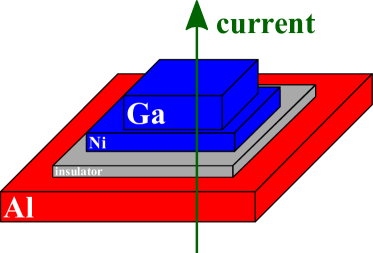
All investigated Al/Al2O3(/EuS)/Ni–Ga junctions—schematically illustrated in Fig. 1—with cross-section areas of were prepared by means of thermal evaporation inside an ultra-high vacuum (UHV) system with a base pressure of using in-situ shadow-masking techniques. During the growth process, thin layers of Al, Ni, Ga, and (partly) EuS were evaporated on clean glass substrates kept at temperatures of about . Ultrathin Al2O3 tunneling barriers, separating adjacent Al and (EuS/)Ni–Ga films, were created in situ either by exposing Al to a controlled oxygen plasma (producing Al2O3 barriers about thick) or deposited from an source using electron-beam evaporation (to obtain thinner Al2O3 barriers). Before taking the junctions out of the UHV chamber, they were protected by -thick Al2O3 layers.
In one run, we could prepare several junctions differing only in the thicknesses of individual Al, EuS, Ni, or Ga layers, while keeping all other growth parameters the same. To measure the tunneling conductance, and thus study the ramifications of the superconducting magnetic Ni–Ga bilayers on transport, we attached the junctions to a probe with electrical leads and immersed the system into a pumped liquid-helium bath (either or ) to reach a temperature of about or . Both Al and Ni–Ga thin films turned superconducting, with critical temperatures strongly dependent on their thickness. All our samples were based on -thick Al films (serving as the left electrode; please note that studying the tunneling conductance requires two distinct superconducting electrodes, which is in stark contrast to STM studies [71] that could probe the Ni–Ga bilayers alone), which have themselves already been intensively investigated in Al/EuS/Al junctions earlier [80] and demonstrated to remain superconducting below a critical temperature of about ; the superconducting coherence length of such thin Al films was estimated by Meservey and Tedrow [81] to be . Due to the strong competition between ferromagnetism and superconductivity, the critical temperature of the Ni–Ga bilayers (serving as the right electrode) is mostly determined by the thickness of the Ni film, and usually drops down with increasing Ni thickness (stronger ferromagnetic exchange). At about Ni, the critical temperature of the Ni–Ga bilayer is roughly ; typical superconducting coherence lengths of Ni ()–Ga () bilayers are of the order of [42]. Performing Meservey–Tedrow spectroscopy [82, 83, 81], we further estimated that the weak intrinsic ferromagnetic exchange within thin Ni films causes spin polarizations of about , which noticeably increase above Ni thickness.
| sample A | Al ()/Al2O3 ()/ |
|---|---|
| Ni ()–Ga ()/ () | |
| sample B | ()/ ()/ |
| ()– ()/ () | |
| sample C | ()/ ()/ |
| ()– ()/ () | |
| sample D | ()/ ()/ ()/ |
| ()– (/ () |
2.2 Tunneling-conductance measurements
To demonstrate the most puzzling transport features of Ni–Ga-bilayer junctions that we could detect in our series of experiments, we focus on four different samples (labeled sample A through sample D; see Tab. 1) containing either a thicker Ni ()–Ga () or a thinner ()– () bilayer, respectively. All tunneling-conductance data was obtained using standard lock-in technique.
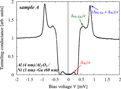
Sample A. First, we studied the Al ()/Al2O3 ()/Ni ()–Ga ()/ () junction with a thicker Ni ()–Ga () bilayer and at a temperature of about . The results of our measurements, which are shown in Fig. 2, reveal three distinct main (first-order) conductance maxima.
The quasiparticle tunneling conductance of similar (Josephson-like) junction geometries, consisting of two superconducting electrodes that are separated by a thin nonsuperconducting link, has already been intensively investigated in numerous systems and by several authors before (see, e.g., Refs. [84, 85, 86, 87, 88, 89, 90, 91, 92, 93, 94]). Rowell and Feldman [91, 93] developed thereby one of the perhaps most fundamental theoretical descriptions of these S/N/S’ junctions’ tunneling conductance, assuming two dissimilar superconducting electrodes S and S’ connected by a thin nonsuperconducting N link. Their Rowell–Feldman approach predicts the emergence of main conductance peaks whenever the applied bias voltage satisfies , , or , where () denotes the superconducting gap of S (S’) and refers to the positive elementary charge. At the microscopic level, Arnold [95, 96] related the appearance of these conductance peaks to multiple Andreev reflections that occur at these particular bias voltages.
Interestingly, we can directly adapt the predictions of the Rowell–Feldman model to understand the conductance features that we observed in sample A (see Fig. 2). We identify the thin Al film on the left- and the Ni–Ga bilayer on the right-hand side as the superconducting electrodes S and S’ of our samples, while the thin Al2O3 tunneling barrier serves as the nonsuperconducting link. From the main conductance peaks (maxima) displayed in Fig. 2, we can therefore estimate the superconducting gaps of Al, , and Ni–Ga, , such that the conductance maxima arise at , , and , accordingly. At a temperature of about , at which the conductance measurements were performed, we finally obtain —which is in good agreement with such thin Al films’ (zero-temperature) gap of about [42]—as well as ; the latter might be compared to the gap of an earlier studied Ni ()–Ga () bilayer [42], which was estimated to be about and is one of the rare references of Ni–Ga bilayers that are available in the literature. Since the Rowell–Feldmann approach suffices to satisfactorily explain the conductance features of sample A, and extract physically reasonable values of the Al and Ni–Ga-bilayer electrodes’ superconducting gaps, we might conclude already at this point that the ferromagnetic exchange inside Ni does not substantially affect the physics of the thicker Ni ()–Ga () bilayer; recall that Rowell and Feldman did not account for ferromagnetic components. We will in fact see later on that the interface magnetization of thicker Ni–Ga bilayers remains more uniform and, most likely due to their simultaneously weak spin polarizations of just about , the Ni films’ ferromagnetism does consequently not yet raise novel physics in thicker Ni ()–Ga () bilayers.
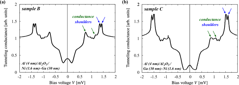
Samples B and C. The second and third samples that we investigated were composed of the ()/ ()/ ()– ()/ () junction with a thinner ()– () bilayer and the ()/ ()/ ()– ()/ () junction with an effectively “inverted” ()– () bilayer, respectively. The corresponding tunneling conductances measured at a temperature of about , which are shown in Fig. 3, reflect much richer conductance features than before (in sample A).
Specifically, each of the two large-bias (taking the gap of the thin Al film as the smallest energy reference in the system) conductance maxima that we associated with and in sample A seems to split into a subseries of (at least) two distinct and individually resolvable conductance maxima, which we will call conductance shoulders hereinafter. These conductance shoulders have not yet been explored in prior works; providing a sophisticated picture of their physical origin is therefore the main objective of our paper.
As the conductance shoulders only arise in junctions with thinner Ni–Ga bilayers, they are most likely intimately connected with novel physical phenomena that solely arise in thinner Ni–Ga bilayers. In our earlier theoretical work on the transport characteristics of ferromagnet/superconductor/ferromagnet junctions in the presence of interfacial spin-orbit interactions [97], we identified splittings of main conductance peaks into a shoulder-like pattern as signatures of “unconventional” (i.e., spin-flip) Andreev reflections at the interfaces. These unconventional Andreev reflections effectively induce superconducting triplet pairings in the junction. From that point of view, the large-bias conductance shoulders occurring in junctions with thinner ()– () bilayers might likewise provide transport fingerprints of superconducting triplet pairings. Nevertheless, before we can safely establish a connection between conductance shoulders and triplet superconductivity, we need to provide clear experimental evidence of the latter—which we will when analyzing the results of our polarized neutron reflectometry measurements.
Furthermore, the conductance data of samples B and C also reveal clearly visible zero-bias conductance peaks, which we did not detect in sample A with the thicker ()– () bilayer. Deducing the physical mechanism that causes such zero-bias peaks is usually a highly nontrivial task, as they could stem from numerous distinct phenomena—like, for example, zero-energy Andreev reflections [98, 99] or, as well in some cases, superconducting triplet pairings [100, 101]. More specifically, a previous experimental study [100] demonstrated that unexpectedly pronounced zero-bias conductance peaks (with amplitudes even exceeding those of their normal-state counterparts) arising in the tunneling conductance of superconductor/half-metal bilayers may be indicative of triplet superconductivity. At the microscopic level, inhomogeneous magnetizations around the interface can flip some of the Cooper-pair electrons’ spins, and thereby generate a “mixture” of spin-singlet and spin-triplet components in the superconducting order parameter [63, 46, 64, 65, 66, 67, 68, 50, 69, 51, 70, 100, 101, 102, 103, 71, 104].
In bilayers that contain not fully spin-polarized ferromagnets (i.e., no half metals as the second electrode), the situation might be much more intriguing. Thoroughly investigating electrical transport through Al/EuS bilayers, Diesch et al. [71] revealed that—instead of a single zero-bias conductance peak—superconducting triplet pairings give then rather rise to a rich, and not necessarily symmetric with respect to zero bias, low-bias double-peak conductance pattern, in which the gap between the two newly forming conductance peaks could be connected to the strength of the induced triplet pairings. Within the applied STM techniques, it was furthermore possible to individually address different transverse channels of the Al/EuS-bilayer junctions. As a result, Diesch and coworkers proposed that the magnetization around the Al/EuS interface is indeed inhomogeneous (on a length scale of a few nanometers, which could refer to the grain size of thin EuS films), which is again most likely the mechanism that is responsible for the aforementioned “mixing” of singlet and triplet order parameters.
Coming back to samples B and C of our study, we must therefore conclude that the appearance of zero-bias conductance peaks alone is neither a unique nor a sufficient signature of superconducting triplet pairings, and might as well originate from different physical effects. However, as the main focus of our work is to understand the peculiar large-bias conductance shoulders, and interpret these as clear fingerprints of triplet pairings, we did not further analyze the zero-bias peaks.
As another remarkable experimental feature, our conductance measurements on samples B and C suggest that replacing the ()– () by a ()– () bilayer—i.e., inverting the order of the Ni and Ga films inside the bilayers—has no substantial effect on the large-bias conductance shoulders [see Figs. 3(a) and 3(b)]. We take this finding as an experimental hint that the physics being responsible for the formation of large-bias conductance shoulders occurs around the Ni–Ga interface, and is thus quite independent of the order of the Ni and Ga films. Together with our claim that the conductance shoulders signify superconducting triplet pairings, we could therefore argue that the physical mechanism inducing triplet correlations in Ni–Ga bilayers could be similar to the aforementioned ones; i.e., the magnetization around the interface of ()– () bilayers is inhomogeneous (on a length scale of a few nanometers), which partially converts spin-singlet into spin-triplet Cooper pairs through flipping some of the electrons’ spins. Nonetheless, this interpretation certainly requires more pertinent experimental evidence, which we will provide within our polarized neutron reflectometry measurements that are directly able to probe the profile of the interface magnetizations and thereby support our predictions.
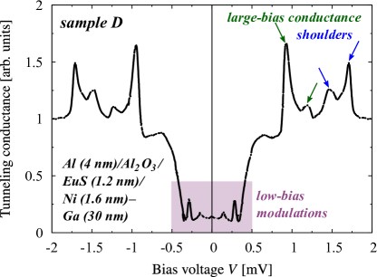
Sample D. As the thin Ni films of our junctions are only weakly ferromagnetic (recall that we deduced spin polarizations of about from Meservey–Tedrow spectroscopy)—and the triplet-pairing effects are thus most likely also rather moderate—, a more promising perspective could be to focus on samples that contain a second strongly ferromagnetic component. The fourth studied sample consisted therefore of the ()/ ()/ ()/ ()– (/ () junction, which basically corresponds to sample B except for the additional -thick barrier composed of the strong ferromagnetic insulator EuS [105, 106]. Such barriers have attracted considerable attention after earlier works [107, 80] had demonstrated that their high spin-filtering efficiency indeed provides an experimentally well-controllable way to convert more singlet into triplet Cooper pairs, and thereby generate (almost) completely spin-polarized triplet supercurrents.
The tunneling conductance of sample D at a temperature of about is presented in Fig. 4.
As the most important feature, we assert that the large-bias conductance shoulders—which we claimed to signify superconducting triplet pairings at the Ni–Ga interface—are robust and even slightly more pronounced than in samples B and C (i.e., the splittings between the shoulders’ conductance maxima are slightly larger). This observation could be carefully interpreted as a possible experimental hint that the additional ferromagnetic EuS spacer may indeed amplify the triplet pairings. Moreover, adding EuS gives rise to extremely rich low-bias conductance modulations that we could not detect in samples A through C in which EuS was absent. As we pointed out previously, STM studies of Al/EuS bilayers performed by Diesch et al. [71] indicated that low-bias conductance double peaks (rather than just a single zero-bias conductance peak) could provide another signature of interfacial triplet pairings. Our results obtained from sample D look physically similar, apart from detecting four instead of two low-bias peaks (two at negative and two at positive voltages, respectively). Analogously to the zero-bias peaks of samples B and C, unraveling the physical origin of these low-bias features has not yet been possible with the available data, and goes also beyond the scope of this manuscript. One possible explanation for the doubling of low-bias peaks (when compared to Diesch’s work) might be that we are dealing with two different ferromagnetic films—EuS and Ni—instead of just one (EuS) as Diesch and coworkers, and thus need to consider two distinct interfaces at which the magnetization may be inhomogeneous. However, this is a premature statement that we cannot uniquely confirm from our measurements.
2.3 Polarized neutron reflectometry
While discussing the tunneling-conductance data obtained from samples B and C in the preceding section, we argued that the observed large-bias conductance shoulders might serve as an experimentally accessible transport signature of superconducting triplet pairings getting induced by inhomogeneous magnetizations around the interface of thinner ()– ( bilayers. In the following, we wish to provide independent experimental evidence of this claim through a deeper characterization of the physical properties of this peculiar interface.
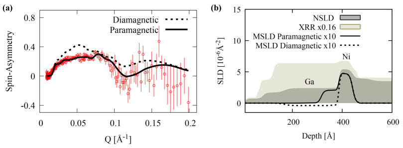
For a deeper investigation of the Ni–Ga interface, and to directly explore its structure and magnetization depth profile, we combine depth-sensitive polarized neutron reflectometry (PNR) with low-angle x-ray reflectometry (XRR) studies. Being electrically neutral, spin-polarized neutrons penetrate the entire multilayer junctions, probing the magnetic and structural composition of their films through buried interfaces down to the substrate [108]. PNR allows for a direct determination of both the absolute value and the direction of the magnetic field induced inside the superconductor and was previously successfully applied to observe the diamagnetic Meissner effect, as well as vortex-line distributions, in niobium- and YBCO-bilayer films [109, 110]. In this paper, we report on the detection of inhomogeneous interface magnetizations and the paramagnetic Meissner effect in superconducting Ga, which altogether confirm our earlier claims that the proximity coupling in the Ni–Ga bilayer indeed induces superconducting triplet states [76, 53, 77, 78, 79, 111] near the interface, appearing to be responsible for the experimentally observed large-bias conductance shoulders. The PNR experiments were performed on the Magnetism Reflectometer at the Spallation Neutron Source at Oak Ridge National Laboratory [109, 112], using a neutron beam with a wavelength band of – and high polarization of to . After cooling in zero field (ZFC), measurements were conducted at temperatures of and , with an external magnetic field applied in the plane of the sample up to . Using the time-of-flight method, a collimated polychromatic beam of polarized neutrons with a wavelength band impinges on the film at a grazing incidence angle , where it interacts with atomic nuclei and the spins of unpaired electrons. Then, the reflected intensity is measured as a function of the wave-vector transfer for two neutron polarizations and with the neutron spin parallel () or antiparallel () to the direction of the external field ; denotes the neutron wavelength. To separate nuclear from magnetic scattering, we present our data in terms of the spin-asymmetry ratio . For example, a value of means that there is no magnetic moment in the system. The depth profiles of the nuclear and magnetic scattering length densities (NSLD and MSLD) correspond to the depth profiles of the chemical and in-plane magnetization vector distributions, respectively. The total magnetization can be calculated from the MSLD data using the relation .
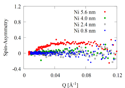
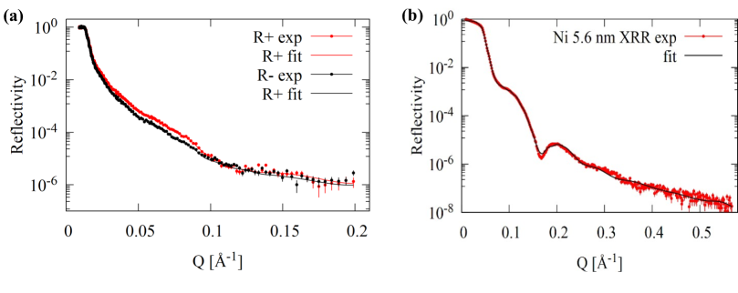
To verify the depth morphology of the films, we used complementary XRR data. These experiments were carried out on Ni–Ga bilayers with the Ga thickness fixed at about (fitting our data, we obtain Ga thickness), while the Ni thickness was varied to cover , , , and ; see Fig. 5. These bilayers are comparable (in film thicknesses) to those in samples B and C, which let the puzzling large-bias conductance shoulders occur. We explored the behavior of the magnetization of the bilayers above and below their critical temperature. The samples were investigated under the same conditions as above, starting with ZFC down to and measuring at . After that, the magnetic field was turned off, the sample was cooled to , and the measurement was repeated at a magnetic field of . The sample with the -thick Ni film showed a clear magnetic signal [i.e., clear SA splitting between reflectivity for neutrons with spin up () and spin down ()]. For the sample containing the -thick Ni film, the SA magnetic signal was reduced by a factor of 3, while no measurable magnetization could be detected (within the accuracy of this method) for the samples with the - and -thick Ni films. NSLD and MSLD depth profiles were obtained by simultaneous fitting to PNR and XRR data (shown in Fig. 6), and finally plotted as a function of depth from the surface (see Fig. 7) for the sample with the -thick Ni film.
To analyze the electromagnetic proximity effect in Ni–Ga-bilayer structures from the PNR data, we distinguish between two scenarios: (1) the conventional diamagnetic Meissner screening and (2) the paramagnetic Meissner response in Ga. The results for both cases are shown in Fig. 7. Fitting the PNR (obtained at , which is below that bilayer’s superconducting critical temperature) and XRR data, we observe that the Ni ()–Ga () interface is sharp with a roughness of . The thickness of the Ga layer refined by the fit is . The PNR spin-asymmetry ratio reveals that the best fit to the data requires induced magnetization over roughly in Ga in the vicinity of the Ni–Ga interface, while the magnetization in the Ni film is about and uniform. For comparison and confirmation of our findings, we additionally consider the model of diamagnetic Meissner screening with a penetrating flux. In this case, the MSLD profile will have a contribution from the magnetic field penetration depth from both interfaces of the film. Given that the Ga layer is only thick, the magnetic field penetrates the entire film [113] so that the diamagnetic effect is significantly reduced [see dashed line in Fig. 7(b)] and the corresponding SA in Fig. 7(a) shows considerable deviations from the experimental points. We are thus able to directly see the induced ferromagnetic order’s influence inside the Ga layer right at the interface with the Ni film, which should be attributed to the paramagnetic Meissner response. Therefore, PNR provides strong independent experimental evidence [76, 53, 77, 78, 79] of our claims that inhomogeneous magnetizations induce superconducting triplet pairings near the interface of the Ni–Ga bilayer.
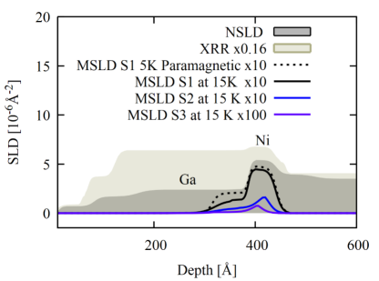
To better illustrate the impact of the thickness of the Ni film on the interface and magnetization structure, we analyze the PNR data obtained from Ni–Ga bilayers with , , and Ni films (recall Fig. 5) in a similar manner; the thickness of Ga is still . From these data analyses, presented in Fig. 8, we could indeed detect a significant difference between the structural (nonmagnetic) and the magnetic Ni–Ga interface roughness. While the structural interfacial roughness is about for -thick Ni, we extract roughness for -, -, and -thick Ni, respectively. From the PNR measurements performed at magnetic field and temperature, we deduce that the interfacial magnetization is inhomogeneous and extending over several nanometers of , , and (for -thick, -thick, and -thick Ni). For the bilayer containing Ni, the accuracy of our approach does not suffice to resolve the magnetization profile. As a more inhomogeneous interface magnetization is expected to convert more spin-singlet into spin-triplet Cooper pairs to enhance the triplet-pairing mechanism, it could thus be promising to explore as a next step the tunneling conductance of bilayers altering the thickness of the Ni film (and keeping Ga the same). Increasing the Ni thickness might then suppress and decreasing the Ni thickness further amplify the triplet pairings, and therefore the conductance shoulders shall become either less or more pronounced.
3 Theoretical toy model: Large-bias conductance shoulders as signatures of interfacial triplet pairings
As we outlined in Sec. 2 when discussing our experimental results, the appearance of large-bias shoulders in the tunneling conductance of Ni–Ga bilayers can serve as a signature of superconducting triplet pairings induced at the Ni–Ga interface—microscopically originating from inhomogeneous interface magnetizations, as our PNR analyses clearly demonstrated. In this final section of our paper, we formulate a purely phenomenological toy model to theoretically convince at the qualitative level that superconducting triplet pairings at the Ni–Ga interface give indeed rise to the experimentally detected large-bias conductance shoulders.
3.1 Phenomenological toy model
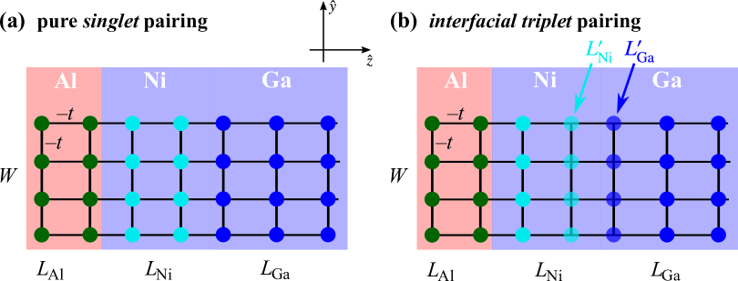
To describe quasiparticle excitations in Al/Ni–Ga junctions (for simplicity, our toy model neglects the Al2O3 tunneling barriers), we formulate their Bogoliubov–de Gennes Hamiltonian [114] on a lattice and compute the tunneling DOS at zero temperature using the Python transport package Kwant [115]. For simplicity, we consider a two-dimensional square lattice with spacing between two adjacent lattice sites; each site with the real-space coordinates is uniquely identified by its integer lattice indices . Figure 9(a) shows a graphical representation of the chosen tight-binding lattice. We denote the numbers of lattice sites along the longitudinal -direction inside the Al, Ni, and Ga junction regions by , , and , respectively, whereas we assume in total lattice sites along the transverse -direction.
The on-site energies (with respect to the Fermi level) at lattice site are then given by the discretized Nambu-space Bogoliubov–de Gennes Hamiltonian [ denotes the Heaviside step function]
| (1) |
and the nearest-neighbor hoppings ( indicates nearest-neighbor lattice sites) by
| (2) |
where
| (3) |
Thereby, the hopping parameter represents , where refers to the effective quasiparticle masses. For our mostly to a qualitative level restricted modeling, it is most convenient to use such units that .
Apart from the discrete single-particle energies and the ferromagnetic exchange gap of Ni (the magnetization vector points along the -direction), we need to account for the films’ distinct superconducting gaps. The Bogoliubov–de Gennes Hamiltonian involves now not only singlet superconducting gaps (pairing potentials), coupling spin-up and spin-down electrons to form spin-singlet Cooper pairs, but also triplet gaps (pairing potentials) that facilitate spin-triplet Cooper pairs consisting of two equal-spin electrons. While the singlet superconducting gaps are abbreviated by and , the triplet gap is denoted by . To ensure that triplet correlations really only occur in the vicinity of the Ni–Ga interface, their respective pairing-potential terms are nonzero only in and of Ni’s and Ga’s lattice sites around the Ni–Ga interface, as we schematically illustrate in Fig. 9(b).
Since the inhomogeneous magnetization at the Ni–Ga interfaces, which ultimately induces the triplet pairings we are interested in, stems from a highly complex inhomogeneous magnetic domain structure that has not yet been fully understood at the microscopic level, we manually introduce the interfacial triplet pairings into our toy model through including nonzero tunable equal-spin superconducting pairing terms around the Ni–Ga interface. While this is sufficient to unravel the physical origin of the observed conductance shoulders, more comprehensive, and at the same time more realistic from a microscopic point of view, modeling is certainly desirable at a later stage, after gaining more experimental insight into the magnetic texture at the interface and possibly assisted by first-principles band-structure calculations [116, 117, 118].
To proceed, we implement the tight-binding Bogoliubov–de Gennes Hamiltonian, given by Eq. (1), in Kwant, and use Kwant’s internal Kernel Polynomial Method (KPM) to extract the junctions’ spatially integrated zero-temperature tunneling DOS (normalized to its normal-state counterpart) that we essentially probe through our conductance measurements. Along the transverse direction, we include lattice sites. Although changing does not qualitatively impact the tunneling DOS (for that reason, we could also completely neglect the third spatial orientation, i.e., the -direction, in our junctions), using rather large numbers is reasonable to minimize numerical errors, which might cause unphysical numerical fluctuations in the DOS data.
3.2 Tunneling-DOS simulations and large-bias conductance shoulders
Figure 10 illustrates the computed tunneling DOS of the Al/Ni–Ga junction with the lattice-site numbers , , and ; note that these were chosen such that their ratio matches the film-thickness ratio of sample B, although one cannot directly compare the theoretical and experimental dimensions as we chose as the lattice constant in our Kwant simulations. The specific values substituted for the singlet superconducting gaps of the Al film and the Ni–Ga bilayer are not particularly relevant to the results; we kept them at and in order to scale their ratio roughly according to the experimentally from sample A extracted gaps. The amplitude of the superconducting triplet gap, which is only present in the vicinity of the Ni–Ga interface, was initially increased from (no triplet pairing) to (moderate triplet pairing), and finally to (strong triplet pairing). Enhancing the triplet-pairing strength in our model corresponds to produce a more inhomogeneously magnetized interface domain texture in the experiment, which is expected to occur—coinciding with our experimental results—when decreasing the Ni(–Ga bilayer) thickness to get a rougher interface.
Despite the particular values of triplet gaps substituted into our calculations may seem exaggeratedly large when compared to their singlet counterparts, we can still use them in our numerical simulations to develop a qualitative understanding of the underlying physics. One of the reasons that such large triplet gaps are required to reproduce the experimental findings could be the fact that we did not take care of formulating the full model using physically realistic units (recall that we set, for instance, . Furthermore, and as we mentioned earlier, the triplet-pairing mechanisms in the real samples are a consequence of complex nonuniform interface magnetizations and are therefore at the microscopic level much more complicated to properly describe than in our strongly simplified phenomenological model. The “effectiveness” of induced triplet pairings depends additionally also on the strength of ferromagnetism inside the magnetic junction films. We assumed an extremely small exchange energy gap in Ni of —when compared to the singlet superconducting gaps, which are typically orders of magnitude smaller than ferromagnetic exchange couplings—in our simulations to demonstrate that even extremely weak ferromagnetism suffices to observe transport ramifications of superconducting triplet pairings. Considering a typical metal Fermi level , corresponds to a Ni spin polarization of just . Although Meservey–Tedrow spectroscopy indicated that the Ni spin polarization in our samples is only about , this is still notably larger than the tiny value assumed for our simulations, which could provide another reason for the large effective triplet pairings required in our simulations to recover the experimentally evident features.
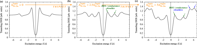
In the absence of triplet pairing at the Ni–Ga interface, we recover two DOS maxima (becoming visible in our transport measurements in terms of conductance maxima) that we associated with the energies of the singlet superconducting gaps of Al and the Ni–Ga bilayer when analyzing the experimental data obtained from sample A (recall the Rowell-Feldman description explained in Sec. 2). Already moderate triplet pairing, however, turns the first DOS maximum at the lower of the two bias voltages into two neighboring maxima, and thereby forms the first shoulder that we probably witnessed in the conductance spectrum of sample B. The second experimentally observed shoulder at slightly larger bias voltage eventually appears when the triplet-pairing strength is further enhanced. The latter shoulder (i.e., the one at larger bias voltage) seems to be less sensitive to interfacial triplet pairings in general since the splitting between its two neighboring conductance maxima is substantially smaller than that within the first—in good agreement with our experimental results (recall the conductance data of samples B and C presented in Fig. 3)—and requires thus a more sizable triplet-pairing strength to become indeed evident. Although our theoretical DOS simulations are robust enough to qualitatively demonstrate that the experimentally detected large-bias conductance shoulders indeed provide a transport fingerprint of triplet pairings at the Ni–Ga bilayer interface, theory and experiment can, at least at this point, not be compared to each other at the quantitative level due to the strong simplifications made in our model.
4 Conclusions
In summary, we thoroughly discussed and analyzed our tunneling-conductance measurements on superconducting magnetic Al/(/EuS)/Ni–Ga junctions, focusing, in particular, on thicker Ni ()–Ga () and thinner ()– () bilayers, respectively. While the conductance spectrum in the first case could be explained based on the findings of earlier studies, the second scenario turned out to become much more puzzling, as it mainly led to the additional formation of unexpected large-bias conductance shoulders that have not yet been understood. Since the latter remained mostly unaffected when “inverting” the Ni and Ga films, we concluded that all important physics should happen near the Ni–Ga interface.
Performing PNR analyses to collect more information about the structure and magnetization of this interface, we detected the paramagnetic Meissner response in Ga to convince that the proximity-coupled bilayer induces superconducting triplet pairings around the Ni–Ga interface. With this in mind, we elaborated on a strongly simplified theoretical toy model, which allowed us to compute the junctions’ tunneling DOS that our conductance measurements essentially probe. Comparing our phenomenological DOS simulations with experimental conductance data substantiated that the conductance shoulders do indeed provide a well-accessible transport fingerprint of newly induced superconducting triplet correlations in the vicinity of the Ni–Ga interface.
To further characterize the novel triplet pairings within the Ni–Ga bilayer, we suggest to subsequently analyze the Ni–Ga-interface profile through SQUID and Lorentz-microscopy measurements, which can directly probe inhomogeneous spin textures around the interface. Moreover, investigating our samples’ transport characteristics in the presence of an external magnetic field might give deeper insight into the triplet-pairing mechanism, as this manipulates the inhomogeneity of the interface magnetizations and shall therefore give a unique magnetization dependence to the conductance shoulders.
References
References
- [1] Žutić I, Fabian J and Das Sarma S 2004 Rev. Mod. Phys. 76 323–410 URL http://link.aps.org/doi/10.1103/RevModPhys.76.323
- [2] Fabian J, Matos-Abiague A, Ertler C, Stano P and Žutić I 2007 Acta Phys. Slovaca 57 565–907 URL http://www.physics.sk/aps/pub.php?y=2007&pub=aps-07-04
- [3] Eschrig M 2011 Phys. Today 64 43–49 URL http://scitation.aip.org/content/aip/magazine/physicstoday/article/64/1/10.1063/1.3541944
- [4] Linder J and Robinson J W A 2015 Sci. Rep. 5 15483 ISSN 2045-2322 URL http://dx.doi.org/10.1038/srep15483http://www.nature.com/articles/srep15483
- [5] Ohnishi K, Komori S, Yang G, Jeon K R, Olde Olthof L A B, Montiel X, Blamire M G and Robinson J W A 2020 Appl. Phys. Lett. 116 130501 ISSN 0003-6951 URL http://aip.scitation.org/doi/10.1063/1.5138905
- [6] Ioffe L B, Geshkenbein V B, Feigel’man M V, Fauchère A L and Blatter G 1999 Nature 398 679–681 URL http://www.nature.com/nature/journal/v398/n6729/abs/398679a0.html
- [7] Mooij J E, Orlando T P, Levitov L, Tian L, van der Wal C H and Lloyd S 1999 Science 285 1036–1039 URL http://science.sciencemag.org/content/285/5430/1036
- [8] Blatter G, Geshkenbein V B and Ioffe L B 2001 Phys. Rev. B 63 174511 ISSN 0163-1829 URL https://link.aps.org/doi/10.1103/PhysRevB.63.174511
- [9] Ustinov A V and Kaplunenko V K 2003 J. Appl. Phys. 94 5405 ISSN 00218979 URL http://scitation.aip.org/content/aip/journal/jap/94/8/10.1063/1.1604964
- [10] Yamashita T, Tanikawa K, Takahashi S and Maekawa S 2005 Phys. Rev. Lett. 95 097001 URL http://link.aps.org/doi/10.1103/PhysRevLett.95.097001
- [11] Feofanov A K, Oboznov V A, Bol’ginov V V, Lisenfeld J, Poletto S, Ryazanov V V, Rossolenko A N, Khabipov M, Balashov D, Zorin A B, Dmitriev P N, Koshelets V P and Ustinov A V 2010 Nat. Phys. 6 593–597 URL http://www.nature.com/doifinder/10.1038/nphys1700
- [12] Khabipov M I, Balashov D V, Maibaum F, Zorin A B, Oboznov V A, Bolginov V V, Rossolenko A N and Ryazanov V V 2010 Supercond. Sci. Technol. 23 045032 ISSN 0953-2048 URL https://iopscience.iop.org/article/10.1088/0953-2048/23/4/045032
- [13] Devoret M H and Schoelkopf R J 2013 Science 339 1169–1174 URL http://science.sciencemag.org/content/339/6124/1169
- [14] Soulen Jr R J 1998 Science 282 85–88 ISSN 00368075 URL https://www.sciencemag.org/lookup/doi/10.1126/science.282.5386.85
- [15] Soulen Jr R J, Osofsky M S, Nadgorny B, Ambrose T, Broussard P, Cheng S F, Byers J, Tanaka C T, Nowack J, Moodera J S, Laprade G, Barry A and Coey M D 1999 J. Appl. Phys. 85 4589–4591 ISSN 00218979 URL http://scitation.aip.org/content/aip/journal/jap/85/8/10.1063/1.370417
- [16] de Jong M J M and Beenakker C W J 1995 Phys. Rev. Lett. 74 1657–1660 URL http://link.aps.org/doi/10.1103/PhysRevLett.74.1657
- [17] Golubov A A, Kupriyanov M Y and Il’ichev E 2004 Rev. Mod. Phys. 76 411–469 URL http://link.aps.org/doi/10.1103/RevModPhys.76.411
- [18] Yu L 1965 Acta Phys. Sin. 21 75–91 URL http://wulixb.iphy.ac.cn/CN/Y1965/V21/I1/75
- [19] Shiba H 1968 Prog. Theor. Phys. 40 435–451 URL https://academic.oup.com/ptp/article/40/3/435/1831894/Classical-Spins-in-Superconductors
- [20] Rusinov A I 1968 Zh. Eksp. Teor. Fiz. Pisma Red. 9 146
- [21] Rusinov A I 1969 JETP Lett. 9 85 URL http://www.jetpletters.ac.ru/ps/1658/article_25295.shtml
- [22] Costa A, Fabian J and Kochan D 2018 Phys. Rev. B 98 134511 ISSN 2469-9950 URL http://arxiv.org/abs/1803.02063https://link.aps.org/doi/10.1103/PhysRevB.98.134511
- [23] Kochan D, Barth M, Costa A, Richter K and Fabian J 2020 Phys. Rev. Lett. 125 087001 ISSN 1079-7114 URL https://doi.org/10.1103/PhysRevLett.125.087001
- [24] Bulaevskii L N, Kuzii V V and Sobyanin A A 1977 Pis’ma Zh. Eksp. Teor. Fiz. 25 314–318
- [25] Bulaevskii L N, Kuzii V V and Sobyanin A A 1977 JETP Lett. 25 290–294 URL http://www.jetpletters.ac.ru/ps/1410/article_21163.shtml
- [26] Ryazanov V V, Oboznov V A, Rusanov A Y, Veretennikov A V, Golubov A A and Aarts J 2001 Phys. Rev. Lett. 86 2427–2430 URL http://link.aps.org/doi/10.1103/PhysRevLett.86.2427
- [27] Nilsson J, Akhmerov A R and Beenakker C W J 2008 Phys. Rev. Lett. 101 120403 ISSN 0031-9007 URL https://link.aps.org/doi/10.1103/PhysRevLett.101.120403
- [28] Duckheim M and Brouwer P W 2011 Phys. Rev. B 83 054513 URL http://link.aps.org/doi/10.1103/PhysRevB.83.054513
- [29] Lee S P, Alicea J and Refael G 2012 Phys. Rev. Lett. 109 126403 ISSN 0031-9007 URL https://link.aps.org/doi/10.1103/PhysRevLett.109.126403
- [30] Nadj-Perge S, Drozdov I K, Li J, Chen H, Jeon S, Seo J, MacDonald A H, Bernevig B A and Yazdani A 2014 Science 346 602–607 URL http://www.sciencemag.org/content/346/6209/602.abstract
- [31] Dumitrescu E, Roberts B, Tewari S, Sau J D and Das Sarma S 2015 Phys. Rev. B 91 094505 ISSN 1098-0121 URL https://link.aps.org/doi/10.1103/PhysRevB.91.094505
- [32] Pawlak R, Kisiel M, Klinovaja J, Meier T, Kawai S, Glatzel T, Loss D and Meyer E 2016 npj Quantum Inf. 2 16035 ISSN 2056-6387 URL http://www.nature.com/articles/npjqi201635
- [33] Ruby M, Heinrich B W, Peng Y, von Oppen F and Franke K J 2017 Nano Lett. 17 4473–4477 ISSN 1530-6984 URL http://pubs.acs.org/doi/10.1021/acs.nanolett.7b01728
- [34] Livanas G, Sigrist M and Varelogiannis G 2019 Sci. Rep. 9 6259 ISSN 2045-2322 URL http://www.nature.com/articles/s41598-019-42558-3
- [35] Manna S, Wei P, Xie Y, Law K T, Lee P A and Moodera J S 2020 Proc. Natl. Acad. Sci. 117 8775–8782 ISSN 0027-8424 URL http://www.pnas.org/lookup/doi/10.1073/pnas.1919753117
- [36] Högl P, Matos-Abiague A, Žutić I and Fabian J 2015 Phys. Rev. Lett. 115 116601 URL http://journals.aps.org/prl/abstract/10.1103/PhysRevLett.115.116601
- [37] Högl P, Matos-Abiague A, Žutić I and Fabian J 2015 Phys. Rev. Lett. 115 159902(E) URL https://link.aps.org/doi/10.1103/PhysRevLett.115.159902
- [38] Jacobsen S H, Kulagina I and Linder J 2016 Sci. Rep. 6 23926 ISSN 2045-2322 URL http://www.nature.com/articles/srep23926
- [39] Costa A, Högl P and Fabian J 2017 Phys. Rev. B 95(2) 024514 URL https://link.aps.org/doi/10.1103/PhysRevB.95.024514
- [40] Martínez I, Högl P, González-Ruano C, Cascales J P, Tiusan C, Lu Y, Hehn M, Matos-Abiague A, Fabian J, Žutić I and Aliev F G 2020 Phys. Rev. Appl. 13 014030 ISSN 2331-7019 URL https://link.aps.org/doi/10.1103/PhysRevApplied.13.014030
- [41] Keizer R S, Goennenwein S T B, Klapwijk T M, Miao G, Xiao G and Gupta A 2006 Nature 439 825–827 URL http://www.nature.com/doifinder/10.1038/nature04499
- [42] Moodera J S and Meservey R 1990 Phys. Rev. B 42 179–183 ISSN 0163-1829 URL https://link.aps.org/doi/10.1103/PhysRevB.42.179
- [43] LeClair P, Moodera J S, Philip J and Heiman D 2005 Phys. Rev. Lett. 94 037006 ISSN 0031-9007 URL http://link.aps.org/doi/10.1103/PhysRevLett.94.037006https://link.aps.org/doi/10.1103/PhysRevLett.94.037006
- [44] Belzig W, Bruder C and Schön G 1996 Phys. Rev. B 53 5727–5733 ISSN 0163-1829 URL https://link.aps.org/doi/10.1103/PhysRevB.53.5727
- [45] Kadigrobov A, Shekhter R I and Jonson M 2001 Europhys. Lett. 54 394–400 ISSN 0295-5075 URL https://iopscience.iop.org/article/10.1209/epl/i2001-00107-2
- [46] Bergeret F S, Volkov A F and Efetov K B 2001 Phys. Rev. Lett. 86 4096–4099 URL http://link.aps.org/doi/10.1103/PhysRevLett.86.4096
- [47] Bergeret F S, Volkov A F and Efetov K B 2005 Rev. Mod. Phys. 77 1321–1373 URL http://link.aps.org/doi/10.1103/RevModPhys.77.1321
- [48] Yokoyama T, Tanaka Y and Golubov A A 2007 Phys. Rev. B 75 134510 ISSN 1098-0121 URL https://link.aps.org/doi/10.1103/PhysRevB.75.134510
- [49] Linder J, Yokoyama T, Sudbø A and Eschrig M 2009 Phys. Rev. Lett. 102 107008 ISSN 0031-9007 URL https://link.aps.org/doi/10.1103/PhysRevLett.102.107008
- [50] Khaire T S, Khasawneh M A, Pratt Jr W P and Birge N O 2010 Phys. Rev. Lett. 104 137002 URL https://link.aps.org/doi/10.1103/PhysRevLett.104.137002
- [51] Robinson J W A, Witt J D S and Blamire M G 2010 Science 329 59–61 ISSN 0036-8075 URL http://science.sciencemag.org/content/329/5987/59
- [52] Anwar M S, Czeschka F, Hesselberth M, Porcu M and Aarts J 2010 Phys. Rev. B 82 100501(R) ISSN 1098-0121 URL https://link.aps.org/doi/10.1103/PhysRevB.82.100501
- [53] Yokoyama T, Tanaka Y and Nagaosa N 2011 Phys. Rev. Lett. 106 246601 ISSN 0031-9007 URL https://link.aps.org/doi/10.1103/PhysRevLett.106.246601
- [54] Bergeret F S, Verso A and Volkov A F 2012 Phys. Rev. B 86 060506(R) ISSN 1098-0121 URL https://link.aps.org/doi/10.1103/PhysRevB.86.060506
- [55] Bergeret F S and Tokatly I V 2013 Phys. Rev. Lett. 110 117003 URL http://link.aps.org/doi/10.1103/PhysRevLett.110.117003
- [56] Bergeret F S and Tokatly I V 2014 Phys. Rev. B 89 134517 URL http://link.aps.org/doi/10.1103/PhysRevB.89.134517
- [57] Alidoust M, Halterman K and Valls O T 2015 Phys. Rev. B 92 014508 ISSN 1098-0121 URL https://link.aps.org/doi/10.1103/PhysRevB.92.014508
- [58] Di Bernardo A, Diesch S, Gu Y, Linder J, Divitini G, Ducati C, Scheer E, Blamire M G and Robinson J W A 2015 Nat. Commun. 6 8053 ISSN 2041-1723 URL http://www.nature.com/articles/ncomms9053
- [59] Arjoranta J and Heikkilä T T 2016 Phys. Rev. B 93 024522 ISSN 2469-9950 URL https://link.aps.org/doi/10.1103/PhysRevB.93.024522
- [60] Espedal C, Yokoyama T and Linder J 2016 Phys. Rev. Lett. 116 127002 ISSN 0031-9007 URL https://link.aps.org/doi/10.1103/PhysRevLett.116.127002
- [61] Pal A, Ouassou J A, Eschrig M, Linder J and Blamire M G 2017 Sci. Rep. 7 3–7 ISSN 20452322 URL http://dx.doi.org/10.1038/srep40604
- [62] Bergeret F S and Tokatly I V 2020 Phys. Rev. B 102 060506(R) ISSN 2469-9950 URL https://link.aps.org/doi/10.1103/PhysRevB.102.060506
- [63] Bergeret F S, Volkov A F and Efetov K B 2001 Phys. Rev. Lett. 86 3140–3143 ISSN 0031-9007 URL https://link.aps.org/doi/10.1103/PhysRevLett.86.3140
- [64] Bergeret F S, Volkov A F and Efetov K B 2001 Phys. Rev. B 64 134506 URL http://link.aps.org/doi/10.1103/PhysRevB.64.134506
- [65] Eschrig M, Kopu J, Cuevas J C and Schön G 2003 Phys. Rev. Lett. 90 137003 ISSN 0031-9007 URL https://link.aps.org/doi/10.1103/PhysRevLett.90.137003
- [66] Houzet M and Buzdin A I 2007 Phys. Rev. B 76 060504(R) ISSN 1098-0121 URL https://link.aps.org/doi/10.1103/PhysRevB.76.060504
- [67] Eschrig M and Löfwander T 2008 Nat. Phys. 4 138–143 URL http://dx.doi.org/10.1038/nphys831
- [68] Grein R, Eschrig M, Metalidis G and Schön G 2009 Phys. Rev. Lett. 102 227005 ISSN 0031-9007 URL https://link.aps.org/doi/10.1103/PhysRevLett.102.227005
- [69] Robinson J W A, Halász G B, Buzdin A I and Blamire M G 2010 Phys. Rev. Lett. 104 207001 URL https://link.aps.org/doi/10.1103/PhysRevLett.104.207001
- [70] Banerjee N, Robinson J W A and Blamire M G 2014 Nat. Commun. 5 1–6 ISSN 20411723
- [71] Diesch S, Machon P, Wolz M, Sürgers C, Beckmann D, Belzig W and Scheer E 2018 Nat. Commun. 9 5248 ISSN 2041-1723 URL http://www.nature.com/articles/s41467-018-07597-w
- [72] Satchell N and Birge N O 2018 Phys. Rev. B 97 214509 ISSN 2469-9950 URL https://link.aps.org/doi/10.1103/PhysRevB.97.214509
- [73] Satchell N, Loloee R and Birge N O 2019 Phys. Rev. B 99 174519 ISSN 2469-9950 URL https://link.aps.org/doi/10.1103/PhysRevB.99.174519
- [74] Eskilt J R, Amundsen M, Banerjee N and Linder J 2019 Phys. Rev. B 100 224519 ISSN 2469-9950 URL https://link.aps.org/doi/10.1103/PhysRevB.100.224519
- [75] Bujnowski B, Biele R and Bergeret F S 2019 Phys. Rev. B 100 224518 ISSN 2469-9950 URL https://link.aps.org/doi/10.1103/PhysRevB.100.224518
- [76] Machida K and Klemm R A 1978 Solid State Commun. 27 1061–1063 ISSN 00381098 URL https://linkinghub.elsevier.com/retrieve/pii/0038109878911109
- [77] Alidoust M, Halterman K and Linder J 2014 Phys. Rev. B 89 054508 ISSN 1098-0121 URL https://link.aps.org/doi/10.1103/PhysRevB.89.054508
- [78] Asano Y, Fominov Y V and Tanaka Y 2014 Phys. Rev. B 90 094512 ISSN 1098-0121 URL https://link.aps.org/doi/10.1103/PhysRevB.90.094512
- [79] Di Bernardo A, Salman Z, Wang X L, Amado M, Egilmez M, Flokstra M G, Suter A, Lee S L, Zhao J H, Prokscha T, Morenzoni E, Blamire M G, Linder J and Robinson J W A 2015 Phys. Rev. X 5 041021 ISSN 2160-3308 URL https://link.aps.org/doi/10.1103/PhysRevX.5.041021
- [80] Rouco M, Chakraborty S, Aikebaier F, Golovach V N, Strambini E, Moodera J S, Giazotto F, Heikkilä T T and Bergeret F S 2019 Phys. Rev. B 100 184501 ISSN 2469-9950 URL https://doi.org/10.1103/PhysRevB.100.184501https://link.aps.org/doi/10.1103/PhysRevB.100.184501
- [81] Meservey R and Tedrow P M 1994 Phys. Rep. 238 173–243 URL https://doi.org/10.1016/0370-1573(94)90105-8
- [82] Tedrow P M and Meservey R 1971 Phys. Rev. Lett. 26 192–195 ISSN 00319007
- [83] Tedrow P M and Meservey R 1973 Phys. Rev. B 7 318–326 ISSN 01631829
- [84] Taylor B N and Burstein E 1963 Phys. Rev. Lett. 10 14–17 ISSN 0031-9007 URL https://link.aps.org/doi/10.1103/PhysRevLett.10.14
- [85] Adkins C J 1963 Philos. Mag. 8 1051–1061 ISSN 0031-8086 URL http://www.tandfonline.com/doi/abs/10.1080/14786436308214463
- [86] Adkins C J 1964 Rev. Mod. Phys. 36 211–213 ISSN 0034-6861 URL https://link.aps.org/doi/10.1103/RevModPhys.36.211
- [87] van Huffelen W M, Klapwijk T M, Heslinga D R, de Boer M J and van der Post N 1993 Phys. Rev. B 47 5170–5189 ISSN 0163-1829 URL https://link.aps.org/doi/10.1103/PhysRevB.47.5170
- [88] Kuhlmann M, Zimmermann U, Dikin D, Abens S, Keck K and Dmitriev V M 1994 Z. Phys. B 96 13–24 ISSN 0722-3277 URL http://link.springer.com/10.1007/BF01313010
- [89] Zimmermann U, Abens S, Dikin D, Keck K and Dmitriev V M 1995 Z. Phys. B 97 59–66 ISSN 0722-3277 URL https://linkinghub.elsevier.com/retrieve/pii/0921453494921733http://link.springer.com/10.1007/BF01317588
- [90] Rowell J M 1964 Rev. Mod. Phys. 36 199–200 ISSN 0034-6861 URL https://link.aps.org/doi/10.1103/RevModPhys.36.199
- [91] Rowell J M and Feldmann W L 1968 Phys. Rev. 172 393–401 ISSN 0031-899X URL https://link.aps.org/doi/10.1103/PhysRev.172.393
- [92] Klapwijk T M, Blonder G E and Tinkham M 1982 Physica 109 & 110B 1657–1664 URL https://doi.org/10.1016/0378-4363(82)90189-9
- [93] Octavio M, Tinkham M, Blonder G E and Klapwijk T M 1983 Phys. Rev. B 27 6739–6746 ISSN 0163-1829 URL https://link.aps.org/doi/10.1103/PhysRevB.27.6739
- [94] Flensberg K, Bindslev Hansen J and Octavio M 1988 Phys. Rev. B 38 8707–8711 ISSN 0163-1829 URL https://link.aps.org/doi/10.1103/PhysRevB.38.8707
- [95] Arnold G B 1985 J. Low Temp. Phys. 59 143–183 ISSN 0022-2291 URL http://link.springer.com/10.1007/BF00681510
- [96] Arnold G B 1987 J. Low Temp. Phys. 68 1–27 ISSN 0022-2291 URL http://link.springer.com/10.1007/BF00682620
- [97] Costa A and Fabian J 2021 Phys. Rev. B 104 174504 URL https://link.aps.org/doi/10.1103/PhysRevB.104.174504
- [98] Guéron S, Pothier H, Birge N O, Esteve D and Devoret M H 1996 Phys. Rev. Lett. 77 3025–3028 ISSN 0031-9007 URL https://link.aps.org/doi/10.1103/PhysRevLett.77.3025
- [99] Pothier H, Guéron S, Birge N O, Esteve D and Devoret M H 1997 Phys. Rev. Lett. 79 3490–3493 ISSN 0031-9007 URL https://link.aps.org/doi/10.1103/PhysRevLett.79.3490
- [100] Kalcheim Y, Millo O, Di Bernardo A, Pal A and Robinson J W A 2015 Phys. Rev. B 92 060501(R) ISSN 1098-0121 URL https://link.aps.org/doi/10.1103/PhysRevB.92.060501
- [101] Ouassou J A, Pal A, Blamire M, Eschrig M and Linder J 2017 Sci. Rep. 7 1932 ISSN 2045-2322 URL http://dx.doi.org/10.1038/s41598-017-01330-1http://www.nature.com/articles/s41598-017-01330-1
- [102] Alidoust M and Halterman K 2018 Phys. Rev. B 97 064517 ISSN 2469-9950 URL https://link.aps.org/doi/10.1103/PhysRevB.97.064517
- [103] Halterman K and Alidoust M 2018 Phys. Rev. B 98 134510 URL https://link.aps.org/doi/10.1103/PhysRevB.98.134510
- [104] Alidoust M and Halterman K 2020 Phys. Rev. B 102 224504 ISSN 2469-9950 URL https://link.aps.org/doi/10.1103/PhysRevB.102.224504
- [105] Moodera J S, Hao X, Gibson G A and Meservey R 1988 Phys. Rev. Lett. 61 637–640 ISSN 0031-9007 URL https://link.aps.org/doi/10.1103/PhysRevLett.61.637
- [106] Strambini E, Golovach V N, De Simoni G, Moodera J S, Bergeret F S and Giazotto F 2017 Phys. Rev. Mater. 1 054402 ISSN 2475-9953 URL https://link.aps.org/doi/10.1103/PhysRevMaterials.1.054402
- [107] De Simoni G, Strambini E, Moodera J S, Bergeret F S and Giazotto F 2018 Nano Lett. 18 6369–6374 ISSN 1530-6984 URL https://pubs.acs.org/doi/10.1021/acs.nanolett.8b02723
- [108] Lauter-Pasyuk V 2007 Collect. Soc. Fr. Neutron 7 s221–s240
- [109] Lauter-Pasyuk V, Lauter H J, Aksenov V L, Kornilov E I, Petrenko A V and Leiderer P 1998 Physica B 248 166–170 ISSN 09214526 URL https://linkinghub.elsevier.com/retrieve/pii/S0921452698002269
- [110] Lauter-Pasyuk V, Lauter H J, Lorenz M, Aksenov V L and Leiderer P 1999 Physica B 267-268 149–153 ISSN 09214526 URL https://linkinghub.elsevier.com/retrieve/pii/S0921452699000526
- [111] Devizorova Z, Mironov S V, Mel’nikov A S and Buzdin A 2019 Phys. Rev. B 99 104519 URL https://link.aps.org/doi/10.1103/PhysRevB.99.104519
- [112] Lauter V, Ambaye H, Goyette R, Hal Lee W T and Parizzi A 2009 Physica B 404 2543–2546 ISSN 0921-4526 URL https://www.sciencedirect.com/science/article/pii/S092145260900369X
- [113] Lauter-Pasyuk V, Lauter H, Lorenz M, Petrenko A, Nikonov O, Aksenov V and Leiderer P 2000 Physica B 276-278 776–777 ISSN 09214526 URL https://linkinghub.elsevier.com/retrieve/pii/S092145269901652X
- [114] De Gennes P G 1989 Superconductivity of Metals and Alloys (Addison Wesley, Redwood City)
- [115] Groth C W, Wimmer M, Akhmerov A R and Waintal X 2014 New J. Phys. 16 063065 ISSN 1367-2630 URL http://stacks.iop.org/1367-2630/16/i=6/a=063065?key=crossref.4e4b2188754950ef7234ba8b61d069cb
- [116] Csire G, Újfalussy B and Annett J F 2018 Eur. Phys. J. B 91 217 ISSN 1434-6028 URL http://link.springer.com/10.1140/epjb/e2018-90095-7
- [117] Csire G, Deák A, Nyári B, Ebert H, Annett J F and Újfalussy B 2018 Phys. Rev. B 97 024514 ISSN 2469-9950 URL https://link.aps.org/doi/10.1103/PhysRevB.97.024514
- [118] Gmitra M, Matos-Abiague A, Draxl C and Fabian J 2013 Phys. Rev. Lett. 111 036603 URL http://link.aps.org/doi/10.1103/PhysRevLett.111.036603