Screening effects of superlattice doping on the mobility of GaAs two-dimensional electron system revealed by in-situ gate control
Abstract
We investigate the screening effects of excess electrons in the doped layer on the mobility of a GaAs two-dimensional electron system (2DES) with a modern architecture using short-period superlattice (SL) doping. By controlling the density of excess electrons in the SL with a top gate while keeping the 2DES density constant with a back gate, we are able to compare 2DESs with the same density but different degrees of screening using one sample. Using a field-penetration technique and circuit-model analysis, we determine the density of states and excess electron density in the SL, quantities directly linked to the screening capability. The obtained relation between mobility and excess electron density is consistent with the theory taking into account the screening by the excess electrons in the SL. The quantum lifetime determined from Shubnikov-de Haas oscillations is much lower than expected from theory and did not show a discernible change with excess electron density.
pacs:
PACS numberI I. INTRODUCTION
High-mobility two-dimensional electron systems (2DESs) in AlGaAs/GaAs heterostructures are the basic platform to test new concepts and study emergent phenomena in low-dimensional systems. The modulation doping technique that separates the channel and the doping layer for carrier supply Pfeiffer and West (2003); Umansky et al. (2009); Gardner et al. (2016); Manfra (2014); Chung et al. (2020) and advances in molecular-beam epitaxy that enable the residual impurity concentration to be decreased are the key ingredients in realizing clean 2DESs. Over the years, improvements in sample quality, manifested as higher mobility, have led to the discovery of new transport phenomena Willett et al. (1988); Goldman et al. (1990); Lilly et al. (1999); Du et al. (1999); Suen et al. (1992) and correlated phases including the fractional quantum Hall effects (FQHEs) Tsui et al. (1982); Willett et al. (1987). However, it has recently been recognized that not only mobility but also the screening of the long-range disorder potential caused by modulation doping is essential for the observation of fragile FQHEs such as the one at an even-denominator Landau-level filling factor Umansky et al. (2009); Pan et al. (2011); Gamez and Muraki (2013). Specifically, modulation doping in an AlAs/GaAs/AlAs short-period superlattice (SL) Friedland et al. (1996) or low- AlxGa1-xAs (–) alloy Gamez and Muraki (2013) has been shown to be effective, where the electrons in the doped layer delocalize and screen the Coulomb potential from ionized donors.
The concept of SL doping where a -doped donor layer is located within a narrow GaAs layer flanked by narrow AlAs layers was originally introduced by Friedland et al. to reduce remote-impurity scattering and thereby enhance mobility Friedland et al. (1996). In the AlAs/GaAs/AlAs SL, the energy level of the X-band formed in the AlAs layers is lower than that of the -band formed in the GaAs layer (inset of Fig. 1). Consequently, mobile electrons supplied from the donor layer accumulate not only in the GaAs quantum well (QW) several tens of nanometers away but also in the neighboring AlAs layers. The SL doping technique was later applied to ultra-high-quality samples with mobility exceeding cm2/Vs, where its impact on the FQHEs has been demonstrated Pfeiffer and West (2003); Umansky et al. (2009); Gardner et al. (2016); Manfra (2014); Chung et al. (2020). Recently, effects of excess electrons in the SL on mobility and the quantum scattering lifetime have been studied theoretically Sammon et al. (2018a, b). Experimentally, gating of samples with SL doping has been attempted to examine the influences of the parallel conducting layer on mobility Friedland et al. (1996); Rössler et al. (2010); Dmitriev et al. (2012); Peters et al. (2017). However, uncontrollable charge redistribution and hysteresis that accompany the SL doping Rössler et al. (2010) have made it difficult to extract quantitative information such as the density of excess electrons in the SL.
In this study, we vary the excess electron density in the SL in a controlled manner by appropriately choosing the temperature at which the gate voltage is swept. This enabled the in situ control of disorder screening. We determined the electron density in the SL as a function of gate voltage by using a field-penetration technique Eisenstein et al. (1994) and circuit-model analysis, which also allowed us to estimate the quantum capacitance, or the density of states (DOS), in the SL. We show that the obtained relation between mobility and excess electron density can only be explained by theory taking into account the screening by excess electrons.
II II. EXPERIMENT and ANALYSIS
II.1 A. Sample characterization
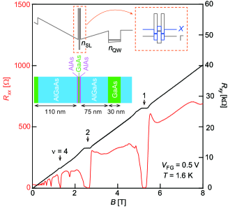
The sample consisted of a 30-nm-wide GaAs QW sandwiched between Al0.27Ga0.73As barriers, grown on an -type GaAs (001) substrate. The QW, with its center located 207 nm below the surface, was modulation doped on one side, with Si -doping ([Si] = m-2) at the center of the AlAs/GaAs/AlAs (2 nm/3 nm/2 nm) SL located 75 nm above the QW (inset of Fig. 1) Gardner et al. (2016). The Si -doping in the thin GaAs layer provides mobile electrons not only in the QW 75-nm away but also in the neighboring AlAs layers Umansky et al. (2009); Gardner et al. (2016); Manfra (2014); Chung et al. (2020); Friedland et al. (1996). The mobile electrons in the AlAs layers provide screening of the disorder potential created by the ionized Si donors. The wafer was processed into a 120-m-wide Hall bar with voltage-probe distance of 100 m and fitted with a Ti/Au front gate. The -type substrate was used as a back gate. Measurements were done at temperatures of – K using a standard lock-in technique.
Figure 1 shows the magnetotransport of the sample measured at 1.6 K. Here, we show data taken at a positive front gate voltage () of 0.5 V, which is supposed to increase the density of mobile electrons in the SL. Interestingly, despite the presence of mobile electrons in the SL, there are integer quantum Hall effects at Landau-level filling factor , and , where the longitudinal resistance () drops to zero and the Hall resistance () is quantized. From the Shubnikov-de Haas oscillations, we obtained a sheet carrier density of m-2, which agrees within 3% with the value deduced from the slope of . This suggests that, even if the SL contains conduction electrons, they apparently do not contribute to transport. We confirmed similar results for up to 0.8 V.
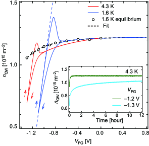
Figure 2 shows the dependence of the sheet carrier density deduced from at 0.2 T. The blue solid curve was obtained by sweeping at 1.6 K. As shown above, at 1.6 K the measured reflects exclusively the carrier density in the quantum well (), and not that in the SL. As we decreased from 0.8 V, remained almost constant for V (region I). This is consistent with the expectation that the SL contains mobile electrons, which screen the electric field from the front gate and thereby suppress its effect on . A distinct change in occurs only at V (region II), indicating that the screening capability of the SL is significantly decreased in region II. Upon increasing , we observed a pronounced hysteresis in region II, where changed at a faster rate, with an overshoot near the boundary with region I. The rate of change d/d m-2V-1 for the up sweep, shown by the blue dashed line, was consistent with the geometrical capacitance between the front gate and the center of the QW calculated from the distance (207 nm) and the permittivity of AlGaAs (). This implies that, upon increasing in region II, electrons accumulate only in the QW, resulting in a metastable state in which the QW (SL) is overpopulated (underpopulated) with respect to its equilibrium density. We conjecture that this results from the difficulty to inject charge into the SL once it becomes close to depletion and poorly conducting. The red curve in Fig. 2, obtained by sweeping at 4.3 K, shows similar behavior, while the boundary between regions I and II shifts to a more negative , with a smaller overshoot in the up sweep.
Turning our attention to region I, we notice that is not constant, but varies slightly with . This indicates that part of the electric field from the gate penetrates the SL populated with electrons. This is reasonable, as the SL is not a perfect metal; it has only a finite DOS, that is, a finite screening capability. In turn, by analyzing the change in with as shown later, we can quantify the DOS, and hence the screening capability, of the SL. (See Ref. Eisenstein et al. (1994) for the principle of this field-penetration technique.)
Even though we used a very slow sweep rate of 0.67 mV/sec to set , in region II gradually increased on a scale of several minutes to several tens of hours after was set at a constant value (inset of Fig. 2). This was the case even for down sweeps for which the system is closer to equilibrium. Similar temporal behavior was reported in Ref. Rössler et al. (2010). The transient time increased with decreasing temperature and decreasing . At V, equilibrium was not reached even after a few days at 4.3 K. We used the following method to determine the equilibrium value of at each , which is essential for evaluating the screening effect. First, we set at 4.3 K to facilitate the equilibration and waited until reached a steady value. Then, we decreased the temperature to 1.6 K and determined from the low-field . By repeating this process for different , we obtained as a function of , which we plot as open circles in Fig. 2. At V, we obtained the same value as that for the sweep. However, the difference between the two methods became significant at lower . We therefore employed the data obtained by the equilibration method for 0 V and those of the sweep for V and fit them using a double exponential function (the black dashed line in Fig. 2).
II.2 B. Circuit model
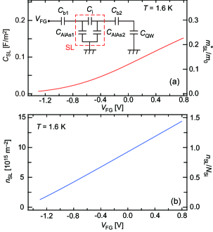
To deduce the excess electron density in the SL and thereby quantitatively characterize the screening effect, we analyzed the charge equilibration among the front gate, redtwo AlAs layers [AlAs1(2)] comprising the SL, and QW using the circuit model shown in the inset of Fig. 3(a). In addition to the geometrical capacitances between the neighboring elements among these (, , and ), the model contains the quantum capacitances of the QW () and the AlAs layers []. The quantum capacitance is expressed as , where / is the DOS ( is the electron effective mass, denotes QW or AlAs1(2), is the elementary charge, is the degeneracy, and /2 is the reduced Planck constant). , , and are calculated from the layer thicknesses and permittivity and is known from the effective mass of GaAs ( is the electron mass in vacuum) and the twofold spin degeneracy. This leaves the only unknown parameters in the model. For the model to be solvable, we need to assume that the two AlAs layers have the same density of states at the Fermi level, that is, (). We confirmed this assumption to be acceptable by noting that the calculated chemical potential difference between the two AlAs layers (up to 7 meV) was smaller than the disorder-broadened tail (a few tens of meV).
We calculate as a function of using the equilibrium relation between and obtained above. By numerically solving the circuit model with the value at each as an input, we can deduce as a function of , as shown in Fig. 3(a). decreases with decreasing , reflecting the disorder-broadened tail of the DOS. Interestingly, is not constant even at V, where it keeps increasing with . Since quantum capacitance is proportional to the DOS at the Fermi level, the obtained can be translated into the effective mass that would produce the same DOS for parabolic dispersion through the relation /. In thin AlAs layers, quantum confinement and strain split the three-fold valley degeneracy in bulk into one and two, with the former becoming lower in energy for a thickness below – nm Khisameeva et al. (2019); Van Kesteren et al. (1989). We therefore assumed , taking into account the spin degeneracy. The effective mass evaluated in this way is shown on the right axis of Fig. 3(a). In bulk AlAs, the effective masses in the transverse and longitudinal directions of the ellipsoid Fermi surface are and , respectively Vurgaftman et al. (2001). For AlAs QWs thinner than 6.0 nm, the 2DES occupies the lower non-degenerate valley, where experiments report a transverse mass of (–) Yamada et al. (1994); Momose et al. (1999); Vakili et al. (2004). The obtained /, which approaches the expected value (–) with increasing , is reasonable.
Once is obtained as a function of , one can calculate the electron density in the AlAs layers [] and SL (). Figure 3(b) shows the dependence of . The right axis of the figure indicates the excess electron density normalized by the doping density ( m-2). While varies almost linearly with , the slope decreases slightly at V.
II.3 C. Effects on mobility
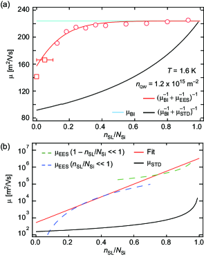
Now let us investigate the effect of screening on mobility. The symbols in Fig. 4(a) show the 1.6-K mobility () measured at the same carrier density ( m-2) but with the sample prepared to have different values. The open circles show data obtained by re-adjusting with the back gate after equilibrating the system at 4.3 K for (– V) and cooling the sample to 1.6 K. For this range, varied between 0.13 and 0.93 [see Fig. 3(b)]. As equilibration was not obtained for V at 4.3 K, we employed a different method to achieve smaller . The open squares in Fig. 4(a) show data obtained by applying V at room temperature and re-adjusting at 1.6 K with the back gate. We confirmed that the SL was already depleted (i.e., ) for V by noting that at 1.6 K the 2DES was depleted at zero back gate voltage. As Fig. 4(a) shows, decreased by 37% as decreased from 0.93 to 0.
We characterize the dependence by considering two main sources of disorder in modulation-doped GaAs 2DESs, i.e., background ionized impurities (BIs) and remote ionized impurities (RIs). For the mobility limited by RIs, we used the excess electron screening (EES) model proposed by Sammon et al. Sammon et al. (2018a). The dashed blue and green curves in Fig. 4(b) show the mobility calculated using the EES model for the two limits, and , respectively. The red curve is the fitting using the empirical formula derived in Ref. Sammon et al. (2018a). By adjusting the numerical parameters to connect the two limits, we obtain
| (1) |
Here, is the Fermi wave number and nm is the center-to-center distance between the QW and SL. The red curve in Fig. 4(a) shows the least-squares fit of the total mobility // based on Matthiessen’s rule, where is the only parameter and we assumed it to be constant. The value obtained from the fit is shown by the cyan line in Fig. 4(a). The EES model well explains the overall dependence of the measured , providing good agreement for . For , the agreement between the experiment and model becomes less satisfactory, which is because we tried to fit both regimes of and using Eq. (1) [Fig. 4(b)]. For comparison, we also calculated the mobility using the standard model () Hirakawa and Sakaki (1986), assuming independent scattering by () ionized donors. The black lines in Figs. 4(b) and 4(a) show and the resultant total mobility , respectively. The independent-scattering model predicts a mobility way below the experimental result, which in turn demonstrates the importance of the screening by excess electrons.
We also examined the possibility of excess electrons in the SL affecting . Sammon et al. reported that, for strong screening, the contribution of BIs to is canceled out by the image-charge effect when they are located farther than from the center of the QW Sammon et al. (2018b). We calculated by integrating contributions from BIs over different spatial ranges, and . The difference between the two cases is less than 1%, thus corroborating our assumption of constant .
II.4 D. Quantum lifetime
Finally, let us investigate the effect of screening on quantum lifetime () deduced from Shubnikov–de Haas (SdH) oscillations, a quantity often argued to be a better indicator of sample quality than mobility in terms of FQHEs. Figure 5(a) shows the SdH oscillations measured at 0.27 K at a constant carrier density ( m-2) under different screening conditions of , , and (corresponding of 0, , and V, respectively). Under the well-screened condition (), minima at odd filling factors due to spin splitting are more pronounced, indicating the influence of screening. We extracted the quantum lifetime by using the functional form of SdH oscillations, given as Coleridge (1991)
| (2) |
with
| (3) |
Here, is the amplitude of the SdH oscillations, is the cyclotron frequency, is the at zero magnetic field, is a thermal damping factor, and is the Boltzmann constant. Thus, the slope of / vs. , known as a Dingle plot, shown in the inset of Fig. 5(a) gives the quantum lifetime 111 For the data in the weak screening regime taken with V set at room temperature, analysis taking into account density inhomogeneity Qian et al. (2017) was necessary to fit the Dingle plot with the correct intercept of 4 at . The density inhomogeneity derived from the fit was 0.6 and 1.8% for and V, respectively. . The obtained is shown by open symbols in Fig. 5(b). In contrast to , or transport lifetime (), does not show a discernible change as a function of .
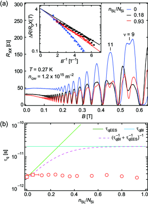
We compared the measured with the calculated quantum lifetimes limited by RIs and BIs ( and ), which are shown in Fig. 5(b) by the green and cyan lines, respectively. Here, was calculated with the EES model Sammon et al. (2018a), whereas was calculated with the independent-scattering model using the BI concentration obtained from ( m2/Vs). The expected total quantum lifetime is shown by the dashed magenta line. Although the measured is close to the values expected in the weak screening regime, it remains about ps when increases, much lower than expected in the intermediate and strong screening regimes. This discrepancy was not mitigated even when a more elaborate model was employed, such as one with different BI concentrations in the GaAs QW and AlGaAs barrier layers Sammon et al. (2018b) and remote charges on the sample surface and the back gate Chen et al. (2012); Wang et al. (2013). Extrinsic mechanisms that might reduce the apparent quantum lifetime, such as the finite density gradient Qian et al. (2017) 222An attempt to fit the Dingle-plot data in Fig. 5(a) using the density-gradient model in Ref. Qian et al. (2017) together with the calculated quantum lifetime resulted in a strongly nonlinear curve, which did not fit the experimental results. and the response time of the lock-in amplifier 333Reducing the field sweep rate from 10 mT/sec (which we normally use) to 10 T/sec did not affect the measured value of ., did not explain the discrepancy, either. Ultra-high-quality samples with much longer , such as those in Refs. Qian et al. (2017); Fu et al. (2018), might be necessary to observe the predicted screening effect on . Yet, it is interesting that the visibility of the spin gap varies with even when remains constant, as we observed. For , the density inhomogeneity estimated from the analysis of the Dingle plot Qian et al. (2017) is 1.8%, which may be partly responsible for the poorly developed quantum Hall effects at even as well as odd integer fillings. However, for and , the estimated density inhomogeneity is less than 0.2% with no clear difference, which cannot account for the difference in the visibility of the spin gap. This suggests that the screening of long-range disorder becomes more important for interaction phenomena such as FQHEs. The broad minimum around T seen in Fig. 1 is a precursor of the FQHE. By investigating FQHEs at lower temperatures under different screening conditions, it will be possible to examine how the energy gap of FQHEs is correlated with the composite fermion mobility Kang et al. (1995) deduced from the resistivity at .
III III. CONCLUSION
In summary, we investigated the screening effects of SL doping on the mobility and quantum lifetime of a GaAs 2DES by controlling the excess electron density in the SL with a top gate. The dependence of mobility on excess electron density is consistent with theory taking into account the screening effect. On the other hand, the measured quantum mobility was much lower than expected from theory and did not show a discernible change with excess electron density. The excess electrons also affected the depth of the spin-gap minima in the Shubnikov-de Haas oscillations, which suggests the possibility of controlling the visibility of FQHEs in-situ.
IV ACKNOWLEDGEMENTS
The authors thank M. Kamiya and H. Irie for support in the measurements, H. Murofushi for processing the device. and M. A. Zudov for helpful discussions. This work was supported by a JSPS KAKENHI Grant, No. JP15H05854.
References
- Pfeiffer and West (2003) L. Pfeiffer and K. W. West, “The role of MBE in recent quantum Hall effect physics discoveries,” Physica E 20, 57 (2003).
- Umansky et al. (2009) V. Umansky, M. Heiblum, Y. Levinson, J. Smet, J. Nübler, and M. Dolev, “MBE growth of ultra-low disorder 2DEG with mobility exceeding ,” J. Cryst. Growth 311, 1658 (2009).
- Gardner et al. (2016) G. C. Gardner, S. Fallahi, J. D. Watson, and M. J. Manfra, “Modified MBE hardware and techniques and role of gallium purity for attainment of two dimensional electron gas mobility in AlGaAs/GaAs quantum wells grown by MBE,” J. Cryst. Growth 441, 71 (2016).
- Manfra (2014) M. J. Manfra, “Molecular Beam Epitaxy of Ultra-High-Quality AlGaAs/GaAs Heterostructures: Enabling Physics in Low-Dimensional Electronic Systems,” Annu. Rev. Condens. Matter Phys. 5, 347 (2014).
- Chung et al. (2020) Y. J. Chung, K. A. Villegas Rosales, K. W. Baldwin, K. W. West, M. Shayegan, and L. N. Pfeiffer, “Working principles of doping-well structures for high-mobility two-dimensional electron systems,” Phys. Rev. Mater. 4, 44003 (2020).
- Willett et al. (1988) R. L. Willett, H. L. Stormer, D. C. Tsui, L. N. Pfeiffer, K. W. West, and K. W. Baldwin, “Termination of the series of fractional quantum hall states at small filling factors,” Phys. Rev. B 38, 7881 (1988).
- Goldman et al. (1990) V. J. Goldman, M. Santos, M. Shayegan, and J. E. Cunningham, “Evidence for two-dimentional quantum Wigner crystal,” Phys. Rev. Lett. 65, 2189 (1990).
- Lilly et al. (1999) M. P. Lilly, K. B. Cooper, J. P. Eisenstein, L. N. Pfeiffer, and K. W. West, “Evidence for an anisotropic state of two-dimensional electrons in high landau levels,” Phys. Rev. Lett. 82, 394 (1999).
- Du et al. (1999) R. R. Du, D. C. Tsui, H. L. Stormer, L. N. Pfeiffer, K. W. Baldwin, and K. W. West, “Strongly anisotropic transport in higher two-dimensional landau levels,” Solid State Commun. 109, 389 (1999).
- Suen et al. (1992) Y. W. Suen, L. W. Engel, M. B. Santos, M. Shayegan, and D. C. Tsui, “Observation of a = 1/2 fractional quantum Hall state in a double-layer electron system,” Phys. Rev. Lett. 68, 1379 (1992).
- Tsui et al. (1982) D. C. Tsui, H. L. Stormer, and A. C. Gossard, “Two-dimensional magnetotransport in the extreme quantum limit,” Phys. Rev. Lett. 48, 1559 (1982).
- Willett et al. (1987) R. Willett, J. P. Eisenstein, H. L. Störmer, D. C. Tsui, A. C. Gossard, and J. H. English, “Observation of an even-denominator quantum number in the fractional quantum Hall effect,” Phys. Rev. Lett. 59, 1776 (1987).
- Pan et al. (2011) W. Pan, N. Masuhara, N. S. Sullivan, K. W. Baldwin, K. W. West, L. N. Pfeiffer, and D. C. Tsui, “Impact of disorder on the 5/2 fractional quantum Hall state,” Phys. Rev. Lett. 106, 206806 (2011).
- Gamez and Muraki (2013) G. Gamez and K. Muraki, “ = 5/2 fractional quantum Hall state in low-mobility electron systems: Different roles of disorder,” Phys. Rev. B 88, 075308 (2013).
- Friedland et al. (1996) K. J. Friedland, R. Hey, H. Kostial, R. Klann, and K. Ploog, “New concept for the reduction of impurity scattering in remotely doped GaAs quantum wells,” Phys. Rev. Lett. 77, 4616 (1996).
- Sammon et al. (2018a) M. Sammon, M. A. Zudov, and B. I. Shklovskii, “Mobility and quantum mobility of modern GaAs/AlGaAs heterostructures,” Phys. Rev. Mater. 2, 104001 (2018a).
- Sammon et al. (2018b) M. Sammon, M. A. Zudov, and B. I. Shklovskii, “Mobility and quantum mobility of modern GaAs/AlGaAs heterostructures,” Phys. Rev. Mater. 2, 064604 (2018b).
- Rössler et al. (2010) C. Rössler, T. Feil, P. Mensch, T. Ihn, K. Ensslin, D. Schuh, and W. Wegscheider, “Gating of high-mobility two-dimensional electron gases in GaAs/AlGaAs heterostructures,” New J. Phys. 12, 043007 (2010).
- Dmitriev et al. (2012) D. V. Dmitriev, I. S. Strygin, A. A. Bykov, S. Dietrich, and S. A. Vitkalov, “Transport relaxation time and quantum lifetime in selectively doped GaAs/AlAs heterostructures,” JETP Letters 95, 420 (2012).
- Peters et al. (2017) S. Peters, L. Tiemann, C. Reichl, S. Fält, W. Dietsche, and W. Wegscheider, “Improvement of the transport properties of a high-mobility electron system by intentional parallel conduction,” Appl. Phys. Lett. 110, 042106 (2017).
- Eisenstein et al. (1994) J. P. Eisenstein, L. N. Pfeiffer, and K. W. West, “Compressibility of the two-dimensional electron gas: Measurements of the zero-field exchange energy and fractional quantum Hall gap,” Phys. Rev. B 50, 1760 (1994).
- Khisameeva et al. (2019) A. R. Khisameeva, A. V. Shchepetilnikov, V. M. Muravev, S. I. Gubarev, D. D. Frolov, Yu A. Nefyodov, I. V. Kukushkin, C. Reichl, W. Dietsche, and W. Wegscheider, “Achieving balance of valley occupancy in narrow AlAs quantum wells,” J. Appl. Phys. 125, 154501 (2019).
- Van Kesteren et al. (1989) H. W. Van Kesteren, E. C. Cosman, P. Dawson, K. J. Moore, and C. T. Foxon, “Order of the X conduction-band valleys in type-II GaAs/AlAs quantum wells,” Phys. Rev. B 39, 13426 (1989).
- Vurgaftman et al. (2001) I. Vurgaftman, J. R. Meyer, and L. R. Ram-Mohan, “Band parameters for III-V compound semiconductors and their alloys,” J. Appl. Phys. 89, 5815 (2001).
- Yamada et al. (1994) S. Yamada, K. Maezawa, W. T. Yuen, and R. A. Stradling, “X-conduction-electron transport in very thin alas quantum wells,” Phys. Rev. B 49, 2189 (1994).
- Momose et al. (1999) H. Momose, N. Mori, C. Hamaguchi, T. Ikaida, H. Arimoto, and N. Miura, “Cyclotron resonance in (GaAs)n/(AlAs)n superlattices under ultra-high magnetic fields,” Physica E 4, 286 (1999).
- Vakili et al. (2004) K. Vakili, Y. P. Shkolnikov, E. Tutuc, E. P. De Poortere, and M. Shayegan, “Spin susceptibility of two-dimensional electrons in narrow AlAs quantum wells,” Phys. Rev. Lett. 92, 226401 (2004).
- Hirakawa and Sakaki (1986) K. Hirakawa and H. Sakaki, “Mobility of the two-dimensional electron gas at selectively doped -type AlxGa1-xAs/GaAs heterojunctions with controlled electron concentrations,” Phys. Rev. B 33, 8291 (1986).
- Coleridge (1991) P. T. Coleridge, “Small-angle scattering in two-dimensional electron gases,” Phys. Rev. B 44, 3793 (1991).
- Note (1) For the data in the weak screening regime taken with V set at room temperature, analysis taking into account density inhomogeneity Qian et al. (2017) was necessary to fit the Dingle plot with the correct intercept of 4 at . The density inhomogeneity derived from the fit was 0.6 and 1.8% for and V, respectively.
- Chen et al. (2012) J. C. H. Chen, D. Q. Wang, O. Klochan, A. P. Micolich, K. Das Gupta, F. Sfigakis, D. A. Ritchie, D. Reuter, A. D. Wieck, and A. R. Hamilton, “Fabrication and characterization of ambipolar devices on an undoped AlGaAs/GaAs heterostructure,” Appl. Phys. Lett. 100, 052101 (2012).
- Wang et al. (2013) D. Q. Wang, J. C. H. Chen, O. Klochan, K. Das Gupta, D. Reuter, A. D. Wieck, D. A. Ritchie, and A. R. Hamilton, “Influence of surface states on quantum and transport lifetimes in high-quality undoped heterostructures,” Phys. Rev. B 87, 195313 (2013).
- Qian et al. (2017) Q. Qian, J. Nakamura, S. Fallahi, G. C. Gardner, J. D. Watson, S. Lüscher, J. A. Folk, G. A. Csáthy, and M. J. Manfra, “Quantum lifetime in ultrahigh quality GaAs quantum wells: Relationship to and impact of density fluctuations,” Phys. Rev. B 96, 035309 (2017).
- Note (2) An attempt to fit the Dingle-plot data in Fig. 5(a) using the density-gradient model in Ref. Qian et al. (2017) together with the calculated quantum lifetime resulted in a strongly nonlinear curve, which did not fit the experimental results.
- Note (3) Reducing the field sweep rate from 10 mT/sec (which we normally use) to 10 T/sec did not affect the measured value of .
- Fu et al. (2018) X. Fu, A. Riedl, M. Borisov, M. A. Zudov, J. D. Watson, G. Gardner, M. J. Manfra, K. W. Baldwin, L. N. Pfeiffer, and K. W. West, “Effect of illumination on quantum lifetime in GaAs quantum wells,” Phys. Rev. B 98, 195403 (2018).
- Kang et al. (1995) W. Kang, Song He, H. L. Stormer, L. N. Pfeiffer, K. W. Baldwin, and K. W. West, “Temperature dependent scattering of composite fermions,” Phys. Rev. Lett. 75, 4106 (1995).