Multiband charge density wave exposed in a transition metal dichalcogenide
In the presence of multiple bands, well-known electronic instabilities may acquire new complexity. While multiband superconductivity is the subject of extensive studies, the possibility of multiband charge density waves (CDWs) has been largely ignored so far. Here, combining energy dependent scanning tunnelling microscopy (STM) topography with a simple model of the charge modulations and a self-consistent calculation of the CDW gap, we find evidence for a multiband CDW in 2H-NbSe2. This CDW not only involves the opening of a gap on the inner band around the K-point, but also on the outer band. This leads to spatially out-of-phase charge modulations from electrons on these two bands, which we detect through a characteristic energy dependence of the CDW contrast in STM images.
Imposing a new periodicity on a crystal leads to the reorganization of the electronic bands of the parent compound through their back-folding on the new Brillouin zone. New periodicities may be engineered in designer materials, for instance in artificial heterostructures with Moiré minigaps, or emerge due to a structural or electronic phase transition. The charge density wave state is an electronic order where the charge density develops a spatial modulation concomitantly to a periodic distortion of the atomic lattice and the opening of a gap in the quasi-particle spectrum. By reducing the electronic band energy, this gap compensates for the elastic and Coulomb energy costs associated with the formation of the CDW. It also lowers the degeneracy of the electronic states at the crossings of the folded bands. These are the points in the band structure of the parent compound that are connected by the wavevector of the new periodicity. Although a gap should open at all the crossings of the folded bands, previous studies only focused on the primary CDW gap around the Fermi-level, which leads to the highest energy gain of the reconstructed system. The existence of secondary gaps and associated charge modulations remains largely unexplored.
In many cases, only a tiny fraction of the electrons are involved in the CDW formation. Therefore, the CDW gap manifests only as a slight reduction of the density of states (DOS) -which can depend on momentum- rather than a full depletion of the DOS. This makes it challenging to measure the CDW gap using spectroscopic probes such as angle resolved photoemission spectroscopy (ARPES) and scanning tunnelling spectroscopy (STS). This is particularly true for 2H-NbSe2 [1, 2, 3, 4, 5] (hereinafter simply NbSe2). However, the effect of the redistributed electrons can be readily detected in topographic STM images, even for minute changes brought upon by the opening of the CDW gap as demonstrated in the following.
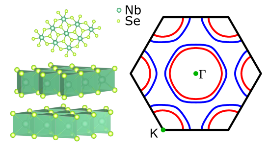
NbSe2 is an iconic material of correlated electron physics. It hosts a nearly-commensurate charge density wave below K and a superconducting (SC) order below K [6, 7, 8, 9, 10]. NbSe2 is a layered material with a three-fold symmetric crystal structure around the direction perpendicular to the layers (Fig. 1). Each unit cell is composed of two slabs of Se-Nb-Se trilayers, where the Se lattices are 60∘ rotated, while the Nb atoms are aligned on top of each other in a trigonal prismatic coordination with the Se atoms.
The Fermi surface (FS) of NbSe2 is mainly determined by the bonding and antibonding combinations of the Nb-4d orbitals [11, 12] leading to double-walled barrel-shaped pockets around the K and points of the hexagonal Brillouin-zone [13, 14, 2, 3] (Fig. 1). The charge ordered state consists of three CDWs which form along the three equivalent directions with wavevectors , where and depends on temperature [10]. In real space, this yields a locally commensurate superstructure delimited by discommensurations [15, 16], where is the atomic periodicity.
The reconstruction is readily accessible to topographic STM imaging. Its bias dependent contrast has been the focus of previous studies, with particular emphasis on the contrast inversion expected in a classic Peierls scenario between images acquired above and below the CDW gap [17, 18], and on the role of defects in stabilizing the CDW [5]. Sacks et al. [18] calculate the bias dependence of the CDW phase in a perturbative approach, considering a single band normal state description of NbSe2. They find that the phase-shift of the CDW component of the local DOS can be very different from the 180∘ expected in a one-dimensional (1D) case (Supplemental Material Sec. LABEL:SupSec:LDOS_1D_CDW) when changing the imaging bias across the Fermi level (). However, their model does not reproduce the full bias dependence of the CDW amplitude and phase that we find.
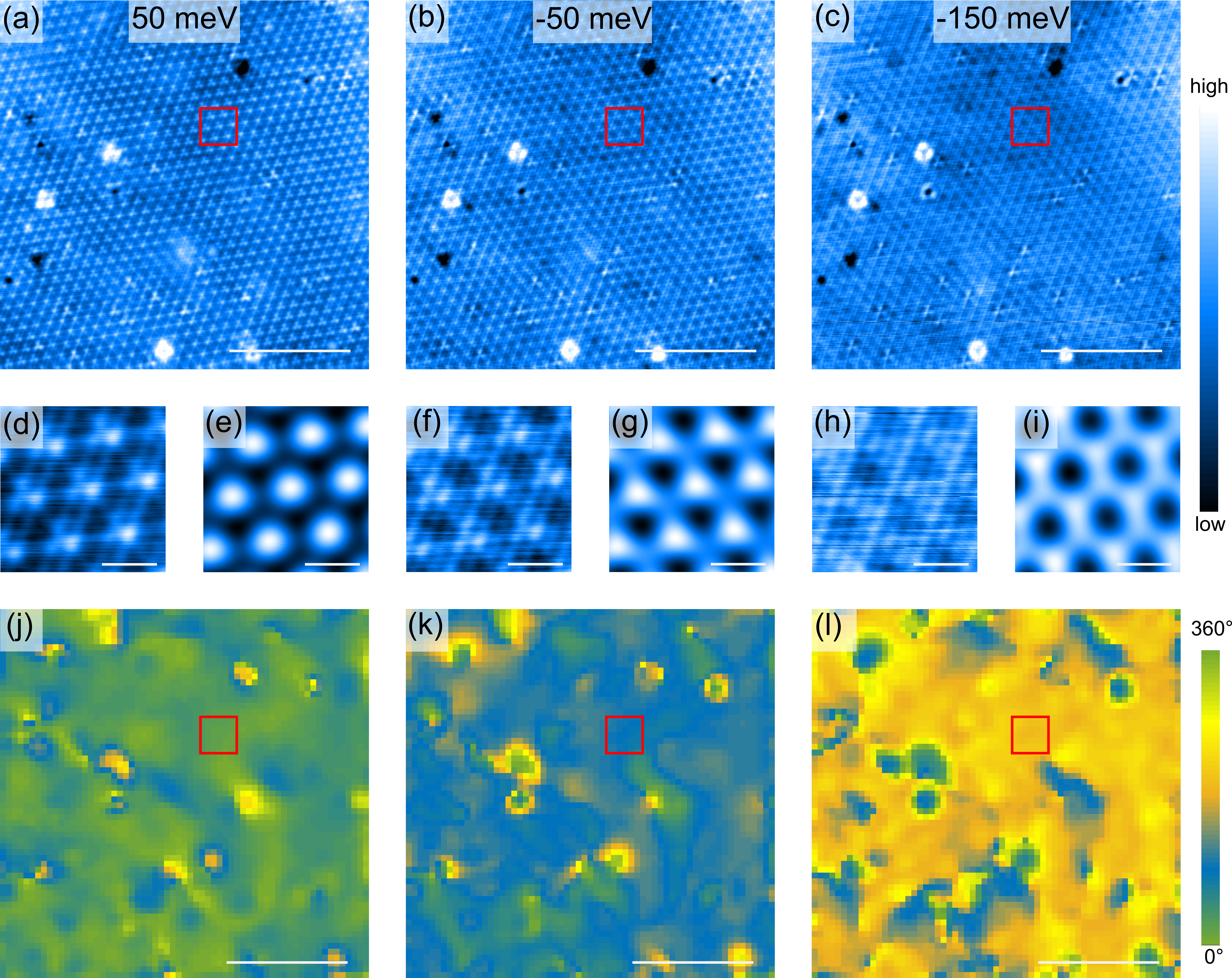
In Figs. 2(a)-(c), we present a selection from numerous topographic STM images of the same region on a cleaved NbSe2 surface at different sample biases () between V and V. They show a triangular atomic lattice with a superimposed CDW modulation (see also Suppl. Fig. LABEL:fig:suppl_atomic_lattice(a)), consistent with previous STM studies of unstrained bulk NbSe2 [17, 4, 5, 21, 22, 23, 24, 16]. A defect free region with a well resolved CDW outlined in red is magnified in Figs. 2(d), (f) and (h) for each . In order to identify the origin of the bias dependence of the topographic contrast in these images, we separate the atomic lattice and CDW contributions using Fourier filtering (Supplemental Material Sec. LABEL:SupSec:atomic_STM). This analysis shows that the bias dependent STM contrast is due to the changing CDW signal (Fig. 2(e), (g) and (i)), since the corresponding atomic lattice contrast remains unchanged (see Suppl. Fig. LABEL:fig:suppl_atomic_lattice).
The observed CDW pattern can be modeled as the sum of three plane waves as described in Ref [16]. While each plane wave has its own phase , which depends on a selected reference point, the dephasing parameter is uniquely defined for each particular CDW pattern, independent of any reference point. represents the internal CDW structure, quantifying the local relative position of the wavefronts of the three CDWs. In Figs. 2(j)-(l), we show corresponding to the STM images in Figs. 2(a)-(c), respectively. They were obtained by fitting the CDW contrast following the method described in Ref. [16].
Each bias voltage is characterized by a dominant dephasing parameter (Figs. 2(j)-(l)), except in the vicinity of defects discussed later. This visual assessment is confirmed by the peaked histograms of (Suppl. Fig. LABEL:fig:suppl_dephasing_histogram)). Fitting a Gaussian to these histograms allows to extract a well defined dephasing parameter for each imaging bias (Suppl. Fig. LABEL:fig:suppl_dephasing_mapping). For a quantitative analysis of the bias dependence of , we note that a given local CDW structure is represented by any arbitrary combination of summing up to the same dephasing parameter, in particular the one where all three phases are equal. Moreover, the threefold symmetry of the system implies there is no privileged plane wave among the three used to describe the CDW. These observations allow us to map the problem to a one-dimensional (1D) description with an apparent CDW phase (Supplemental Material Sec. LABEL:SupSec:dephasing_parameter_measured), and model to understand the bias dependent CDW pattern.
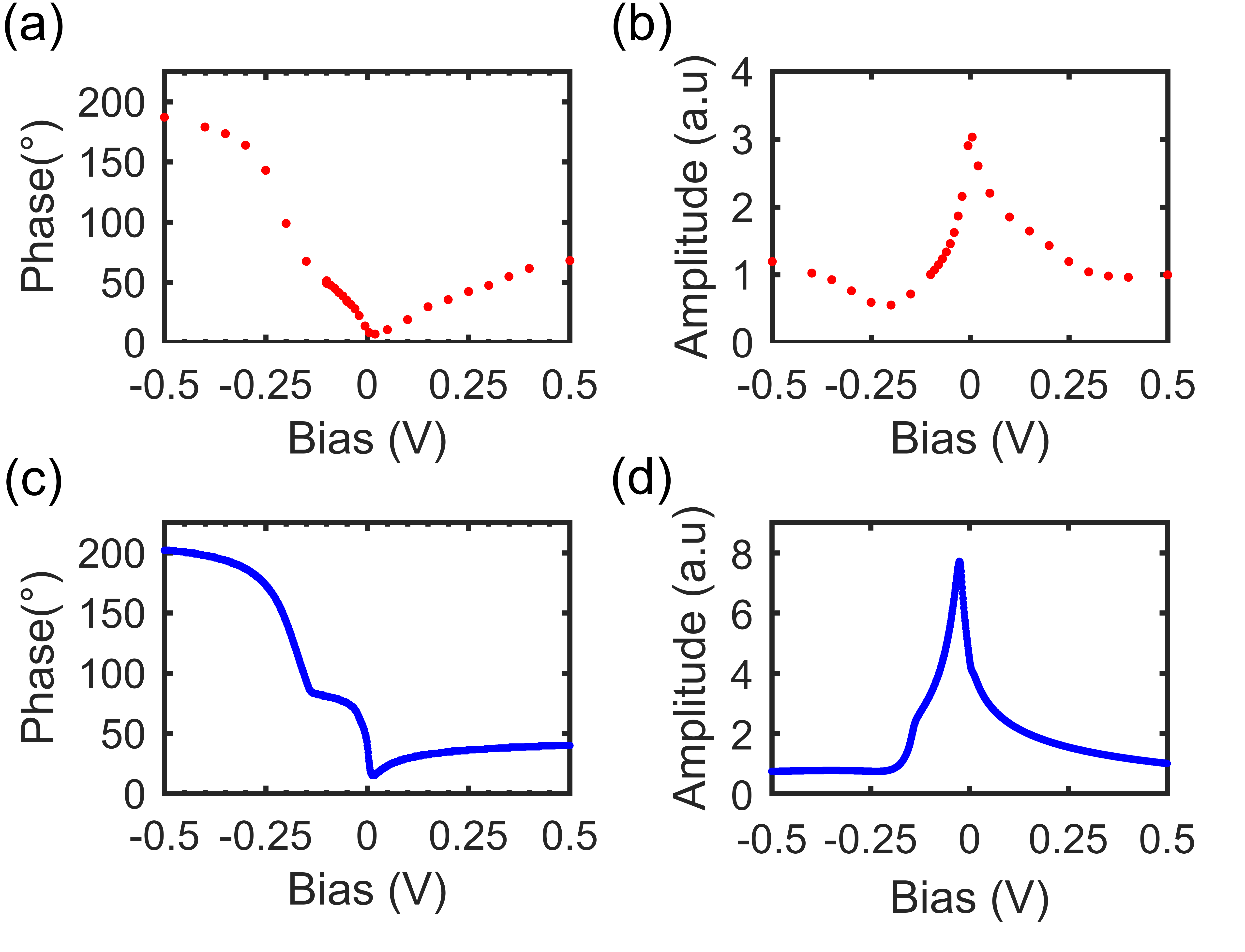
Plotting in Fig. 3(a) reveals a striking non-monotonic bias dependence, with an inflexion point around V and a minimum slightly above the Fermi-level ( V). This dependence is robust as long as is extracted from topographic STM images away from defects (Suppl. Fig. LABEL:fig:suppl_away_from_defect). Close to defects, the dephasing parameter is different and tends to depend much less on imaging bias (Suppl. Fig. LABEL:fig:suppl_around_defects). This is consistent with earlier findings that defects (and impurities) can act as strong pinning centers [25, 26] locking the local phase of the CDW or driving the formation of CDW domains [27, 28].
The CDW amplitude can be extracted in a similar way to the phase, by fitting the histogram of the local amplitudes of each plane wave measured over the entire field of view with a Gaussian, and extracting the peak value . The bias dependence and magnitude of is nearly the same for all three CDWs (Suppl. Fig. LABEL:fig:suppl_amplitude(b)). For the analysis, we consider the average of these three amplitudes at each bias plotted in Fig. 3(b).
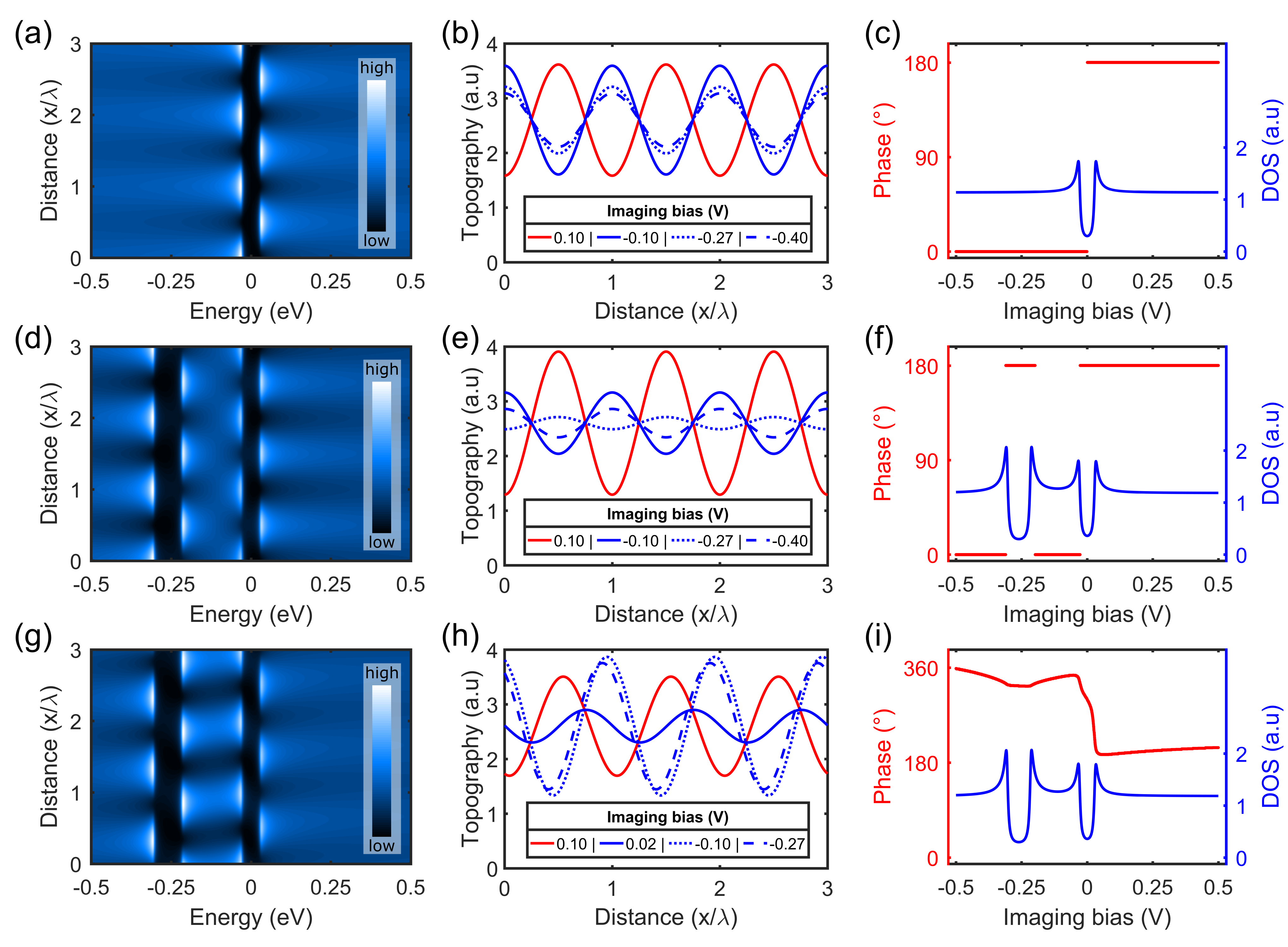
To understand the bias dependence of the CDW amplitude and phase in Fig. 3, we simulate topographic STM traces using a 1D model system (Supplemental Material Sec. LABEL:SupSec:constant_current_topo). In the simplest configuration corresponding to the Peierls reconstruction, we consider the contribution to the tunneling current of a single charge modulation (CM) and its associated gap centered on EF (Fig. 4(a)-(c)). In this case, traces at the same polarity are always in phase, whereas traces at opposite polarities always show contrast inversion (or a 180∘ phase shift in the present harmonic model). The latter, often considered as an identifying hallmark of the CDW state [29], clearly does not reproduce the data in Fig. 3(a).
A single CM can only produce two sets of STM traces differing by contrast inversion in the vicinity of the gap. To generate a more complex bias dependence of the phase, we consider the possibility of a second CM whose associated gap opens in another band and away from (Fig. 4(d)-(f)). If these two harmonic CMs are in phase (Fig. 4(d)), the resulting STM traces are either in-phase or 180∘ out of phase ((Fig. 4(e)), unable to reproduce the data in Fig. 3(a). To generate more structures in the bias dependence of the phase, we need to introduce a phase shift between the two CMs (Fig. 4(g)-(i)). This leads to a phase which is no longer bi-modal, limited to two values differing by 180∘ as in (Figs. 4(c)-(f)). It takes many different values (Fig. 4(i)), where the precise bias dependence is defined by the magnitude of the two gaps, their position relative to and by the relative phase shift between the two CMs. The simulated STM topographic traces in Fig. 4(b)(e) and (h) also reveal a pronounced bias dependent imaging amplitude with distinct line-shapes in the three model cases discussed above (Suppl. Fig. LABEL:fig:suppl_amplitude_in_models).
The broad parameter space of our 1D model makes it challenging to run a self converging fit to the data. Visually optimizing the size and position of the two gaps in Fig. 4(i), we find a range of parameters (Supplemental Material Sec. LABEL:SupSec:two_gap) simultaneously reproducing the experimental bias dependent CDW phase and amplitude data remarkably well (Fig. 3). As for the relative phase between the two CMs, it is chosen to minimize the Coulomb interaction of the CMs and to conform with the strong commensuration energy that locally locks them to the lattice. Reducing the Coulomb energy is obtained by introducing a phase shift between the two CMs, which can only be ((Fig. 4(g)) to satisfy the lock-in criterion with the lattice given the 3a0 periodicity of the CDW.
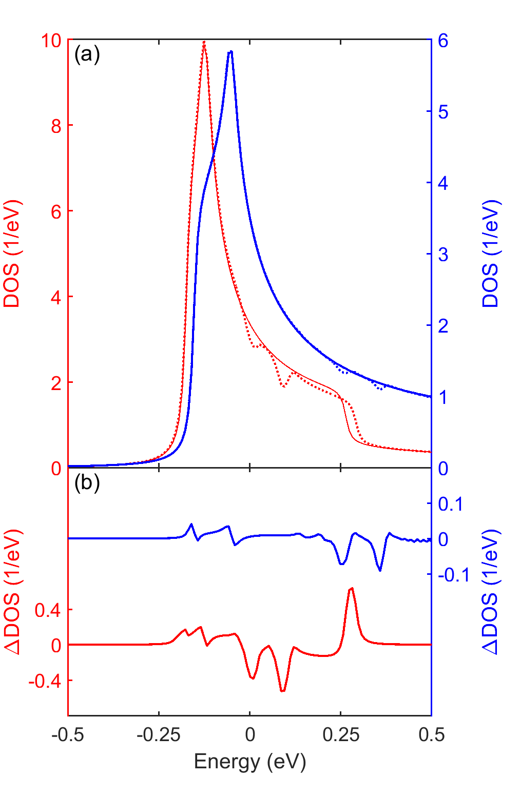
In the following, we turn to theoretically modelling multiple CDW gaps on different bands in NbSe2. We deploy self-consistent calculations to include the CDW gap within the random phase approximation on the two-dimensional two-band tight-binding fit to the NbSe2 band structure constrained by ARPES [3]. The corresponding Fermi surface shown in Fig. 1 consists of inner (red) and outer (blue) bands originating from symmetric and antisymmetric combinations of the Nb d orbitals. The model (see Methods) was previously shown to accurately reproduce the full range of experimental measurements on the charge-ordered state [12, 30]. The resulting DOS for the gapped and ungapped cases in each band are shown in Fig. 5(a). To emphasize the DOS reduction accompanying the CDW phase transition, we plot the difference between the gapped and ungapped DOS for each band in Fig. 5(b).
Our theoretical modelling shows a clear gap on the inner band at , consistent with the gap measured by ARPES around the -point [3]. Interestingly, Fig. 5(b) reveals further DOS reductions, for example near 100 meV on the inner band and -50 meV on the outer band. These features are indicative of CDW gaps opening away from EF in addition to the (primary) gap at EF, backing the simple model we propose to understand the bias dependence of the CDW appearance in STM images of NbSe2. According to Fig. 5(b), there could even be more than two gaps. Consequently, we have included up to gaps to our 1D model. However, the agreement with the data is similar for and (Supplemental Material Sec. LABEL:SupSec:three_gap), and we see no improvements adding more gaps.
In summary, the remarkable match between the bias dependence of the CDW contrast in STM topography and the simple 1D model proposed here provides compelling evidence that the CDW in NbSe2 is composed of at least two out-of-phase CMs on the inner and outer bands. While a 180∘ phase shift between these two CMs would minimise the Coulomb energy, the complex bias dependence of the CDW amplitude and phase observed by STM can only be reproduced when considering also the commensuration energy. This highlights the importance of the coupling of charge order to the lattice, which manifests in the formation of discommensurations [15, 16] and ultimately enables the observation of the multiband CMs uncovered here. The present study further highlights the power of topographic imaging to gain unique insight into detailed features of the CDW too faint to be detected accurately by tunneling spectroscopy. The formation of multiple modulations in response to new periodicities of a primary transition directly observed here, is extremely general and should in principle be present in all charge (and spin) density wave materials, and suggests new directions to explore in the physics of spatially modulated electronic orders.
I Methods
Crystal growth and STM measurements. Single crystals of NbSe2 were grown via iodine assisted chemical vapour transport and cleaved in-situ at room temperature. STM experiments were done in UHV (base pressure below mbar) using tips mechanically cut from a PtIr wire and conditioned in-situ on a clean Ag(111) single crystal. The bias voltage was applied to the sample. STM images were recorded in constant current mode with at least 64 pixel/nm resolution. Details of the CDW amplitude and phase fitting procedure can be found in Ref [16].
Self-consistent calculations. We modeled the CDW gap in the NbSe2 bandstructure using the random phase approximation. Our model is based on a structured electron-phonon coupling dependent on the ingoing and outgoing electron momenta and the orbital character of the two bands scattered between; details are provided in Refs. [12, 30]. This model, which has as its only free parameter the overall magnitude of the electron-phonon coupling (constrained by =33.5K), has previously been shown to agree well with the full range of experimental observations on the charge ordered state in NbSe2. Using the Nambu Gor’kov method we solved for the CDW gap self-consistently at a set of high-symmetry points in the Brillouin zone, using the results to constrain a second tight-binding fit for the k-dependent CDW gap. We modeled the backfolding of the electronic bands using an approximate commensurate 33 CDW geometry. A CDW gap at the Fermi level is observed in ARPES predominantly at points along the inner K-pocket, and our model reproduces this result. However, additional small gaps are also expected to open wherever band crossings are introduced by the backfolding (and where the CDW gap is nonzero), even at energies away from the Fermi level. This is the origin of the suppression of DOS at energies below EF seen in Fig. 5.
II Acknowledgments
We acknowledge A. F. Morpurgo and I. Maggio-Aprile for inspiring discussions. We thank A. Guipet and G. Manfrini for their technical support in the STM laboratories. This project was supported by Div.2 (Grant No. 182652) and Sinergia (Grant No. 147607) of the Swiss National Science Foundation. F. F. acknowledges support from the Astor Junior Research Fellowship of New College, Oxford.
III Author contributions
C.R. designed the experiment. M.S. and A.S. took care of the STM experiments. Á.P performed the data analysis. F.F. and J.v.W. performed the self-consistent calculations. Á.P. did the one-dimensional model simulations. C.B. and E.G. synthesized the bulk crystals. Á.P, A.S., F.F, J.v.W. and C.R. wrote the paper. All authors contributed to the scientific discussions and manuscript revisions.
IV Competing interests
The authors declare no competing interests.
References
- Wang et al. [1990] C. Wang, B. Giambattista, C. G. Slough, R. V. Coleman, and M. A. Subramanian, Energy gaps measured by scanning tunneling microscopy, Physical Review B 42, 8890 (1990).
- Borisenko et al. [2009] S. V. Borisenko, A. A. Kordyuk, V. B. Zabolotnyy, D. S. Inosov, D. Evtushinsky, B. Büchner, A. N. Yaresko, A. Varykhalov, R. Follath, W. Eberhardt, L. Patthey, and H. Berger, Two energy gaps and fermi-surface “arcs” in NbSe2, Physical Review Letters 102, 166402 (2009).
- Rahn et al. [2012] D. J. Rahn, S. Hellmann, M. Kalläne, C. Sohrt, T. K. Kim, L. Kipp, and K. Rossnagel, Gaps and kinks in the electronic structure of the superconductor 2H-NbSe2 from angle-resolved photoemission at 1 K, Physical Review B 85, 224532 (2012).
- Soumyanarayanan et al. [2013] A. Soumyanarayanan, M. M. Yee, Y. He, J. van Wezel, D. J. Rahn, K. Rossnagel, E. W. Hudson, M. R. Norman, and J. E. Hoffman, Quantum phase transition from triangular to stripe charge order in NbSe2, Proc. Natl. Acad. Sci. 110, 1623 (2013).
- Arguello et al. [2014] C. J. Arguello, S. P. Chockalingam, E. P. Rosenthal, L. Zhao, C. Gutiérrez, J. H. Kang, W. C. Chung, R. M. Fernandes, S. Jia, A. J. Millis, R. J. Cava, and A. N. Pasupathy, Visualizing the charge density wave transition in 2H-NbSe2 in real space, Phys. Rev. B 89, 235115 (2014).
- Revolinsky et al. [1965] E. Revolinsky, G. A. Spiering, and D. J. Beerntsen, Superconductivity in the niobium-selenium system, Journal of Physics and Chemistry of Solids 26, 1029 (1965).
- Wilson et al. [1975] J. A. Wilson, F. J. Di Salvo, and S. Mahajan, Charge-density waves and superlattices in the metallic layered transition metal dichalcogenides, Advances in Physics 24, 117 (1975).
- Harper et al. [1975] J. M. E. Harper, T. H. Geballe, and F. J. Di Salvo, Heat capacity of 2H-NbSe2 at the charge density wave transition, Physics Letters A 54, 27 (1975).
- Long et al. [1977] J. R. Long, S. P. Bowen, and N. E. Lewis, Anomalous resistivity of iodine-free 2H-NbSe2, Solid State Communications 22, 363 (1977).
- Moncton et al. [1975] D. E. Moncton, J. D. Axe, and F. J. DiSalvo, Study of superlattice formation in 2H-NbSe2 and 2H-TaSe2 by neutron scattering, Phys. Rev. Lett. 34, 734 (1975).
- Johannes et al. [2006] M. D. Johannes, I. I. Mazin, and C. A. Howells, Fermi-surface nesting and the origin of the charge-density wave in NbSe2, Physical Review B 73, 205102 (2006).
- Flicker and van Wezel [2015] F. Flicker and J. van Wezel, Charge order from orbital-dependent coupling evidenced by NbSe2, Nature Communications 6, 7034 (2015).
- Corcoran et al. [1994] R. Corcoran, P. Meeson, Y. Onuki, P. A. Probst, M. Springford, K. Takita, H. Harima, G. Y. Guo, and B. L. Gyorffy, Quantum oscillations in the mixed state of the type II superconductor 2H-NbSe2, Journal of Physics: Condensed Matter 6, 4479 (1994).
- Rossnagel et al. [2001] K. Rossnagel, O. Seifarth, L. Kipp, M. Skibowski, D. Voß, P. Krüger, A. Mazur, and J. Pollmann, Fermi surface of 2H-NbSe2 and its implications on the charge-density-wave mechanism, Physical Review B 64, 235119 (2001).
- McMillan [1976] W. L. McMillan, Theory of discommensurations and the commensurate-incommensurate charge-density-wave phase transition, Phys. Rev. B 14, 1496 (1976).
- Pásztor et al. [2019] Á. Pásztor, A. Scarfato, M. Spera, C. Barreteau, E. Giannini, and C. Renner, Holographic imaging of the complex charge density wave order parameter, Physical Review Research 1, 033114 (2019).
- Mallet et al. [1996] P. Mallet, W. Sacks, D. Roditchev, D. Défourneau, and J. Klein, Spatial and energy variation of the local density of states in the charge density wave phase of 2h-nbse2, Journal of Vacuum Science & Technology B: Microelectronics and Nanometer Structures 14, 1070 (1996).
- Sacks et al. [1998] W. Sacks, D. Roditchev, and J. Klein, Voltage-dependent STM image of a charge density wave, Physical Review B 57, 13118 (1998).
- Momma and Izumi [2011] K. Momma and F. Izumi, Vesta 3 for three-dimensional visualization of crystal, volumetric and morphology data, Journal of Applied Crystallography 44, 1272 (2011).
- [20] Solely for visualisation, the STM image in Fig. 2(c) has been corrected for diagonal running sharp lines (with wavelength much longer than those of the CDW) which arose due to a tiny horizontal tilt of the sample leading to a least significant bit issue in the digital-analog conversion of the piezo voltage.
- Gao et al. [2018] S. Gao, F. Flicker, R. Sankar, H. Zhao, Z. Ren, B. Rachmilowitz, S. Balachandar, F. Chou, K. S. Burch, Z. Wang, J. van Wezel, and I. Zeljkovic, Atomic-scale strain manipulation of a charge density wave, Proc. Natl. Acad. Sci. 115, 6986 (2018).
- Martinez-Castro et al. [2018] J. Martinez-Castro, D. Mauro, Á. Pásztor, I. Gutiérrez-Lezama, A. Scarfato, A. F. Morpurgo, and C. Renner, Scanning Tunneling Microscopy of an Air Sensitive Dichalcogenide Through an Encapsulating Layer, Nano Letters 18, 6696 (2018).
- Gye et al. [2019] G. Gye, E. Oh, and H. W. Yeom, Topological landscape of competing charge density waves in 2H-NbSe2, Physical Review Letters 122, 016403 (2019).
- Guster et al. [2019] B. Guster, C. Rubio-Verdú, R. Robles, J. Zaldívar, P. Dreher, M. Pruneda, J. n. Silva-Guillén, D.-J. Choi, J. I. Pascual, M. M. Ugeda, P. Ordejón, and E. Canadell, Coexistence of elastic modulations in the charge density wave state of 2H-NbSe2, Nano Letters 19, 3027 (2019).
- Fukuyama [1976] H. Fukuyama, Pinning in Peierls-Fröhlich state and conductivity, J. Phys. Soc. Jpn. 41, 513 (1976).
- Fukuyama and Lee [1978] H. Fukuyama and P. A. Lee, Dynamics of the charge-density wave. I. Impurity pinning in a single chain, Phys. Rev. B 17, 535 (1978).
- Hildebrand et al. [2016] B. Hildebrand, T. Jaouen, C. Didiot, E. Razzoli, G. Monney, M. L. Mottas, A. Ubaldini, H. Berger, C. Barreteau, H. Beck, D. R. Bowler, and P. Aebi, Short-range phase coherence and origin of the 1T-TiSe2 charge density wave, Phys. Rev. B 93, 125140 (2016).
- Novello et al. [2017] A. M. Novello, M. Spera, A. Scarfato, A. Ubaldini, E. Giannini, D. R. Bowler, and C. Renner, Stripe and short range order in the charge density wave of 1T-CuxTiSe2, Phys. Rev. Lett. 118, 017002 (2017).
- Spera et al. [2019] M. Spera, A. Scarfato, Á. Pásztor, E. Giannini, D. R. Bowler, and C. Renner, Doping dependent charge density wave contrast inversion in topographic STM images of TiSe2, arXiv:1912.02328 (2019).
- Flicker and van Wezel [2016] F. Flicker and J. van Wezel, Charge order in NbSe2, Physical Review B 94, 235135 (2016).