Doping isolated one-dimensional antiferromagnetic semiconductor Vanadium tetrasulfide (\ceVS4) nanowires with carriers induces half-metallicity †
Shuo Li a, Junjie He a,b, Petr Nachtigall a, Lukáš Grajciar a, Federico Brivio a
Quasi one-dimensional (1D) vanadium tetrasulfide (\ceVS4) nanowires (NWs) are synthetic semiconductors which combine with each other through Van der Waals interactions to form bulk phases. However, the properties of these individual nanowires remain unknown. Nevertheless, our calculations of their stability indicate that \ceVS4 NWs can be separated from their bulk structures. Accordingly, we theoretically investigated the geometrical, electronic, and magnetic properties of bulk phase and isolated \ceVS4 NWs. Our results indicate that both bulk phase and isolated \ceVS4 NWs are semiconductors with band gaps of 2.24 and 2.64 , respectively, and that they prefer the antiferromagnetic (AFM) ground state based on DFT calculations. These calculations also suggested that isolated \ceVS4 NWs show half-metallic antiferromagnetism upon electron and hole doping because carrier doping splits the spin degeneracy to induce local spin polarisation. As a result, spin polarisation currents in isolated \ceVS4 NWs can be manipulated with locally applied gate voltage. Therefore, these 1D AFM materials have a high potential for advancing both fundamental research and spintronic applications because they are more resistant to magnetic perturbation than their 1D ferromagnetic counterparts.
1 Introduction
Research aimed at improving the performance of electronics has pushed the physical limits of these devices. However, further advances in information technology require developing alternatives to electronics1, 2, 3, 4. For this purpose, many new methodologies have been proposed, such as molecular electronics, nanoelectronics5, 6, 7, spintronics8, 9, 10, and valleytronics11, 12, 13. Among these new developments, spintronics stands out for its compatibility with conventional electronics. Consequently, spintronics can be used to broaden the possibilities of conventional electronics 8, 14. In contrast to electronics, in which electrical charges are manipulated to induce a current, spintronics aims to exploit the two spin polarization of unpaired electrons to create a spin-polarised current, thus enhancing the performance of semiconductors, in terms of electrical conductivity and transport of binary information. Accordingly, spintronics enables us to improve the design of logic components, including memory boards and transistors15, 16.
Spintronics is based on the ability to control the intrinsic spin of the electron, which was first discovered17 in ferromagnetic (FM) metals but has since been proved viable in other classes of FM materials, most notably in half-metallic ferromagnets18. Unlike paramagnetic metals, FM metals have a different density of states for the two spins. Consequently, the latter have a neat magnetic momentum and exhibit a spin-polarised current at adequately low temperatures17, 19. Similarly, half-metallic ferromagnets have two spin channels (which guarantees a neat magnetic momentum), but only one of spin channels displays metallic character, whilst the other has a band-gap20. FM materials with non-null magnetic polarisation have stray fields, which can induce interference between different elements, thus limiting the down-scaling of devices10, 21, 22, 23). For this reason, most studies have focused on antiferromagnetic (AFM) materials.
AFM materials have been primarily manipulated for spintronics by inducing half-metallic antiferromagnetism (HMAF)24, 25, 26. HMAF materials were first proposed by H. van Leuken and R. A. de Groot27, who showed that many Heusler compounds, more specifically \ceCrMnSb, could be fully spin-compensated half-metallic materials. Heusler compounds are ternary compounds with two different magnetic centres at different sub-lattices, thus decoupling electronic from magnetic properties. Recently, these theoretical predictions have been experimentally confirmed in similar compounds, namely Half-Heusler: \ceMn2RuxGa and \ceMn2Pt_xGa alloys28, 29. These studies have mostly focused on bulk phases, while low-dimensional materials remain unexplored because their lower dimensionality requires different strategies to remove the spin degeneracy, either applying a bias voltage or using organic-inorganic materials, for example. Gong et al. showed that the bilayer \ce2H-VSe2 becomes HMAF when applying proper electric fields 30, while Ai et al. designed a two-dimensional (2D) metal-organic HMAF (CoFePz), which paved the way to the development of organic HMAF31. Among its potential applications of HMAF,spin field-effect transistors (FET)32, 30 stand out for their ability to control the spin current33. Moreover, carrier doping enables us to manipulate the electronic and magnetic properties of low-dimensional materials, which are theoretically and experimentally accessible34, 35, 36. Therefore, carrier doping is an effective strategy to control the spin current in low-dimensional magnetic materials. Few materials, for example \ceNbSe337, can be isolated as true one-dimensional (1D) materials, which are joined in quasi-1D materials through Van der Waals forces. Some 1D compounds have been proposed as candidates for spintronic applications, including metal trihydride molecular nanowires38 (NWs), 1D metal benzenetetramine coordination polymers39, Co-dithiolene molecular wires40, transition metal tribromide NWs41, transition metal trichalcogenide NWs37, 42, and transition metal chalcogenide NWs43. These materials have been theoretically investigated for their electronic and magnetic properties, but not as much for their spintronic properties, due to the lack of experimental reports.
The Vanadium tetrasulfide (\ceVS4) is found in nature as a mineral, and was discovered in 190644. Its linear chain-like structure is composed of two \ceS2^2- moieties connecting \ceV^4+ centers. The different chains are bound together by Van der Waals forces to form nano-rods in quasi-1D compounds45, 46, 47. \ceVS4 NWs have been studied for other applications, such as batteries, capacitors, and photocatalysts45, 48, 49, 50, 51. The possible oxidation states of Vanadium ions induce different magnetic properties that have been demonstrated in different materials: Vanadium dichalcogenides (\ceVX2, X = S, Se) monolayers, MXenes (\ceVX2, X = C, N)52, 53, and Haeckelite \ceVS254. However, the geometric, electronic and magnetic properties of \ceVS4 as a 1D NW are not clearly understood yet. This study aimed to assess how the magnetic properties of \ceVS4 are affected by its dimensionality and how \ceVS4 can be used for spintronic applications.
2 Methods
All calculations were performed within the density functional theory (DFT) as implemented in the Vienna ab-initio simulation package (VASP)55, 56. The structural properties have been determined using the Perdew Burke Ernzerhof (PBE) version of the generalised gradient approximation (GGA)57, while the electronic and magnetic properties have been calculated with the hybrid HSE0658 functional. The dispersion forces have been included in the DFT-D3 method 59. An energy cut-off of 500 \ceeV was employed to define the plane-wave basis sets, considering the wavefunction converged for total energy variations below \ceeV. The same parameters have been used for both PBE and HSE06 calculations. The structures were fully optimised to minimise the forces below \ce-0.02 \ceeV /Å. For both geometry relaxation and electronic properties in the Brillouin zone, this material was sampled using a Monkhorst–Pack k-point mesh of and for the bulk phase and isolated NWs, respectively. The isolated NW was simulated including a vacuum space of 15 Å in the x and y directions. The high symmetry points of the first Brillouin zone for the band structure of the \ceVS4 bulk phase are shown in Figure S1. We calculated phonon spectra using the finite differences method, as implemented in VASP. Post-processing and analysis have been performed using the software PhonoPy60. For this task, we have used tighter convergence criteria, more specifically \ceeV for the wavefunction and \ceeV/Å for the forces. In addition, we address the kinetic stability of the structures performing a set of ab-initio molecular dynamics (AIMD) calculations, as implemented in VASP. These calculations have been completed using the Nosé algorithm61 in the NVT ensemble at room temperature (300 K) for the duration of 9 ps. The formation energy () of each \ceVS4 unit formula is calculated as:
| (1) |
where is the total energy of the bulk phase or the isolated NW containing unit formula, while and are the single atom energies from the bulk phases of cubic \ceV and \ceS62. Carrier doping was simulated by removing or adding electrons from the system with the homogeneous background charge to keep charge neutrality.
The magnetic properties have been analysed using a collinear model for simplicity. We considered FM and AFM states to calculate the preferred magnetic ground state structures of NW (Figure S2). To account for these effects, we used the Monte Carlo method to solve a simple Ising model63:
| (2) |
where is the nearest-neighbour exchange-coupling parameter of intra-NWs and is the spin magnetic moment per chemical formula. The value can be calculated by the exchange energy (). The exchange coupling parameters have been used to calculate the Néel temperature (\ceT_N) performing a Monte Carlo simulation on a 150 1D chain lattice with steps for each temperature using the open-source software ALPS64.
3 Results
3.1 Structural analysis
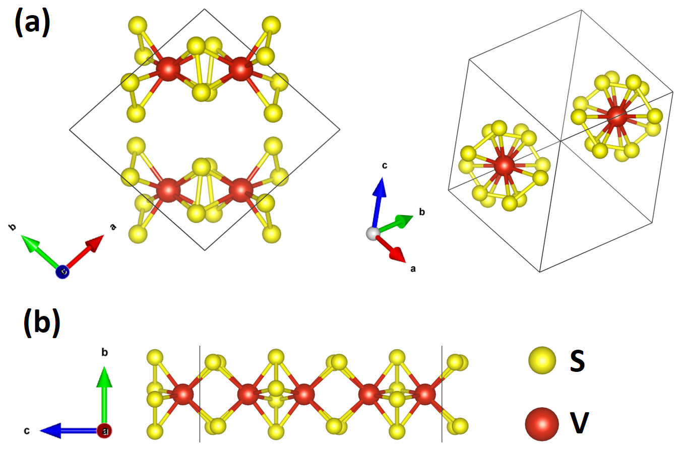
Figure 1a shows the primitive cell of \ceVS4 bulk phase (C2/c #15) in which each \ceV atom is coordinated with eight \ceS atoms forming four dimers. From the bulk phase, we have built the isolated NW unite cell (Figure 1b). The geometric data on the \ceVS4 bulk phase and on the isolated \ceVS4 NW are summarised in Table 1. Both the bulk and isolate NW phases of \ceVS4 are dynamically stable, as shown by the absence of an imaginary frequency in the phonon dispersion (figure S3a). The stability of these materials is also confirmed by AIMD simulation at room temperature, thus suggesting that individual NWs can be isolated (figure S3b).
| configurations | \ceE_form | \ceL_S-dimer | \ceL_V-V | \ceL_V-S | \ceE_g | \ceE_ex | \ce_B |
|---|---|---|---|---|---|---|---|
| Bulk | -2.59 | 2.03 | 2.77, 3.20 | 2.54, 2.39 | 2.24 | 0.961 | 1.15 |
| NW | -2.06 | 2.03 | 2.77, 3.22 | 2.55, 2.39 | 2.65 | 0.948 | 1.17 |
3.2 Electronic and magnetic properties
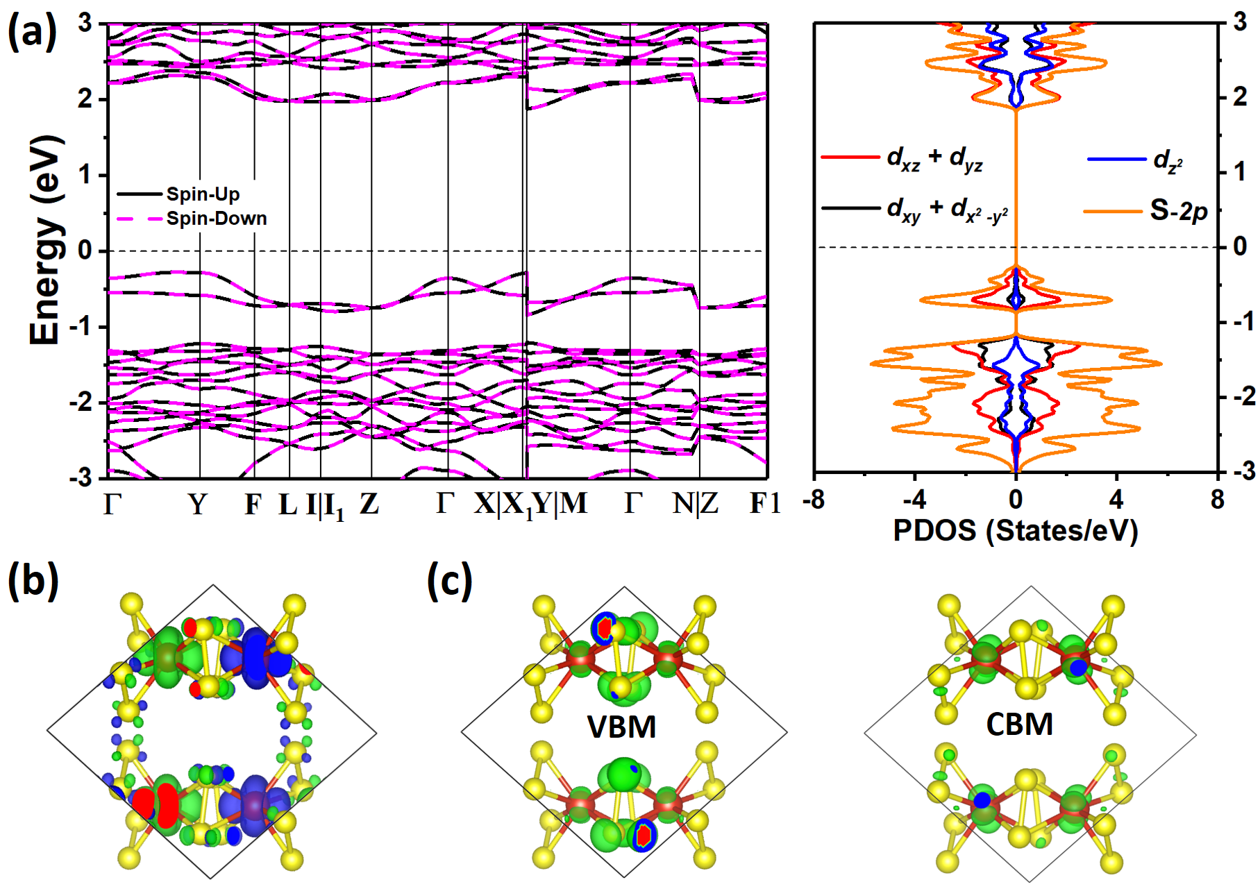
We now focus on the electronic and magnetic properties of the \ceVS4 bulk phase and the isolated NW. Both the bulk phase and the isolated NW have an AFM ground state, and their stability is given by \ceE_ex, as outlined in Table 1. The magnetic momentum of \ceV is similar in the bulk phase and in the isolated NW, with values of 1.15 and 1.17 \ce_B, respectively. The bulk phase has an indirect band gap of 2.24 \ceeV between the \ceY and \ceZ points of the Brillouin Zone. The calculated electronic band gap largely overestimated the experimental optical band gap of \ceVS4 films (approximately 1.35 \ceeV)45 which is usually observed in similar cases65, 66, 67. This difference of band gaps could be attributed to the experimental conditions in which the optoelectronic properties depend on the sulfur partial pressure of synthesis and on the morphology of the sample 45. Most importantly, our model for the bulk phase assumes perfect crystallinity, which is unlikely to occur in the family of low-dimensional compounds.
The spin density (Figure 2b) shows the AFM G-type motif of the material68. The valence band maximum (VBM) and the conduction band minimum (CBM) of the \ceVS4 bulk phase are formed by the overlap of \ceS 2 orbitals with \ceV levels as shown in the partial density of states (PDOS) (Figure 2a). The \ceV orbitals split into a non-degenerate orbital and into two 2-fold degenerate and orbitals. The local \ceV orbitals can induce an antiparallel spin arrangement on neighboring \ceV via the double-exchange mechanism (Figure 2b). The VBM and CBM of the \ceVS4 bulk phase derive from the \ceS 2 orbitals and \ceV orbitals (Figure 2c), in line with its PDOS.
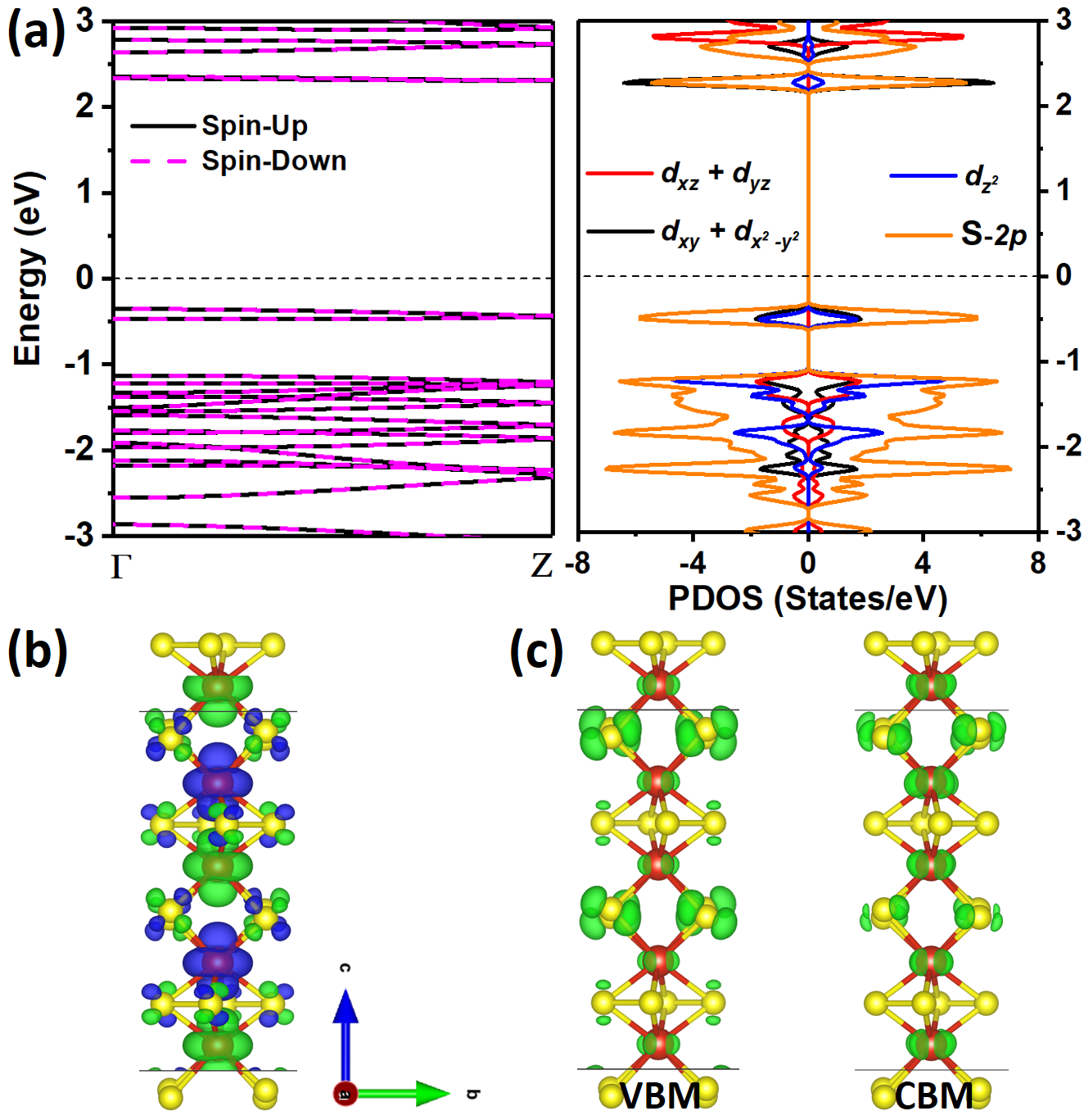
The electronic structure of the isolated \ceVS4 NW reflects the lower dimensionality of the material, which induces a larger band-gap of 2.65 \ceeV with a higher density of state (Figure 3a). The lack of interactions between different chains of \ceVS4 affects the nature of the bond. We can observe a larger contribution of VBM and CBM in the isolated \ceVS4 NW due to the \ceS 2 states (Figure 3a). The VBM and the CBM of the \ceV orbitals of the isolated NW are different from those of the bulk phase. \ceV orbitals of the isolated \ceVS4 NW contribute to the VBM and CBM.
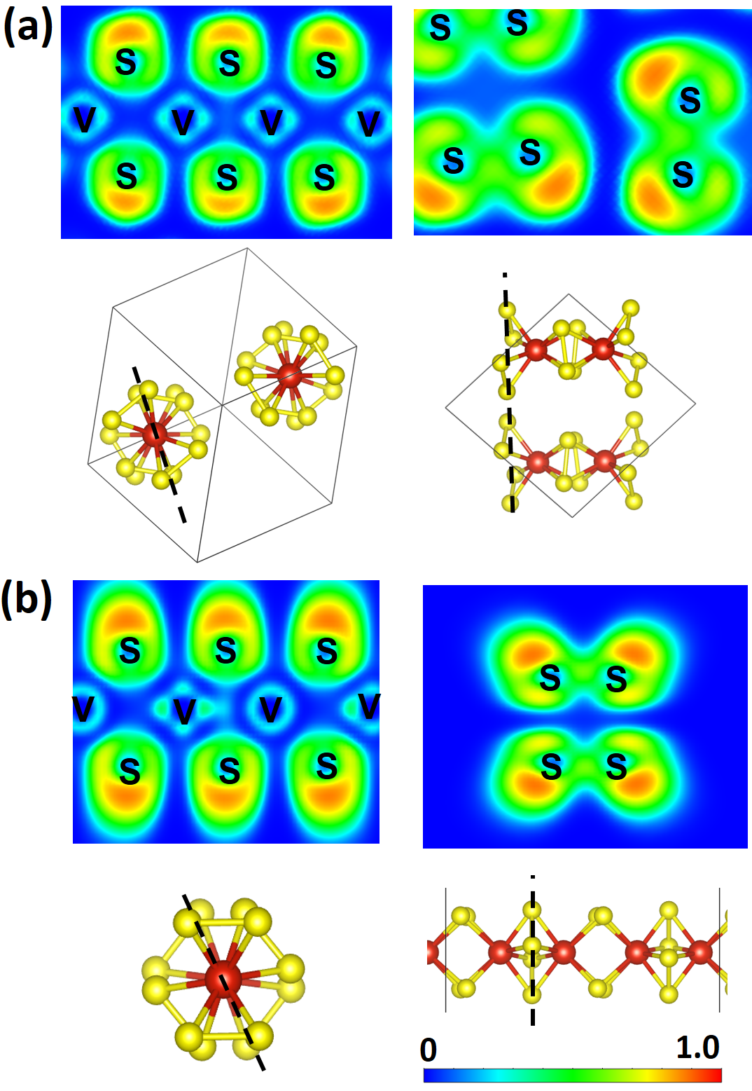
To further understand the change of electronic and magnetic properties between the \ceVS4 bulk phase and the isolated \ceVS4 NW, we plotted the electron localisation function (ELF) for the \ceVS4 bulk phase and for the isolated \ceVS4 NW (Figure 4). The ELF of \ceS atoms in the \ceVS4 bulk phase is more localised than that of the isolated \ceVS4 NW due to Van der Waals interactions of NWs in the \ceVS4 bulk phase. Moreover, \ceVS4 NW has distinct characteristics of localised electrons of \ceV atoms: more relatively itinerant \ceV electrons in the isolated \ceVS4 NW than that in the \ceVS4 bulk phase. Itinerant electrons of \ceV atoms can induce spin polarisation of neighbouring \ceS atoms, , an anti-parallel spin arrangement via a double-exchange mechanism. While the PDOS of orbitals of \ceV atoms differ between the \ceVS4 bulk phase and the isolated \ceVS4 NW. This difference in electronic properties does not affect the AFM character of these materials with a double-exchange mechanism, which also depends on the \ceV atoms.
3.3 Macroscopic magnetic properties
Magnetic order is more susceptible to temperature in materials with lower dimensionality69 due to the lower number of interactions. As a result, magnetic fluctuation, which destroys the order, is more likely to happen in low-dimensional materials than in three-dimensional materials. DFT calculations enable us to directly determine the magnitude of such interactions, but the value of \ceT_N cannot be simulated since it emerges as a statistic average. Nevertheless, we employed exchange interactions (obtained ab-initio) to describe the Temperature dependence of our system using an Ising model solved with a Monte Carlo approach. For the isolated \ceVS4 NW, we obtained a \ceT_N of 210 (Figure S4).
3.4 HMAF based FET
Previous studies have shown that carrier doping manipulates spin currents through the voltage gate34, 36. We analysed doping concentrations of 0.1, 0.3, and 0.5 electron (and hole) per unit cell of the isolated \ceVS4 NW (equivalent to 0.83, 2.50, and 4.17 ). The isolated \ceVS4 NW with carrier doping is HMAF, exhibiting complete spin-polarisation around the Fermi level (Figure 5). Because carrier doping shifts the Fermi level and spin polarisation of \ceS and \ceV atoms, PDOS for the isolated \ceVS4 NW with carrier doping show metallic states in the spin-up channel and semiconductor states (band gaps are over 2 .) in the spin-down channel. These effects are detected as small perturbations of the small AFM, which can be considered preserved for practical applications. The main contributions to the metallic states around the Fermi level derive from \ceV orbitals and \ceS 2 orbitals.
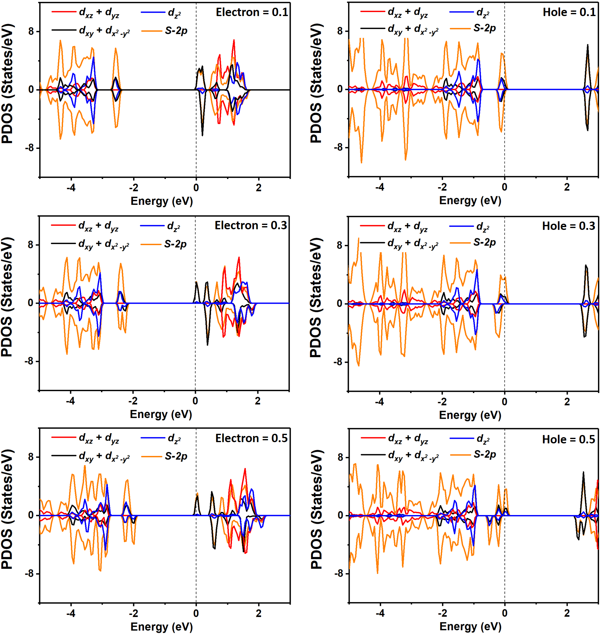
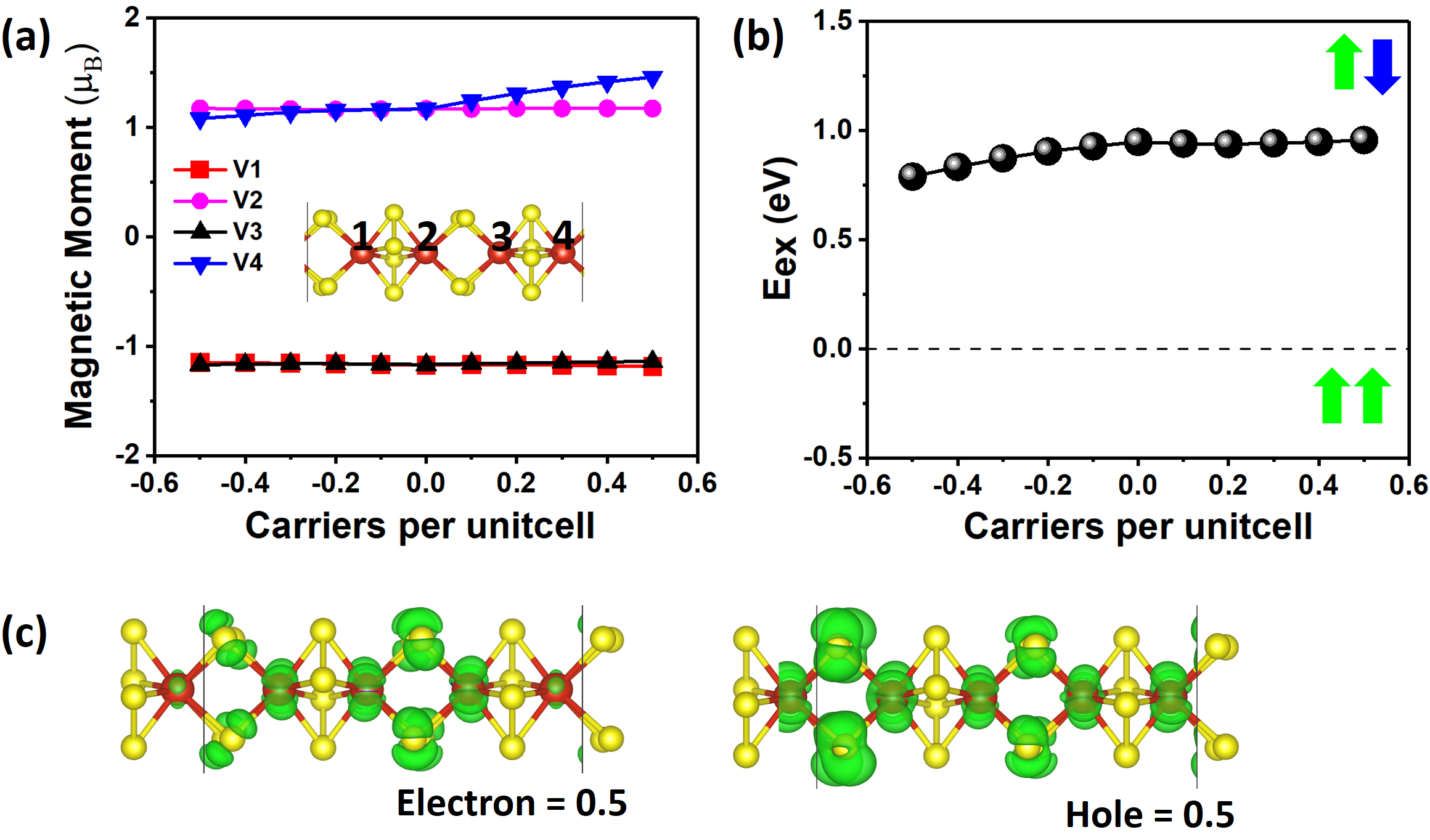
The magnetic momentum of \ceV atoms is affected by carrier doping, and the magnetic momentum of each \ceS atom is very small. When doping with 0.5 electron, the magnetic momentum of one \ceV atom (marked 4) increases from 1.17 to 1.46 \ce_B (Figure 6a). When doping with 0.5 hole, the magnetic momentum of one \ceV atom decreases from 1.17 to 1.08 \ce_B (Figure 6a). The isolated \ceVS4 NW retains its AFM state. The \ceE_ex is rapidly decreased under hole doping and increased under electron doping. Our results indicate that the AFM state of the isolated \ceVS4 NW is stable when injected with a low concentration of carriers. Moreover, we visualise the partial charge density (around Fermi level) of the isolated \ceVS4 NW at 0.5 electron and hole doping (Figure 6c). The participation of \ceV and \ceS orbitals also differs: formed by \ceV and \ceS 2 orbitals at 0.5 electron doping and by \ceV , and more \ceS 2 orbitals at 0.5 hole doping.
4 Discussion
Our results indicate that the isolated \ceVS4 NW is an AFM semiconductor with a high \ceT_N of 210 . This is an important result because ferromagnetic 1D materials, such as the quasi-1D organic ferromagnet (\ceT_C 0.56 )70, the tribromide NW of the half-metal \ceVBr3 (\ceT_C 80 )41, the trihydride molecular NW of the half-metal \ceCoH3 (\ceT_C 98 )38 and transition metal dihalide nanowires \ceCuCl2 (\ceT_C 14 )71, usually have much lower Curie temperatures (\ceT_C). Furthermore, \ceT_N of the isolated \ceVS4 NW is well above the temperature of liquid nitrogen (77K) and is also higher than that of different 2D antiferromagnets, such as bilayer \ceCrI3 (\ceT_N 45)72 or polyradical nanosheets (42.5)73. An even better prediction \ceT_N could be obtained for the isolated \ceVS4 NW, but this predriction is a promising starting point for further experimental characterisation.
Moreover, the AFM character and large band gap of the isolated NWs prevent spin-polarised currents in \ceVS4. The local spin polarisation of ideal antiferromagnetism, which in turn allows spin-polarised currents, could be a technological solution36. Here, we consider a model where carriers are injected into our materials, a process commonly know as carrier doping in the literature, in analogy to chemical doping74. A method for carrier doping consists of building a spin FET device (scheme shown in Figure S5) where the charges are injected by applying different gate voltages.
The influence of the environment on the transport properties and electrical contacts of NWs limit their applications. Therefore, protecting NWs by preserving the electronic and magnetic properties of the isolated \ceVS4 NW should be tested in spintronic applications. Nanotubes may protect NWs by preventing oxidation and maintaining electronic and magnetic properties unchanged37, 41, and nanocables, composed of insulating outer sheaths and a NW core, may guide the design of the models. Here, a designed nanocable on the isolated \ceVS4 NW and a (8, 8) boron nitride (BN) zigzag nanotube is constructed (Figure S6), where the lattice mismatch is approximately 4.5%. The isolated \ceVS4 NW has a slight strain. The distance between the NW and the wall of the BN nanotube is approximately 3.57 Å. The electronic and magnetic properties of the \ceVS4-BN nanocable is similar to that of the isolated \ceVS4 NW. Therefore, the spin polarisation of the nanocable mainly derives from the inner NW, while the outer nanotube has a negligible effect on the nanocable. Such a hybrid structure may also enable interesting applications in spintronics.
5 Summary
We presented herein a new strategy in \ceVS4 NWs towards AFM spintronics. The \ceVS4 NWs are bound together by Van der Waals forces to form nano-rods in quasi-1D compounds in experiments. In this context, the geometric, electronic and magnetic properties of the \ceVS4 bulk phase and isolated \ceVS4 NW were analysed. First, we investigated the stability of the \ceVS4 bulk phase and isolate \ceVS4 NW by formation energy, AIMD and phonon spectra. After confirming the stability of \ceVS4 NWs, we investigated the electronic and magnetic properties of \ceVS4 NWs. The magnetic ground states of the isolate \ceVS4 NW is AFM with a high Néel temperature (210 ). Detecting and manipulating the spin of AFM materials remains a major challenge due to spin degeneracy in the band structure. Nevertheless, carrier doping can separate the spin degeneracy to induce local spin polarisation. The isolated \ceVS4 NW represent the half-metallic antiferromagnet resulting from carrier doping, which can be achieved with gate voltages. Our results indicate that the isolated \ceVS4 NW is a promising 1D material for AFM spintronic applications. Carrier doping induces a rigid shift in the Fermi level into the valence or conduction bands, resulting in a complete spin-polarisation of carriers, which can be induced by applying a gate voltage. Thus, spin polarisation currents can be manipulated by applying a gate voltage, with a high potential for spintronic applications. We further considered the protection of NWs. BN nanotubes can provide protection by preventing oxidation and by preserving the electronic and magnetic properties of \ceVS4 NWs. Our results open up new oppportunities for applying 1D NWs in AFM spintronics by inducing half-metallic antiferromagnetism.
6 Conflicts of interest
There are no conflicts to declare.
7 Acknowledgements
Charles University Centre of Advanced Materials (CUCAM) (OP VVV Excellent Research Teams, Project No. CZ.02.1.01/0.0/0.0/15 _003/0000417) is acknowledged. S. L. acknowledges the support from GAUK project (Grant No. 792218). The results from this research have been achieved using the DECI resource Kay based in Poblacht na hÉireann at ICHEC with support from the PRACE DECI-16 16DECI0034 CABLE project. We also acknowledge the computer resources, technical expertise, and assistance provided by IT4Innovations National Supercomputing Center. We thank Carlos V. Melo Carlos for editing the manuscript.
Notes and references
- Del Alamo 2011 J. A. Del Alamo, Nature, 2011, 479, 317.
- Tomioka et al. 2012 K. Tomioka, M. Yoshimura and T. Fukui, Nature, 2012, 488, 189.
- Ferain et al. 2011 I. Ferain, C. A. Colinge and J.-P. Colinge, Nature, 2011, 479, 310.
- Mack 2011 C. A. Mack, IEEE Transactions on Semiconductor Manufacturing, 2011, 24, 202–207.
- Lu and Lieber 2010 W. Lu and C. M. Lieber, Nanoscience And Technology: A Collection of Reviews from Nature Journals, World Scientific, 2010, pp. 137–146.
- Akinwande et al. 2014 D. Akinwande, N. Petrone and J. Hone, Nature Communications, 2014, 5, 5678.
- Berger et al. 2004 C. Berger, Z. Song, T. Li, X. Li, A. Y. Ogbazghi, R. Feng, Z. Dai, A. N. Marchenkov, E. H. Conrad, P. N. First et al., The Journal of Physical Chemistry B, 2004, 108, 19912–19916.
- Wolf et al. 2001 S. Wolf, D. Awschalom, R. Buhrman, J. Daughton, S. Von Molnar, M. Roukes, A. Y. Chtchelkanova and D. Treger, science, 2001, 294, 1488–1495.
- Felser et al. 2007 C. Felser, G. H. Fecher and B. Balke, Angewandte Chemie International Edition, 2007, 46, 668–699.
- Li and Yang 2016 X. Li and J. Yang, National Science Review, 2016, 3, 365–381.
- Schaibley et al. 2016 J. R. Schaibley, H. Yu, G. Clark, P. Rivera, J. S. Ross, K. L. Seyler, W. Yao and X. Xu, Nature Reviews Materials, 2016, 1, 16055.
- Zhong 2017 D. Zhong, Science Advances, 2017, 3, e1603113.
- Jungwirth et al. 2018 T. Jungwirth, J. Sinova, A. Manchon, X. Marti, J. Wunderlich and C. Felser, Nature Physics, 2018, 14, 200–203.
- Žutić et al. 2004 I. Žutić, J. Fabian and S. D. Sarma, Reviews of Modern Physics, 2004, 76, 323.
- Chumak et al. 2015 A. V. Chumak, V. I. Vasyuchka, A. A. Serga and B. Hillebrands, Nature Physics, 2015, 11, 453–461.
- Camsari et al. 2015 K. Y. Camsari, S. Ganguly and S. Datta, Scientific reports, 2015, 5, 10571.
- Mott 1936 N. F. Mott, Proceedings of the Royal Society of London. Series A-Mathematical and Physical Sciences, 1936, 156, 368–382.
- Picozzi 2014 S. Picozzi, Frontiers in Physics, 2014, 2, 10.
- Mott 1936 N. F. Mott, Proceedings of the Royal Society of London. Series A-Mathematical and Physical Sciences, 1936, 153, 699–717.
- Li and Yang 2017 X. Li and J. Yang, Wiley Interdisciplinary Reviews: Computational Molecular Science, 2017, 7, e1314.
- Jungwirth et al. 2016 T. Jungwirth, X. Marti, P. Wadley and J. Wunderlich, Nature Nanotechnology, 2016, 11, 231.
- Baltz et al. 2018 V. Baltz, A. Manchon, M. Tsoi, T. Moriyama, T. Ono and Y. Tserkovnyak, Reviews of Modern Physics, 2018, 90, 015005.
- MacDonald and Tsoi 2011 A. H. MacDonald and M. Tsoi, Philosophical Transactions of the Royal Society A: Mathematical, Physical and Engineering Sciences, 2011, 369, 3098–3114.
- Hu 2012 X. Hu, Advanced Materials, 2012, 24, 294–298.
- He et al. 2015 J. He, P. Zhou, N. Jiao, X. Chen, W. Lu and L. Sun, RSC Advances, 2015, 5, 46640–46647.
- Nie and Hu 2008 Y.-m. Nie and X. Hu, Physical Review Letters, 2008, 100, 117203.
- Van Leuken and De Groot 1995 H. Van Leuken and R. De Groot, Physical Review Letters, 1995, 74, 1171.
- Nayak et al. 2015 A. K. Nayak, M. Nicklas, S. Chadov, P. Khuntia, C. Shekhar, A. Kalache, M. Baenitz, Y. Skourski, V. K. Guduru, A. Puri et al., Nature Materials, 2015, 14, 679.
- Kurt et al. 2014 H. Kurt, K. Rode, P. Stamenov, M. Venkatesan, Y.-C. Lau, E. Fonda and J. Coey, Physical Review Letters, 2014, 112, 027201.
- Gong et al. 2018 S.-J. Gong, C. Gong, Y.-Y. Sun, W.-Y. Tong, C.-G. Duan, J.-H. Chu and X. Zhang, Proceedings of the National Academy of Sciences, 2018, 115, 8511–8516.
- Ai et al. 2018 H. Ai, X. Liu, B. Yang, X. Zhang and M. Zhao, The Journal of Physical Chemistry C, 2018, 122, 1846–1851.
- Chuang et al. 2015 P. Chuang, S.-C. Ho, L. W. Smith, F. Sfigakis, M. Pepper, C.-H. Chen, J.-C. Fan, J. Griffiths, I. Farrer, H. E. Beere et al., Nature Nanotechnology, 2015, 10, 35–39.
- Deng et al. 2018 Y. Deng, Y. Yu, Y. Song, J. Zhang, N. Z. Wang, Z. Sun, Y. Yi, Y. Z. Wu, S. Wu, J. Zhu et al., Nature, 2018, 563, 94–99.
- Li et al. 2014 X. Li, X. Wu and J. Yang, Journal of the American Chemical Society, 2014, 136, 11065–11069.
- Yuan et al. 2009 H. Yuan, H. Shimotani, A. Tsukazaki, A. Ohtomo, M. Kawasaki and Y. Iwasa, Advanced Functional Materials, 2009, 19, 1046–1053.
- He et al. 2019 J. He, G. Ding, C. Zhong, S. Li, D. Li and G. Zhang, Nanoscale, 2019, 11, 356–364.
- Pham et al. 2018 T. Pham, S. Oh, P. Stetz, S. Onishi, C. Kisielowski, M. L. Cohen and A. Zettl, Science, 2018, 361, 263–266.
- Li et al. 2017 X. Li, H. Lv, J. Dai, L. Ma, X. C. Zeng, X. Wu and J. Yang, Journal of the American Chemical Society, 2017, 139, 6290–6293.
- Wan et al. 2018 Y. Wan, Y. Sun, X. Wu and J. Yang, The Journal of Physical Chemistry C, 2018, 122, 989–994.
- Zhang et al. 2016 T. Zhang, L. Zhu and G. Chen, Journal of Materials Chemistry C, 2016, 4, 10209–10214.
- Li et al. 2018 S.-s. Li, Y.-p. Wang, S.-j. Hu, D. Chen, C.-w. Zhang and S.-s. Yan, Nanoscale, 2018, 10, 15545–15552.
- Ye et al. 2017 H. Ye, L. Wang, S. Deng, X. Zeng, K. Nie, P. N. Duchesne, B. Wang, S. Liu, J. Zhou, F. Zhao et al., Advanced Energy Materials, 2017, 7, 1601602.
- Shang et al. 2020 C. Shang, L. Fu, S. Zhou and J. Zhao, JACS Au, 2020, https://doi.org/10.1021/jacsau.0c00049.
- Hillebrand 1907 W. Hillebrand, Journal of the American Chemical Society, 1907, 29, 1019–1029.
- Flores et al. 2018 E. Flores, E. Munoz-Cortes, J. Bodega, O. Caballero-Calero, M. Martin-Gonzaalez, C. Sanchez, J. R. Ares and I. J. Ferrer, ACS Applied Energy Materials, 2018, 1, 2333–2340.
- Zhou et al. 2016 Y. Zhou, Y. Li, J. Yang, J. Tian, H. Xu, J. Yang and W. Fan, ACS Applied Materials & Interfaces, 2016, 8, 18797–18805.
- Lui et al. 2015 G. Lui, G. Jiang, A. Duan, J. Broughton, J. Zhang, M. W. Fowler and A. Yu, Industrial & Engineering Chemistry Research, 2015, 54, 2682–2689.
- Rout et al. 2013 C. S. Rout, B.-H. Kim, X. Xu, J. Yang, H. Y. Jeong, D. Odkhuu, N. Park, J. Cho and H. S. Shin, Journal of the American Chemical Society, 2013, 135, 8720–8725.
- Sun et al. 2015 R. Sun, Q. Wei, Q. Li, W. Luo, Q. An, J. Sheng, D. Wang, W. Chen and L. Mai, ACS Applied Materials & Interfaces, 2015, 7, 20902–20908.
- Wang et al. 2018 S. Wang, F. Gong, S. Yang, J. Liao, M. Wu, Z. Xu, C. Chen, X. Yang, F. Zhao, B. Wang et al., Advanced Functional Materials, 2018, 28, 1801806.
- Wang et al. 2018 Y. Wang, Z. Liu, C. Wang, X. Yi, R. Chen, L. Ma, Y. Hu, G. Zhu, T. Chen, Z. Tie et al., Advanced Materials, 2018, 30, 1802563.
- Gao et al. 2016 G. Gao, G. Ding, J. Li, K. Yao, M. Wu and M. Qian, Nanoscale, 2016, 8, 8986–8994.
- Frey et al. 2019 N. C. Frey, A. Bandyopadhyay, H. Kumar, B. Anasori, Y. Gogotsi and V. B. Shenoy, ACS nano, 2019, 13, 2831–2839.
- Ma et al. 2017 Y. Ma, A. Kuc, Y. Jing, P. Philipsen and T. Heine, Angewandte Chemie International Edition, 2017, 56, 10214–10218.
- Kresse 1993 G. Kresse, Physical Review B, 1993, 47, 558.
- Kresse 1999 G. Kresse, Physical Review B, 1999, 59, 1758.
- Perdew et al. 1996 J. P. Perdew, K. Burke and M. Ernzerhof, Physical Review Letters, 1996, 77, 3865.
- Heyd et al. 2003 J. Heyd, G. E. Scuseria and M. Ernzerhof, The Journal of Chemical Physics, 2003, 118, 8207–8215.
- Grimme et al. 2010 S. Grimme, J. Antony, S. Ehrlich and H. Krieg, The Journal of Chemical Physics, 2010, 132, 154104.
- Togo and Tanaka 2015 A. Togo and I. Tanaka, Scr. Mater., 2015, 108, 1–5.
- Nosé 1984 S. Nosé, The Journal of Chemical Physics, 1984, 81, 511–519.
- Watanabe 1974 Y. Watanabe, Acta Crystallographica Section B: Structural Crystallography and Crystal Chemistry, 1974, 30, 1396–1401.
- McCoy and Wu 2014 B. M. McCoy and T. T. Wu, The two-dimensional Ising model, Courier Corporation, 2014.
- Albuquerque et al. 2007 A. F. Albuquerque, F. Alet, P. Corboz, P. Dayal, A. Feiguin, S. Fuchs, L. Gamper, E. Gull, S. Gürtler, A. Honecker et al., Journal of Magnetism and Magnetic Materials, 2007, 310, 1187–1193.
- Zhou et al. 2018 T. Zhou, Z. Zang, J. Wei, J. Zheng, J. Hao, F. Ling, X. Tang, L. Fang and M. Zhou, Nano Energy, 2018, 50, 118 – 125.
- Ur Rehman et al. 2017 S. Ur Rehman, Z. Li, H. Li and Z. Ding, Physica B: Condensed Matter, 2017, 524, 163 – 172.
- Lou and Lee 2019 P. Lou and J. Y. Lee, The Journal of Chemical Physics, 2019, 150, 184307.
- Hotta et al. 1999 T. Hotta, S. Yunoki, M. Mayr and E. Dagotto, Physical Review B, 1999, 60, 15009–15012.
- Gambardella 2008 P. Gambardella, Magnetic Nanostructures in Modern Technology, Dordrecht, 2008, pp. 325–342.
- Takahashi et al. 1991 M. Takahashi, P. Turek, Y. Nakazawa, M. Tamura, K. Nozawa, D. Shiomi, M. Ishikawa and M. Kinoshita, Physical Review Letters, 1991, 67, 746.
- Tan et al. 2020 X. Tan, L. Liu, H. Xiang, G.-F. Du, A. Lou and H.-H. Fu, Nanoscale, 2020, 12, 8942–8948.
- Huang et al. 2018 B. Huang, G. Clark, D. R. Klein, D. MacNeill, E. Navarro-Moratalla, K. L. Seyler, N. Wilson, M. A. McGuire, D. H. Cobden, D. Xiao et al., Nature Nanotechnology, 2018, 13, 544–548.
- Yang et al. 2018 Y. Yang, C. Liu, X. Xu, Z. Meng, W. Tong, Z. Ma, C. Zhou, Y. Sun and Z. Sheng, Polymer Chemistry, 2018, 9, 5499–5503.
- Ueno et al. 2011 K. Ueno, S. Nakamura, H. Shimotani, H. Yuan, N. Kimura, T. Nojima, H. Aoki, Y. Iwasa and M. Kawasaki, Nature Nanotechnology, 2011, 6, 408.