Spatially mapping the thermal conductivity of graphene by an opto-thermal method
Abstract
Mapping the thermal transport properties of materials at the nanoscale is of critical importance for optimizing heat conduction in nanoscale devices. Several methods to determine the thermal conductivity of materials have been developed, most of them yielding an average value across the sample, thereby disregarding the role of local variations. Here, we present a method for the spatially-resolved assessment of the thermal conductivity of suspended graphene by using a combination of confocal Raman thermometry and a finite-element calculations-based fitting procedure. We demonstrate the working principle of our method by extracting the two-dimensional thermal conductivity map of one pristine suspended single-layer graphene sheet and one irradiated using helium ions. Our method paves the way for spatially resolving the thermal conductivity of other types of layered materials. This is particularly relevant for the design and engineering of nanoscale thermal circuits (e.g. thermal diodes).
keywords:
American Chemical Society, LaTeX[Basel University] Department of Physics, University of Basel, Klingelbergstrasse 82, CH-4056 Basel, Switzerland \altaffiliationCurrent address: Department of Mechanical and Process Engineering, ETH Zurich, Tannenstrasse 3, CH-8092 Zurich, Switzerland Basel University] Department of Physics, University of Basel, Klingelbergstrasse 82, CH-4056 Basel, Switzerland \alsoaffiliation[Basel University] Department of Physics, University of Basel, Klingelbergstrasse 82, CH-4056 Basel, Switzerland \alsoaffiliation[SNI] Swiss Nanoscience Institute, University of Basel, Klingelbergstrasse 82, CH-4056 Basel, Switzerland \abbreviationsIR,NMR,UV
Keywords: graphene, thermal conductivity, Raman spectroscopy, two-dimensional mapping, suspended
![[Uncaptioned image]](/html/2101.12238/assets/x1.png)
1 Introduction
Thermal properties of materials are of crucial importance for optimizing heat management in nanoscale devices, with the thermal conductivity as key material property.1, 2 The thermal conductivity is typically determined by monitoring the sample temperature and/or heat flow in response to a local heat source, in combination with an analytical expression or a numerical model. For instance, for bulk materials, the well-known 3 technique3, 4 is used, while for nanoscale materials, methods such as the thermal bridge method 5, 6, 7 and micro-Raman spectroscopy8, 9, 10, 11 provide the thermal conductivity of the material.
Of particular interest are the thermal properties of layered materials. Due to their broad range of conductivity values and their atomically thin nature, such materials are highly relevant for heat management at the nanoscale.12, 13 One of the most appealing materials is graphene, with extraordinarily high thermal conductivity values. However, extracting the thermal properties of 2D materials is challenging, in particular when suspended to reduce the influence of the substrate. For example, time-domain thermoreflectance cannot be applied to 2D materials as the material is too thin14. Scanning thermal probe microscopy, on the other hand, despite possessing nanometer resolution, is highly delicate to perform on suspended 2D materials. Moreover, both techniques rely on on-chip heaters for channeling heat into the system. Raman spectroscopy can overcome these difficulties, as it can utilize the excitation laser to locally heat the device, while at the same time measuring the local temperature. Moreover, Raman spectroscopy can be conveniently performed on suspended graphene films for eliminating the influence of the substrate. Using Raman spectroscopy, Balandin and Ghosh et al.15, 16 determined the thermal conductivity of suspended graphene to be as high as 5000 Wm-1K-1 at room temperature. Their opto-thermal method, measuring the shift of the Raman G-band upon laser irradiation for estimating the local temperature, has been extensively used in literature since. Alternatives based on the intensity ratio of Stokes to anti-Stokes Raman scattering17 or the Raman 2D-band18 have also been reported.
Using this opto-thermal method, the influence of the quality and structure of the graphene, as well as the environment have been extensively investigated. For instance, Cai et al.19 reported values for exceeding 2500 Wm-1K-1 for suspended graphene grown by chemical vapor deposition (CVD), and Chen et al.20 studied the influence of environment on thermal conductivity of graphene. Isotopically pure 12C (0.01 13C) graphene has been shown to exhibit = 4000 Wm-1K-1, a factor of two higher than in graphene composed of a 1:1 mixture of 12C and 13C.21 Also, the influence of CVD-graphene’s polycrystallinity on the thermal conductivity was studied by Lee et al. and Ma et al., revealing that smaller grain sizes drastically reduce due to grain boundary scattering.22, 23 Along similar lines, wrinkles24, oxygen-plasma induced defects25, and electron beam irradiation26 have shown to reduce the thermal conductivity.
In all the above-mentioned studies, the one-dimensional heat equation is used to fit the experimental temperature and extract the thermal conductivity. However, such approaches yield an average value of thermal conductivity value, not a spatially resolved map. This implied that local variations caused by defects, folds, contaminants, etc. are neglected.
For going beyond the average material property value, approaches mapping the temperature distribution in the sample are necessary, combined with multi-dimensional analytical of numerical model. A range of techniques has been developed for nanoscale thermometry, such as time-domain thermoreflectance27, Raman spectroscopy15, 16, scanning thermal probe microscopy28, 29, 30, polymer imprint thermal mapping31 and electron energy loss spectroscopy32, providing means to locally map the sample temperature.
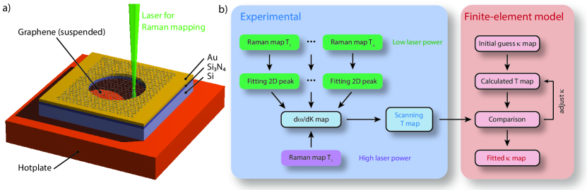
Here, we introduce an opto-thermal method that allows for two-dimensional mapping of thermal conductivity of suspended graphene membranes. The presented method relies on a combination of scanning -Raman spectroscopy with finite-element method (FEM) calculations. The workflow for our approach is presented in Figure. 1. In the first experimental stage, a series of two-dimensional Raman spectroscopy maps are used to construct a temperature map of the membrane upon illumination. More specifically, Raman maps are recorded for various hotplate temperatures and at a low laser power. This series of maps is used to construct a calibration map of the Raman peak shifts with temperature. Then, another Raman map is recorded at high-laser-power, which, combined with the calibration map, is used to construct a temperature map of the membrane upon laser heating.
The constructed experimental temperature map is then used as an input for the FEM-based fit procedure. For a given initial guess of the thermal conductivity, the lattice temperature upon laser illumination is calculated. The thermal conductivity is then iteratively adjusted, until the computed temperature map matches the experimental one. We apply this fit procedure to extract the thermal conductivity of a pristine graphene membrane that is suspended over a silicon nitride frame. Finally, we demonstrate that the thermal conductivity of the graphene membrane can be tuned in a controlled way by the introduction of helium-ion (He+-ion) induced defects in the membrane.
2 Results
2.1 Experimental temperature maps
The CVD-graphene membranes are prepared as described in section 1 of the Supporting Information and previously. 33, 34, 35, 36. We applied Raman spectroscopy to obtain the lattice temperature of the suspended graphene membranes (for details see section 2 of the Supporting Information). Here, we focus on the 2D-band due to its high sensitivity to temperature changes22, 20 of around -0.07 cm-1/K. Alternatively, one can also rely on the G-peak due to its high linearity in peak shift versus temperature.16, 19, 37.
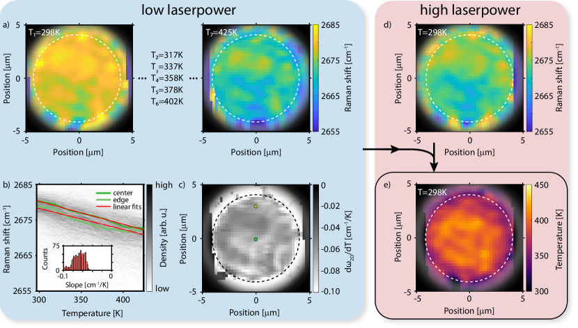
Figure 2a) presents maps of the Lorentzian-fitted 2D-peaks acquired at temperatures T1-T7 ranging between 298 K and 425 K. The Raman spectra have been acquired at low laser power (0.25 mW) to limit any heating effects using a 532 nm excitation laser (for details see section 4 and 5 of the Supporting Information). For each pixel, the peak shift with hot plate temperature () is fitted using a first-order polynomial, as shown in Figure 2b). The inset presents a histogram of the slopes, showing a Gaussian distribution centered around -0.07 cm-1/K. The spatial distribution of the peak shifts with temperature is displayed in Figure 2c), showing substantial spatial variations. Once this calibration map is acquired, a Raman map of the graphene membrane is acquired at high laser power (4 mW), as shown in Figure 2d). The high laser power causes the graphene to locally heat, resulting in a shift in the Raman peak position. By combining this high-power measurement with the map obtained at low laser power, a map of the average temperature within the laser spot is obtained for each laser position, as shown in Figure 2b). We note that local variations in the temperature upon illumination on the order of 50-100 K are observed, highlighting the importance of spatially mapping the temperature, superior to other techniques that extract thermal conductivity from a single spot.
2.2 FEM calculations
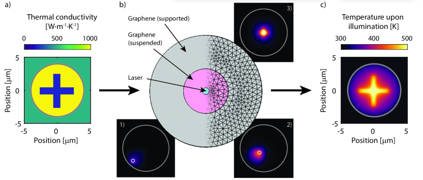
FEM calculations are employed for the computation of the temperature map of the system upon laser illumination for a given spatial thermal conductivity distribution. This concept is illustrated in Figure 3. As an input, a two-dimensional map of the thermal conductivity is provided, of which an example is shown Figure 3a). Figure 3b) presents the layout of the system (not to scale). A detailed description of the FEM calculation and the implementation thereof is provided in section S3 of the Supporting Information. While scanning the laser across the membrane, the full temperature distribution is calculated for each laser spot position on the membrane (three examples are provided in Figure 3b).
For each of these temperature distributions, the average temperature within the laser spot is calculated, from which all values are combined to obtain a two-dimensional map of the graphene temperature upon illumination. This induced-temperature map is presented in Figure 3c) and represents the same temperature map that is obtained experimentally upon illumination of the sample with high laser power.
To obtain the thermal conductivity map, an iterative minimization procedure is employed. More information can be found in section S3 of the Supporting Information, in which we also validate the numerical method on a simulated system with a known thermal conductivity map. The starting point is an initial (typically uniform) guess of the thermal conductivity. In each iteration of the process, the corresponding induced temperature map is compared to the experimental temperature map, after which the thermal conductivity is adjusted pixel-wise according to the temperature difference. This process is repeated until convergence is reached.
2.3 Thermal conductivity map based on fitted experimental temperature map
The induced temperature map obtained in Figure 2 is used as input for the iterative procedure to obtain the thermal conductivity map. Here, as clarified in section 4 of the Supporting Information, we use a uniform absorption of 2.7 % for the suspended graphene and double that value (5.4 %) for the supported graphene. Moreover, all the employed model parameters are summarized in Table S1 of the SI. Importantly, in the model, a diffraction-limited spot size of 300 nm is assumed. Moreover, the thermal conductivity of graphene on the supporting part, the thermal coupling to the substrate, as well as the convection parameter are taken from literature19.
Finally, we note that it is challenging to model the transition from the suspended graphene to the supported graphene once the laser spot is in the vicinity of the edge due to 1.) reflection from of the laser excitation at the edges of the support may lead to an increase in the deposited laser power, 2.) quenching of the Raman scattered light on the substrate may lead to an overestimation of the local temperature as the 2D peak of the suspended graphene is more pronounced than that of the supported graphene.
To circumvent this issue, the thermal conductivity of the first 0.5 of the membranes away from the support are not fitted and kept at a fixed value. Finally, the thermal conductivity is fitted for 100 iterations, after which the absorption is fitted for the same number of cycles. More details about this procedure can be found in section 2 of the SI. For numerical stability reasons, we put a lower value on the thermal conductivity at 100 Wm-1K-1.
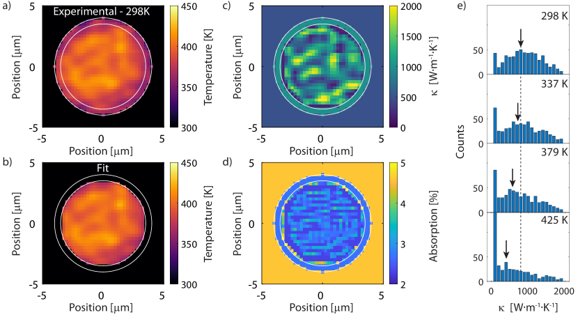
Figure 4a) presents the experimental temperature map, as obtained in Figure 2e), alongside the fitted temperature map in Figure 4b. The two maps closely resemble each other. The corresponding thermal conductivity map is presented in Figure 4c). We find that the local thermal conductivity values range from 500 to 2000 Wm-1K-1 with an average value of 1007450 Wm-1K-1 highlighting the importance of spatially resolving the thermal conductivity. The average value is in agreement with values reported previously as well as by other methods.38, 39 In Figure 4e), we present a histogram of the fitted thermal conductivity map for increasing hot plate temperatures. The bar plots show that for increasing temperature a gradual decrease in thermal conductivity is observed. This behavior follows the trend observed by others 20, 21, 22.
2.4 Thermal conductivity of defect-engineered graphene
As a final demonstration of the capability of the presented method, we study the thermal conductivity of a graphene membrane that is exposed to He+-ions using focused ion beam lithography. As shown previously, He+-ions can be used to induce, in a controlled fashion, defects in suspended graphene membranes and other two-dimensional materials35, 40.
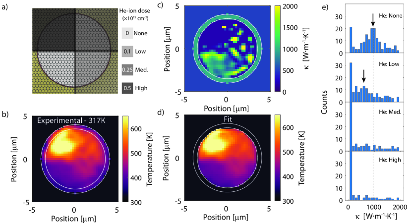
Figure 5a) presents the exposure pattern as well as the used irradiation doses. The membrane is divided into four quadrants, with the He+-ion irradiation steadily increasing in the counter-clockwise direction, starting in the lower left with no He+-ion dose. Manually selected representative Raman spectra of each quadrant are presented in Figure S10 of the Supporting Information, exhibiting all the characteristic graphene peaks. The selection of the representative Raman spectra can also be done by an advanced clustering approach to avoid any human bias as described elsewhere.41 Upon an increase of the He+-ion dose, the D-band intensity steadily increases. The intensity ratio of the D and D’ band I(D)/I(D’) upon irradiation, is indicative of the type of defect.42. We extract this ratio by fitting the ratios I(D)/I(G) versus I(D’)/I(G) for various He+-ion doses. We find an intensity ratio of 11.7 for the defect-engineered graphene. This value is comparable to the reported intensity ratio of 13 for sp3 type of defects (see section 6 of the Supporting Information). We employ the same procedure as presented in Figures 2 for the extraction of the temperature. Figure 5b) presents the induced temperature map upon a 4 mW laser illumination. In this plot, the four quadrants are visible, with the lowest temperatures recorded in the (unexposed) lower left section of the membrane, and the highest one in the upper left (most exposed). This temperature map is used as input for the iterative FEM-based fitting procedure, resulting in the fitted thermal conductivity map in Figure 5c) and the corresponding fitted temperature map shown in Figure 5d). Figure 5e) presents a histogram of the thermal conductivity of each of the four quadrants. A steady decrease in average conductivity is observed, from 1000 Wm-1K-1 for the no He+-ion irradiation, and 100 Wm-1K-1 for the highest He+-ion dose. This decrease in thermal conductivity with increasing defect density is in agreement with previous reports25, 26.
3 Discussion
The FEM calculations employed here assume that the heat transport through the system is following Fourier’s Law. This assumption implies that the phonon mean free path is much smaller than the membrane size. Indeed, ballistic phonon transport has been reported in several nanosystems at room temperature: In substrate-supported graphene the phonon mean free path is 100 nm43; for suspended graphene discs, the transition from ballistic to diffusive transport occurs at 775 nm44 while in ultra-thin nanowires phonon mean free paths of several micrometers have been observed45. Therefore, the resolution of the presented method is limited by the phonon mean free path as a spatial mapping of the thermal conductivity below this length scale would require a heat transport description based on the Boltzmann transport equation46, 47, 48. Given this boundary condition, the resolution of 250 nm used in this study is close to the ultimate resolution this FEM-based method allows.
A limitation of the presented method is the time consumption of the temperature calibration, reducing its use in high-throughput applications. As the laser power is low, acquiring the two-dimensional Raman map at each temperature requires several hours. This long acquisition time can also lead to a drift in the sample position during the measurement. To reduce this drift, clamping of the sample and a good thermalization of the sample with the environment is crucial. Furthermore, as changing the hot plate temperature leads to shifts of the sample position, the Raman maps acquired at various temperatures need to be aligned one versus the other.
A second limitation is the fixed value for the absorption of 2.7 % that is used for the first 100 cycles of the fitting procedure, after which the absorption is fitted as well. The accuracy of the model may be improved by experimentally determining the absorption at the various hot plate temperatures. Ideally, the absorption would be measured by simultaneously monitoring the transmitted, and reflected laser power while scanning across the sample. We stress that simultaneously measuring both components is crucial, as contaminations and residues on the membrane may scatter the laser light, leading to a reduction in the transmitted light, but not to an increase in absorption. However, such a measurement is challenging and technically unfeasible in our current setup.
Despite the previously mentioned limitations, our method is well suited for studying the thermal properties of two-dimensional materials, in particular for materials with an anisotropic thermal conductivity49, 50, 51. The method can also be extended to characterize van der Waals materials consisting of multiple layers. Furthermore, the method is extensible from two to three dimensions, allowing for modeling of more complex device geometries, including, for instance, stacks of 2D-materials, or the presence of contact electrodes of finite thickness. As such, it could be used for assessing the material quality after device integration. Also, as the individual two-dimensional materials in a stacked geometry each have a distinct Raman signature, it is possible to investigate the subsurface thermal properties of materials, such as, for instance, graphene embedded in a thin hexagonal boron nitride layer. Alternatively, when the material under study is on a substrate or thick enough, other means of determining the temperature map may be used, like time-domain thermoreflectance, for reduced measurement time and improve throughput.
4 Conclusion
We have introduced a method for spatially mapping the thermal conductivity of single-layer graphene using a combination of Raman spectroscopy and finite-element calculations at ultimate resolution. We anticipate that this method can be applied to other single- and few layer materials. We applied the method to obtain the thermal conductivity of a pristine and He+-ion patterned suspended single-layer graphene film. For the unpatterned film, large variations of the extracted thermal conductivity are observed and attributed to local irregularities such as contamination, defects, or folds. These findings highlight the importance of spatial mapping of the thermal conductivity, in contrast to measurement approaches that yield a thermal conductivity averaged across the entire sample. On the patterned membrane, we demonstrate controlled engineering of the thermal conductivity by He+-ion irradiation. As Raman spectroscopy is widely used in the two-dimensional materials community, our method is ideally suited for studying the thermal properties of other layered materials. Moreover, the working principle of the FEM method can easily be extended to more complex geometries or interfaces, in particular combined with alternative measurement techniques for providing a temperature map. Our method enables spatially resolving the thermal conductivity of atomically thin materials, a prerequisite for optimizing and engineering thermal stewardship in nanoscale devices.
This work was supported by the EC H2020 FET Open project no. 767187 (QuIET). M.L.P. acknowledges funding by the EMPAPOSTDOCS-II program, which has received funding from the European Union’s Horizon 2020 research and innovation program under the Marie Skłodowska–Curie Grant Agreement no. 754364. M.L.P. also acknowledges funding from the Swiss National Science Foundation under the Spark grant no. 196795. I.Z. and M.C. acknowledge funding from the Swiss National Science Foundation under the Sinergia grant no. 189924 (Hydronics). I.Z. acknowledges funding form the European Research Council (ERC) under the European Union’s Horizon 2020 research and innovation program (Grant Agreement 756365). The author acknowledge support from the Multiphysics Hub @ Empa for the COMSOL Multiphyics calculations. We thank the Cleanroom Operations Team of the Binnig and Rohrer Nanotechnology Center (BRNC) for their help and support, and Roman M. Wyss for fruitful discussions and supply of Si3N4 frames. We further thank Jan Overbeck, Maria El Abbassi, Marta De Luca and Milo Y. Swinkels for fruitful discussions.
5 Author contributions statement
O.B., I.S., M.C., and M.P. conceived and designed the experiments. K.T. developed the graphene growth recipe and transfer process. R.F. performed the graphene growth. O.B and I.S. prepared the SiN frame and performed the defect engineering using a focused-ion beam. O.B. performed the Raman measurements. O.B., M.P., M.C., and I.Z. did the Raman spectroscopy analysis. P.B. developed the finite-element model to calculate the temperature distribution for a single laser spot position. M.P. extended the model to construct the temperature map upon illumination by the Raman laser and developed the procedure to fit the thermal conductivity. M.P. performed all finite-element calculations. O.B., M.P., and M.C. wrote the manuscript. All authors discussed the results and implications and commented on the manuscript.
6 Competing interests
The authors declare no competing financial interests.
Available free of charge are: All codes and data used in this study are at https://github.com/Mickael Perrin74/ThermalconductivityMapping and further Supporting Information at https://pubs.acs.org/doi/XXX/acs.nanolett.XXX., containing:
-
•
Sample fabrication
-
•
Raman setup and spectra analysis
-
•
Finite-element calculations
-
•
Absorption and Laser power
-
•
Temperature calibration
-
•
He+-ion irradiation
References
- Shi et al. 2015 Shi, L. et al. Evaluating Broader Impacts of Nanoscale Thermal Transport Research. Nanoscale and Microscale Thermophysical Engineering 2015, 19, 127–165
- Song et al. 2018 Song, H.; Liu, J.; Liu, B.; Wu, J.; Cheng, H.-M.; Kang, F. Two-Dimensional Materials for Thermal Management Applications. Joule 2018, 2, 442–463
- Corbino 1910 Corbino, O. M. Thermal oscillations in lamps of thin fibers with alternating current flowing through them and the resulting effect on the rectifier as a result of the presence of even-numbered harmonics. Physikalische Zeitschrift 1910, 11, 413–417
- Corbino 1911 Corbino, O. M. Periodic resistance changes of fine metal threads which are brought together by alternating streams as well as deduction of their thermo characteristics at high temperatures. Physikalische Zeitschrift 1911, 12, 292–295
- Seol et al. 2010 Seol, J. H.; Jo, I.; Moore, A. L.; Lindsay, L.; Aitken, Z. H.; Pettes, M. T.; Li, X.; Yao, Z.; Huang, R.; Broido, D.; Mingo, N.; Ruoff, R. S.; Shi, L. Two-Dimensional Phonon Transport in Supported Graphene. Science 2010, 328, 213–216
- Swinkels et al. 2015 Swinkels, M. Y.; van Delft, M. R.; Oliveira, D. S.; Cavalli, A.; Zardo, I.; van der Heijden, R. W.; Bakkers, E. P. A. M. Diameter dependence of the thermal conductivity of InAs nanowires. Nanotechnology 2015, 26, 385401
- Yazji et al. 2016 Yazji, S.; Swinkels, M. Y.; de Luca, M.; Hoffmann, E. A.; Ercolani, D.; Roddaro, S.; Abstreiter, G.; Sorba, L.; Bakkers, E. P. A. M.; Zardo, I. Assessing the thermoelectric properties of single InSb nanowires: the role of thermal contact resistance. Semiconductor Science and Technology 2016, 31, 064001
- Deshpande et al. 2009 Deshpande, V. V.; Hsieh, S.; Bushmaker, A. W.; Bockrath, M.; Cronin, S. B. Spatially resolved temperature measurements of electrically heated carbon nanotubes. Physical review letters 2009, 102, 105501
- Soini et al. 2010 Soini, M.; Zardo, I.; Uccelli, E.; Funk, S.; Koblmüller, G.; Fontcuberta i Morral, A.; Abstreiter, G. Thermal conductivity of GaAs nanowires studied by micro-Raman spectroscopy combined with laser heating. Applied Physics Letters 2010, 97, 263107
- Reparaz et al. 2014 Reparaz, J. S.; Chavez-Angel, E.; Wagner, M. R.; Graczykowski, B.; Gomis-Bresco, J.; Alzina, F.; Sotomayor Torres, C. M. A novel contactless technique for thermal field mapping and thermal conductivity determination: two-laser Raman thermometry. The Review of scientific instruments 2014, 85, 034901
- Neogi et al. 2015 Neogi, S.; Reparaz, J. S.; Pereira, L. F. C.; Graczykowski, B.; Wagner, M. R.; Sledzinska, M.; Shchepetov, A.; Prunnila, M.; Ahopelto, J.; Sotomayor-Torres, C. M.; Donadio, D. Tuning thermal transport in ultrathin silicon membranes by surface nanoscale engineering. ACS nano 2015, 9, 3820–3828
- Shahil and Balandin 2012 Shahil, K. M.; Balandin, A. A. Thermal properties of graphene and multilayer graphene: Applications in thermal interface materials. Solid State Communications 2012, 152, 1331–1340
- Balandin 2020 Balandin, A. A. Phononics of Graphene and Related Materials. ACS nano 2020,
- Kasirga 2020 Kasirga, T. S. Thermal Conductivity Measurements in Atomically Thin Materials and Devices; Springer Nature, 2020
- Balandin et al. 2008 Balandin, A. A.; Ghosh, S.; Bao, W.; Calizo, I.; Teweldebrhan, D.; Miao, F.; Lau, C. N. Superior thermal conductivity of single-layer graphene. Nano letters 2008, 8, 902–907
- Ghosh et al. 2008 Ghosh, S.; Calizo, I.; Teweldebrhan, D.; Pokatilov, E. P.; Nika, D. L.; Balandin, A. A.; Bao, W.; Miao, F.; Lau, C. N. Extremely high thermal conductivity of graphene: Prospects for thermal management applications in nanoelectronic circuits. Applied Physics Letters 2008, 92, 151911
- Faugeras et al. 2010 Faugeras, C.; Faugeras, B.; Orlita, M.; Potemski, M.; Nair, R. R.; Geim, A. K. Thermal conductivity of graphene in corbino membrane geometry. ACS nano 2010, 4, 1889–1892
- Lee et al. 2011 Lee, J.-U.; Yoon, D.; Kim, H.; Lee, S. W.; Cheong, H. Thermal conductivity of suspended pristine graphene measured by Raman spectroscopy. Physical Review B 2011, 83
- Cai et al. 2010 Cai, W.; Moore, A. L.; Zhu, Y.; Li, X.; Chen, S.; Shi, L.; Ruoff, R. S. Thermal transport in suspended and supported monolayer graphene grown by chemical vapor deposition. Nano letters 2010, 10, 1645–1651
- Chen et al. 2011 Chen, S.; Moore, A. L.; Cai, W.; Suk, J. W.; An, J.; Mishra, C.; Amos, C.; Magnuson, C. W.; Kang, J.; Shi, L.; Ruoff, R. S. Raman measurements of thermal transport in suspended monolayer graphene of variable sizes in vacuum and gaseous environments. ACS nano 2011, 5, 321–328
- Chen et al. 2012 Chen, S.; Wu, Q.; Mishra, C.; Kang, J.; Zhang, H.; Cho, K.; Cai, W.; Balandin, A. A.; Ruoff, R. S. Thermal conductivity of isotopically modified graphene. Nature materials 2012, 11, 203–207
- Lee et al. 2017 Lee, W.; Kihm, K. D.; Kim, H. G.; Shin, S.; Lee, C.; Park, J. S.; Cheon, S.; Kwon, O. M.; Lim, G.; Lee, W. In-Plane Thermal Conductivity of Polycrystalline Chemical Vapor Deposition Graphene with Controlled Grain Sizes. Nano letters 2017, 17, 2361–2366
- Ma et al. 2017 Ma, T.; Liu, Z.; Wen, J.; Gao, Y.; Ren, X.; Chen, H.; Jin, C.; Ma, X.-L.; Xu, N.; Cheng, H.-M.; Ren, W. Tailoring the thermal and electrical transport properties of graphene films by grain size engineering. Nature communications 2017, 8, 14486
- Chen et al. 2012 Chen, S.; Li, Q.; Zhang, Q.; Qu, Y.; Ji, H.; Ruoff, R. S.; Cai, W. Thermal conductivity measurements of suspended graphene with and without wrinkles by micro-Raman mapping. Nanotechnology 2012, 23, 365701
- Zhao et al. 2015 Zhao, W.; Wang, Y.; Wu, Z.; Wang, W.; Bi, K.; Liang, Z.; Yang, J.; Chen, Y.; Xu, Z.; Ni, Z. Defect-Engineered Heat Transport in Graphene: A Route to High Efficient Thermal Rectification. Scientific reports 2015, 5, 11962
- Malekpour et al. 2016 Malekpour, H.; Ramnani, P.; Srinivasan, S.; Balasubramanian, G.; Nika, D. L.; Mulchandani, A.; Lake, R. K.; Balandin, A. A. Thermal conductivity of graphene with defects induced by electron beam irradiation. Nanoscale 2016, 8, 14608–14616
- Ziabari et al. 2018 Ziabari, A.; Torres, P.; Vermeersch, B.; Xuan, Y.; Cartoixà, X.; Torelló, A.; Bahk, J.-H.; Koh, Y. R.; Parsa, M.; Ye, P. D.; Alvarez, F. X.; Shakouri, A. Full-field thermal imaging of quasiballistic crosstalk reduction in nanoscale devices. Nature communications 2018, 9, 255
- Majumdar 1999 Majumdar, A. Scanning Thermal Microscopy. Annu. Rev. Mater. Sci. 1999, 505–585
- Kim et al. 2012 Kim, K.; Jeong, W.; Lee, W.; Reddy, P. Ultra-high vacuum scanning thermal microscopy for nanometer resolution quantitative thermometry. ACS nano 2012, 6, 4248–4257
- Menges et al. 2016 Menges, F.; Mensch, P.; Schmid, H.; Riel, H.; Stemmer, A.; Gotsmann, B. Temperature mapping of operating nanoscale devices by scanning probe thermometry. Nature communications 2016, 7, 10874
- Kinkhabwala et al. 2016 Kinkhabwala, A. A.; Staffaroni, M.; Suzer, O.; Burgos, S.; Stipe, B. Nanoscale Thermal Mapping of HAMR Heads Using Polymer Imprint Thermal Mapping. IEEE Transactions on Magnetics 2016, 52, 1–4
- Mecklenburg et al. 2015 Mecklenburg, M.; Hubbard, W. A.; White, E. R.; Dhall, R.; Cronin, S. B.; Aloni, S.; Regan, B. C. Thermal measurement. Nanoscale temperature mapping in operating microelectronic devices. Science 2015, 347, 629–632
- Celebi et al. 2014 Celebi, K.; Buchheim, J.; Wyss, R. M.; Droudian, A.; Gasser, P.; Shorubalko, I.; Kye, J.-I.; Lee, C.; Park, H. G. Ultimate permeation across atomically thin porous graphene. Science 2014, 344, 289–292
- Thodkar et al. 2016 Thodkar, K.; El Abbassi, M.; Lüönd, F.; Overney, F.; Schönenberger, C.; Jeanneret, B.; Calame, M. Comparative study of single and multi domain CVD graphene using large-area Raman mapping and electrical transport characterization. physica status solidi (RRL) - Rapid Research Letters 2016, 10, 807–811
- Buchheim et al. 2016 Buchheim, J.; Wyss, R. M.; Shorubalko, I.; Park, H. G. Understanding the interaction between energetic ions and freestanding graphene towards practical 2D perforation. Nanoscale 2016, 8, 8345–8354
- Braun et al. 2021 Braun, O.; Overbeck, J.; El Abbassi, M.; Käser, S.; Furrer, R.; Olziersky, A.; Flasby, A.; Borin Barin, G.; Darawish, R.; Müllen, K.; Ruffieux, P.; Fasel, R.; Shorubalko, I.; Perrin, M. L.; Calame, M. Optimized Graphene Electrodes for contacting Graphene Nanoribbons. arXiv preprint 2021, arXiv:2102.13033
- Calizo et al. 2007 Calizo, I.; Balandin, A. A.; Bao, W.; Miao, F.; Lau, C. N. Temperature dependence of the Raman spectra of graphene and graphene multilayers. Nano letters 2007, 7, 2645–2649
- Pettes et al. 2011 Pettes, M. T.; Jo, I.; Yao, Z.; Shi, L. Influence of polymeric residue on the thermal conductivity of suspended bilayer graphene. Nano letters 2011, 11, 1195–1200
- Xu et al. 2014 Xu, X.; Pereira, L. F. C.; Wang, Y.; Wu, J.; Zhang, K.; Zhao, X.; Bae, S.; Tinh Bui, C.; Xie, R.; Thong, J. T. L.; Hong, B. H.; Loh, K. P.; Donadio, D.; Li, B.; Özyilmaz, B. Length-dependent thermal conductivity in suspended single-layer graphene. Nature communications 2014, 5, 3689
- Iberi et al. 2016 Iberi, V.; Liang, L.; Ievlev, A. V.; Stanford, M. G.; Lin, M.-W.; Li, X.; Mahjouri-Samani, M.; Jesse, S.; Sumpter, B. G.; Kalinin, S. V.; Joy, D. C.; Xiao, K.; Belianinov, A.; Ovchinnikova, O. S. Nanoforging Single Layer MoSe2 Through Defect Engineering with Focused Helium Ion Beams. Scientific reports 2016, 6, 30481
- El Abbassi et al. 2021 El Abbassi, M.; Overbeck, J.; Braun, O.; Calame, M.; van der Zant, H. S. J.; Perrin, M. L. Benchmark and application of unsupervised classification approaches for univariate data. Communications Physics 2021, 4, 85
- Eckmann et al. 2012 Eckmann, A.; Felten, A.; Mishchenko, A.; Britnell, L.; Krupke, R.; Novoselov, K. S.; Casiraghi, C. Probing the nature of defects in graphene by Raman spectroscopy. Nano letters 2012, 12, 3925–3930
- Bae et al. 2013 Bae, M.-H.; Li, Z.; Aksamija, Z.; Martin, P. N.; Xiong, F.; Ong, Z.-Y.; Knezevic, I.; Pop, E. Ballistic to diffusive crossover of heat flow in graphene ribbons. Nature communications 2013, 4, 1734
- El Sachat et al. 2019 El Sachat, A.; Köenemann, F.; Menges, F.; Del Corro, E.; Garrido, J. A.; Sotomayor Torres, C. M.; Alzina, F.; Gotsmann, B. Crossover from ballistic to diffusive thermal transport in suspended graphene membranes. 2D Materials 2019, 6, 025034
- Vakulov et al. 2020 Vakulov, D. et al. Ballistic Phonons in Ultrathin Nanowires. Nano letters 2020, 20, 2703–2709
- Fugallo et al. 2014 Fugallo, G.; Cepellotti, A.; Paulatto, L.; Lazzeri, M.; Marzari, N.; Mauri, F. Thermal conductivity of graphene and graphite: collective excitations and mean free paths. Nano letters 2014, 14, 6109–6114
- Cepellotti et al. 2015 Cepellotti, A.; Fugallo, G.; Paulatto, L.; Lazzeri, M.; Mauri, F.; Marzari, N. Phonon hydrodynamics in two-dimensional materials. Nature communications 2015, 6, 6400
- Simoncelli et al. 2020 Simoncelli, M.; Marzari, N.; Cepellotti, A. Generalization of Fourier’s Law into Viscous Heat Equations. Physical Review X 2020, 10, 66
- Luo et al. 2015 Luo, Z.; Maassen, J.; Deng, Y.; Du, Y.; Garrelts, R. P.; Lundstrom, M. S.; Ye, P. D.; Xu, X. Anisotropic in-plane thermal conductivity observed in few-layer black phosphorus. Nature communications 2015, 6, 8572
- Kang et al. 2017 Kang, J. S.; Wu, H.; Hu, Y. Thermal Properties and Phonon Spectral Characterization of Synthetic Boron Phosphide for High Thermal Conductivity Applications. Nano letters 2017, 17, 7507–7514
- Islam et al. 2018 Islam, A.; van den Akker, A.; Feng, P. X.-L. Anisotropic Thermal Conductivity of Suspended Black Phosphorus Probed by Opto-Thermomechanical Resonance Spectromicroscopy. Nano letters 2018, 18, 7683–7691