Structures of bulk hexagonal post-transition-metal chalcogenides from dispersion-corrected density-functional theory
Abstract
We use dispersion-corrected density-functional theory to determine the relative energies of competing polytypes of bulk layered hexagonal post-transition-metal chalcogenides, to search for the most stable structures of these potentially technologically important semiconductors. We show that there is some degree of consensus among dispersion-corrected exchange-correlation functionals regarding the energetic orderings of polytypes, but we find that for each material there are multiple stacking orders with relative energies of less than 1 meV per monolayer unit cell, implying that stacking faults are expected to be abundant in all post-transition-metal chalcogenides. By fitting a simple model to all our energy data, we predict that the most stable hexagonal structure has P/mmc space group in each case, but that the stacking order differs between GaS, GaSe, GaTe, and InS on the one hand and InSe and InTe on the other. At zero pressure, the relative energies obtained with different functionals disagree by around 1–5 meV per monolayer unit cell, which is not sufficient to identify the most stable structure unambiguously; however, multi-GPa pressures reduce the number of competing phases significantly. At higher pressures, an AB′-stacked structure of the most stable monolayer polytype is found to be the most stable bulk structure; this structure has not been reported in experiments thus far.
I Introduction
The hexagonal post-transition-metal chalcogenides (PTMCs) GaS, GaSe, GaTe, InS, InSe, and InTe are layered materials with hexagonal Bravais lattices [1, 2, 3]. Due to the possibility of isolating mono- and few-layer films, in their ultrathin form they have received considerable attention in recent years as a new class of two-dimensional (2D) semiconductor [4, 5, 6, 7, 8, 9, 10, 11, 12, 13, 14, 15, 16, 17]. The two dynamically stable structures of PTMC monolayers are shown in Fig. 1, and are based on the honeycomb motif [6, 7]. Bulk PTMCs have direct band gaps of – eV [18, 19, 20, 21], light out-of-plane effective masses [22, 23, 24, 25, 26, 27], and strongly nonlinear optical properties such as second harmonic generation, optical gain, and up-/down-conversion [28, 29, 30, 31, 32]. InSe exhibits high in-plane electron mobility [33], which persists in the thin-film limit, and has enabled the observation of the quantum Hall effect [13] and the demonstration of PTMCs as candidate ultrathin transistors [4, 12]. InSe has also shown potential for applications in photovoltaics [34, 35] and electron-beam-based data-storage [36].
Thin films of PTMCs exhibit high-sensitivity broadband photoresponse [5, 8, 9, 11]. They also show a substantial increase in the band gap, from eV in bulk InSe to eV in monolayer InSe [13], and from eV in bulk GaSe to eV in monolayer GaSe [14, 16]. An offset in the location of the valence-band maximum has been shown to develop in the thinnest films [37, 17], yielding a slightly indirect band gap, unlike the bulk. Combined with the high density of states at the band edge, this is expected to lead to strongly correlated phenomena in p-doped monolayer PTMCs [6, 7, 10] as well as interesting thermoelectric properties [15].
The high tunability of the physical properties of PTMC films stems from the strong electronic coupling between states localized on neighboring layers [38]. For this reason, PTMCs are likely to be highly sensitive to changes brought about by variations in stacking order. The influence of stacking and interlayer interactions has already been shown to be important in, for example, the metallic transition-metal dichalcogenides [39, 40, 41], which feature multiple stacking orders very close in energy. The local stacking order will vary continuously in the moiré superlattices formed when monolayers are stacked with a relative rotation or lattice-constant mismatch. In twisted bilayers of 2D materials with small misalignments and/or lattice-constant mismatches, the constituent monolayers can adjust to maximize the size of regions of energetically favorable stacking [42, 43]. Compared to graphene and transition-metal dichalcogenides, PTMCs have low Young’s moduli and are highly flexible [44, 45, 46], so in-plane relaxation can be expected to occur more readily, starting from larger twist angles, and featuring stronger nonuniform strain fields, than in twisted transition-metal-dichalcogenide bilayers. To describe such reconstruction in moiré superlattices of PTMCs it is essential first to attain a proper understanding of the energetics of the various PTMC polytypes and structures, and the factors contributing to their formation.
In this work, we use a range of dispersion-corrected density-functional-theory (DFT) methods to investigate systematically the energies and stabilities of the competing polytypes of bulk layered hexagonal PTMCs. We provide an expression for the energy per monolayer unit cell of an arbitrary bulk hexagonal PTMC polytype. We find that each PTMC generally admits a few polytypes that are energetically very similar, implying that crystal-growth conditions are likely to be important. Motivated by the observation of electronic and structural changes in PTMCs under pressure [47, 48, 49, 50], we also investigate the pressure-dependence of the relative stability of competing polytypes.
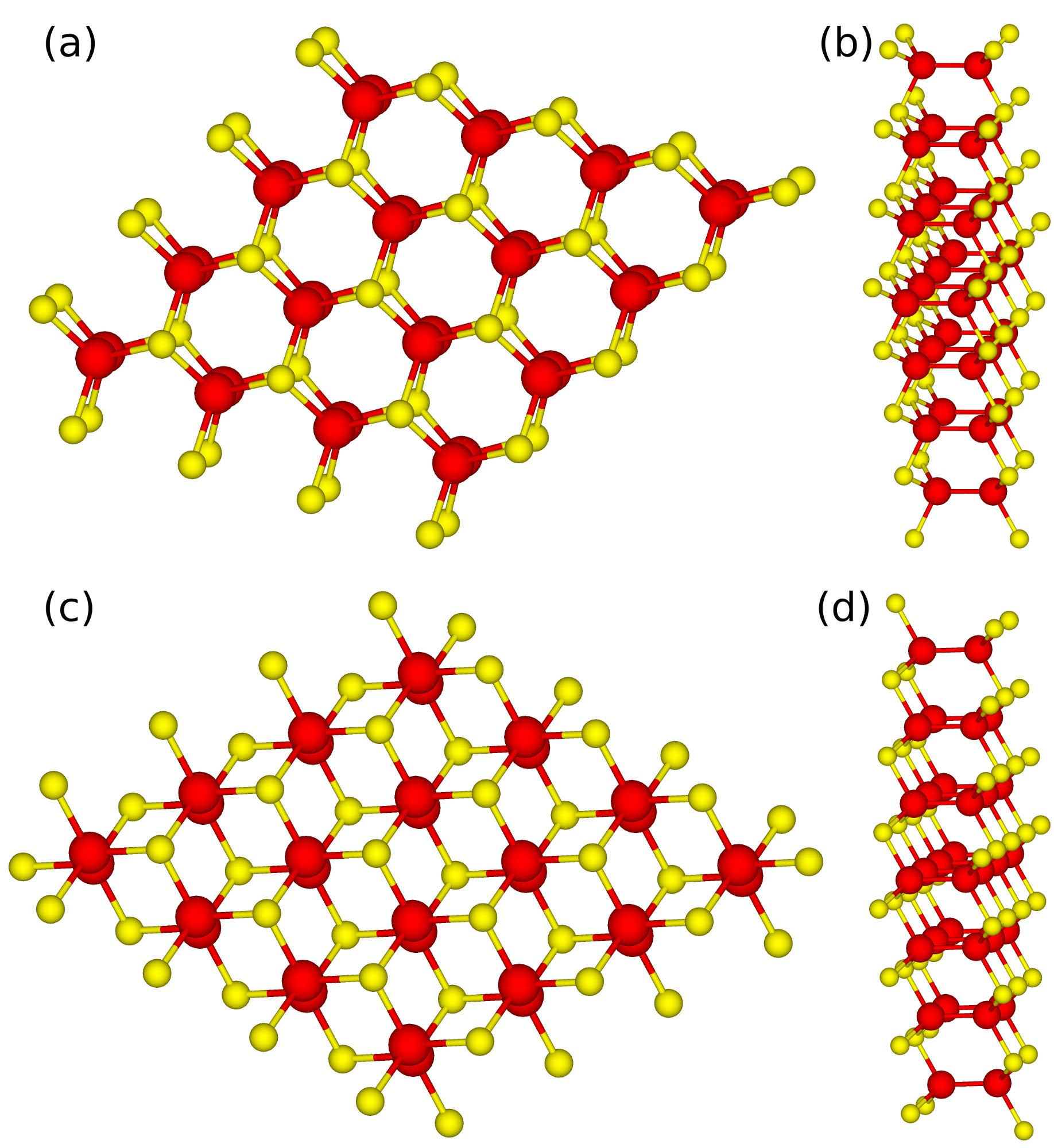
The post-transition-metal (PTM) atoms that we consider are indium and gallium, while the chalcogen atoms that we consider are sulfur, selenium, and tellurium. The PTM atoms are strongly bonded in vertical dimers lying on a hexagonal sublattice. Each PTM atom is strongly bonded to three chalcogen atoms lying on a different hexagonal sublattice to the PTM dimers. There are two different single-layer polytypes, as shown in Fig. 1: the chalcogen atoms may all lie on the same sublattice, or the top and bottom chalcogen atoms may lie on different sublattices [6, 7]. The former structure, referred to as the monolayer polytype, is slightly more stable and has vertical mirror symmetry about the center of the layer, although it lacks inversion symmetry (D3h point group). The latter structure, referred to as the monolayer polytype, does not have vertical mirror symmetry, but it does have inversion symmetry (D3d point group). In bulk hexagonal PTMCs there are further possibilities for polytypism due to the different ways in which the layers can be stacked. Our reference structure is the simplest possible bulk structure, which consists of AA-stacked -PTMC monolayers, with a four-atom primitive unit cell.
A range of polytypes and stacking orders have been reported for the bulk structures of the PTMCs obtained in experiments [51]. The [52] and [53] 2H polytypes both have reflection symmetry, with the former also having an inversion center. Meanwhile, the 3R polytype [54] has a single-layer primitive unit cell, and has neither inversion nor reflection symmetry. A polytype known as , consisting of a four-layer unit cell with two interfaces between successive layers stacked as in the polytype and the other two interfaces stacked as in the polytype, has also been reported for GaSe [55]. Note that the monolayer polytype should not be confused with the polytype of bulk PTMCs: the former refers to the inversion-symmetric monolayer shown in Figs. 1(c) and 1(d), the latter to the bulk crystal in which non-inversion-symmetric monolayers [the monolayer polytype shown in Figs. 1(a) and 1(b)] stack into an AB-type bulk crystal that now exhibits inversion symmetry. To avoid confusion, in Sec. II we adopt a notation for PTMC stacking that enables unambiguous characterization of all PTMC crystals irrespective of the monolayer polytypes or stacking order of successive layers.
The rest of this paper is structured as follows. Our approach for enumerating physically relevant PTMC structures is described in Sec. II. We present a fitting function to describe the energetics of PTMC polytypes in Sec. III. We compare the DFT energies of PTMC polytypes obtained with different exchange–correlation functionals in Sec. IV. Our analysis of the most stable polytypes, including the effects of pressure, is presented in Sec. V. We examine the relationship between the electronic band gap and the energetic stability of polytypes in Sec. VI. Finally, we draw our conclusions in Sec. VII. Our DFT simulation parameters can be found in Appendix A.
II Characterization of structures
The bulk hexagonal PTMC geometries we have examined are as follows. (i) We assume that each sublayer of chalcogen atoms and each sublayer of vertical PTM dimers lie at the A, B, or C hexagonal sublattice sites, because energy minima are overwhelmingly likely to occur at these high-symmetry configurations. (ii) We assume that each chalcogen sublayer lies on a different hexagonal sublattice to the PTM sublayer; our DFT calculations for InSe confirm that the energy is around 2 eV per monolayer unit cell higher each time the chalcogen atoms are on the same sublattice as the PTM dimers. In general a two-layer structure is a 2H polytype in Ramsdell notation [56], and a three-layer structure is a 3H polytype. However, there are exceptions; e.g., the structure is a 3R polytype with a rhombohedral primitive Bravais lattice. Nevertheless, for consistency and ease of automation, we have used a hexagonal unit cell in all our calculations.
We have performed DFT calculations for all such two-layer and three-layer bulk structures. We refer to each of these configurations by a character string summarizing the 2D hexagonal sublattice sites for each sublayer of atoms in the unit cell. Upper-case letters (A, B, and C) are used for PTM-dimer sublayers; lower-case letters (a, b, and c) are used for chalcogen sublayers. The 2D hexagonal sublattice sites for a single sublayer are shown in Fig. 2. For example, the string “aBabCa” describes a two-layer bulk structure in which the PTM dimers lie on the B and C sublattices, while the chalcogen atoms in the first layer are all at the A sublattice sites and the chalcogen atoms in the second layer are at the B and A sublattice sites. In this notation, the polytype [53] is aBabCb, the polytype [52] is aBabAb, the polytype [54] is aBabCbcAc, and the polytype [55] is aBabAbaCacAc.
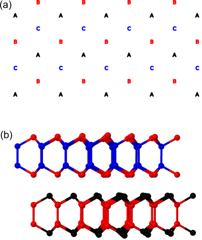
PTMC structures are energetically invariant if we perform any rigid operations (translations, rotations, or reflections). In-plane translations from one sublattice to another correspond to even permutations of the sublattice labels A, B, and C; thus, e.g., “aBabCa” is energetically equivalent to “bCbcAb.” In-plane point rotations through or reflections in vertical planes, together with translations, correspond to odd permutations of the sublattice labels; thus “aBabCa” is equivalent to “aCacBa.” PTMC structures are also equivalent under vertical displacements, which correspond to rotating the structure strings through three characters; thus “aBabCa” is equivalent to “bCaaBa.” Finally, structures are energetically invariant under reflections in horizontal planes; thus “aCacBa” is equivalent to “aBcaCa.”
A program was written to loop over all valid structure strings (i.e., strings in which each chalcogen atom is at a different sublattice site to the neighboring PTM dimer) for multilayer bulk structures. Energetically equivalent structure strings were eliminated and DFT input files for the remaining structures were generated. We find that there are inequivalent one-layer structures (these being the and polytypes with AA stacking), inequivalent two-layer structures (two of these being supercells of the one-layer structures), inequivalent three-layer structures, inequivalent four-layer structures, inequivalent five-layer structures, and inequivalent six-layer structures. The atomic positions and lattice vectors were relaxed within DFT at zero external pressure, subject to the constraint of the initial symmetry. The imposition of symmetry constrains the unit cell to be hexagonal and constrains the atoms to 2D hexagonal sites, but it allows the sublayers to relax in the out-of-plane direction and it also allows the and hexagonal lattice parameters to relax.
III Fit to the bulk PTMC energies
To represent the energy of each structure we fit
| (1) | |||||
to the energy per monolayer unit cell, where is the number of PTMC monolayers in structure , is the number of places in the unit cell in which neighboring chalcogen atoms are on different hexagonal sublattice sites, is the number of places in the unit cell in which PTM dimers in neighboring layers are on different hexagonal sites, is the number of -polytype layers in the unit cell, and is the number of places in which the next-nearest chalcogen atom is on the same hexagonal site as a PTM dimer. For our aBa reference structure (AA-stacked -PTMC), . Hence the fitting parameter describes the total energy per monolayer unit cell of the aBa structure. is the energy associated with neighboring chalcogen atoms lying on different hexagonal sublattice sites rather than the same sublattice site. is the energy associated with PTM dimers in neighboring layers not lying on the same sublattice. is the energy of the polytype of a single layer relative to the energy of the polytype. Finally, is the energy associated with second-nearest-neighbor chalcogen atoms lying on the same hexagonal site rather than different sublattice sites. The energy of structure relative to the aBa structure is .
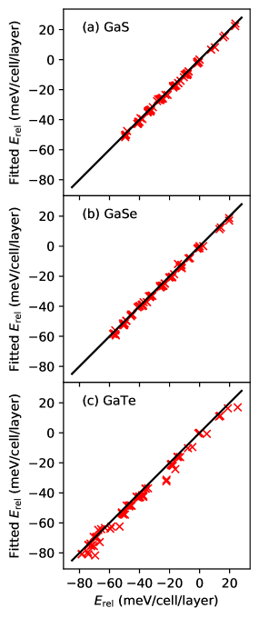
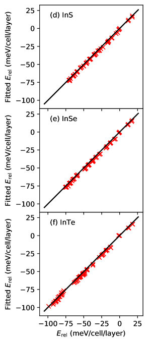
The quality of the resulting fits is illustrated for the DFT-PBE-MBD* data in Fig. 3. The fitted parameters and the root-mean-square (RMS) error in the fit per degree of freedom are reported in Table 1. The two- and three-layer structures are all distinct, with the sole exception of the aBa and aBc structures. These were independently relaxed for the two- and three-layer cases, and both the two- and three-layer versions were included in the fit. The DFT-PBE-MBD* energy difference between the equivalent two- and three-layer aBa and aBc structures is around – meV per monolayer unit cell, suggesting that the data suffer from a random error of this order of magnitude due to the finite -point sampling grids and uncertainties in the relaxed geometries. Thus the RMS errors shown in Table 1 are primarily due to noise in the data rather than any shortcoming in the fitting function of Eq. (1). The fit to the GaTe and InTe energy data is clearly significantly poorer than for the other PTMCs.
| PTMC | RMS error | |||||||||
|---|---|---|---|---|---|---|---|---|---|---|
| GaS | . | . | . | . | . | |||||
| GaSe | . | . | . | . | . | |||||
| GaTe | . | . | . | . | . | |||||
| InS | . | . | . | . | . | |||||
| InSe | . | . | . | . | . | |||||
| InTe | . | . | . | . | . | |||||
IV Comparison of DFT functionals
We have computed the DFT energies within the local density approximation (LDA) and the Perdew-Burke-Ernzerhof (PBE) variant of the generalized gradient approximation [57]. We compare a representative set of semiempirical dispersion-correction schemes: Grimme 2006 (G06) [58]; Ortmann, Bechstedt, and Schmidt (OBS) [59]; and the many-body dispersion (MBD*) method [60, 61]. We have also investigated the optB86b (MK) and optB88 (BO) nonlocal van der Waals density functionals [62]. DFT simulation parameters such as the plane-wave cutoff energy are summarized in Appendix A.
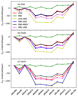
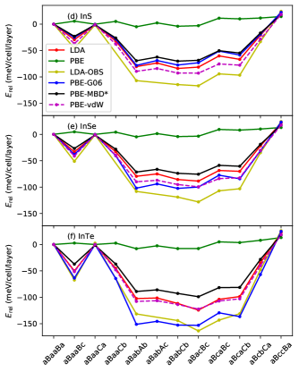
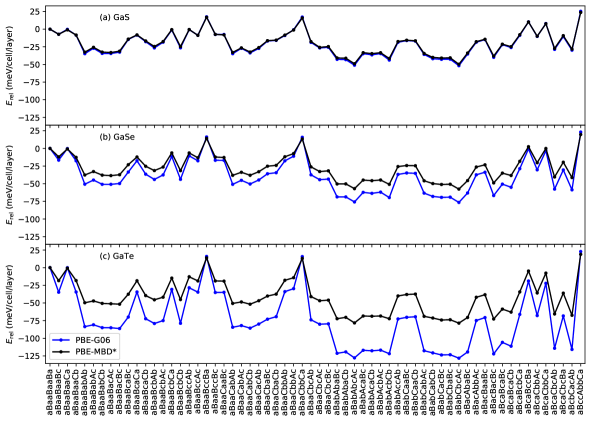
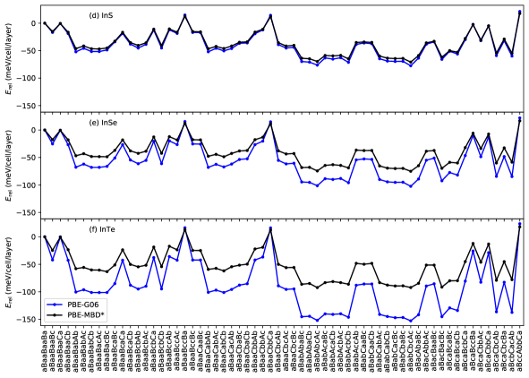
We obtained a complete set of DFT-PBE-G06 and DFT-PBE-MBD* total-energy results for all two- and three-layer structures and fitted Eq. (1) to the data. We also obtained DFT-LDA, DFT-PBE, DFT-LDA-OBS, and vdW-DF data for all two-layer structures, to assess the performance of these functionals. The DFT results for two-layer structures are shown in Fig. 4. The corresponding results for three-layer structures are shown in Fig. 5. The disagreements between different dispersion corrections indicate the limitations of DFT in studies of layered structures. Alternative methods such as quantum Monte Carlo approaches are required to provide independent benchmarks [63]. We regard the DFT-PBE-MBD* method as somewhat more reliable than the other dispersion corrections because it describes many-body interactions and screening effects beyond a description by pairwise interatomic potentials, and because it has been extensively benchmarked against diffusion quantum Monte Carlo data [64].
V Structural stability
V.1 Zero external pressure
Using Eq. (1) together with the parameters shown in Table 1, we find that for GaS, GaSe, GaTe, and InS the most stable hexagonal structure is aBabAb, which corresponds to the polytype described in experiments [52]. This structure consists of an AA′ stacking of -polytype monolayers and has D6h point group and P/mmc space group. For GaSe, this structure is more stable than the and polytypes by meV per monolayer unit cell, and it is more stable than the polytype by a mere meV per monolayer unit cell. The most energetically stable structures of GaSe with unit cells of up to six layers are shown in Table 2.
| Structure | Energy (meV/cell/layer) |
|---|---|
| aBabAb (-GaSe) | |
| aBabAbaBabAbaBabCb | |
| aBabAbaBabAbaBacAc | |
| aBabAbaBabAbaCacAc | |
| aBabAbaBabCbcBcbCb | |
| aBabAbaCacAc (-GaSe) | |
| aBabAbaBabCb | |
| aBabAbaBacAc | |
| aBabAbaBabCbcAc | |
| aBabAbaCacAcbCb | |
| aBabAbaBabCbaBabCb | |
| aBabAbaBabCbaBacAc | |
| aBabAbaBabCbcAcbCb | |
| aBabAbaBacAcaBacAc | |
| aBabAbaBacAcbCbcAc | |
| aBabAbaCabAbaBabCb | |
| aBabAbaCabAbaBacAc | |
| aBabAbaCabAbaCacAc | |
| aBabAbaCabAbcBcbCb | |
| aBabAbaCacAcbCbcAc | |
| aBabAbaCacBcbCbcAc | |
| aBabAbcBcbAbaBacAc | |
| aBabCb (-GaSe) | |
| aBabCbcAc (-GaSe) | |
| aBacBc |
On the other hand, for InSe and InTe the most stable hexagonal structure is aBacBc. This consists of an AB′ stacking of -polytype monolayers. For InSe this structure is more stable than the and polytypes (aBabCb and aBabCbcAc) by just meV per monolayer unit cell. The most stable structure differs from that of the gallium chalcogenides and indium sulfide by a horizontal translation of every second layer. Nevertheless, this structure also has D6h point group and P/mmc space group. The most stable structures of InSe in unit cells of up to six layers are shown in Table 3.
| Structure | Energy (meV/cell/layer) |
|---|---|
| aBacBc | |
| aBabCbaBacBcaBacBc | |
| aBabCbaCabCbaBacBc | |
| aBabCbaCabCbaCabCb | |
| aBabCbaCabCbaCacBc | |
| aBabCbaBacBc | |
| aBabCbaCabCb | |
| aBabCbaCacBc | |
| aBabCbaCabAbcAc | |
| aBabCbaCabCbcAc | |
| aBabCbaBabCbaBacBc | |
| aBabCbaBabCbaCabCb | |
| aBabCbaBabCbaCacBc | |
| aBabCbaBacAcaBacBc | |
| aBabCbaBacAcbAbcAc | |
| aBabCbaBacAcbAbcBc | |
| aBabCbaBacBcaCacBc | |
| aBabCbaBacBcbAbcBc | |
| aBabCbaCabAbaCabCb | |
| aBabCbaCabAbaCacBc | |
| aBabCbaCabCbaBacAc | |
| aBabCbaCacBcbAbcAc | |
| aBabCb (-InSe) | |
| aBabCbcAc (-InSe) | |
| aBabAbaCacAc (-InSe) | |
| aBabAb (-InSe) |
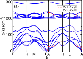
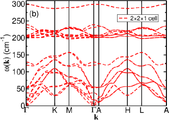
As a test, we have relaxed the structures of aBabAb (the polytype) and aBabCb (the polytype) GaSe without any symmetry constraints. The initial lattice vectors and atom positions were randomly offset by a small amount from their exact hexagonal-cell values, and the positions and lattice vectors were relaxed within DFT-PBE-MBD* at zero pressure. This did not lead to a lowering of the total energy relative to the hexagonal cell, thus providing direct evidence in support of our assumption that the unit cell is hexagonal in all cases and that the atoms lie in horizontal sublayers on hexagonal sublattice sites. Direct confirmation that the structures that we have found to be most energetically stable in any of the PTMCs are also dynamically stable is provided by the DFT-PBE-MBD* phonon dispersion curves shown in Fig. 6. On the other hand, it is known that a monoclinic structure of GaTe is more stable than the hexagonal structures studied here [66, 67].
While experimental results [55, 53, 52, 54, 68] support our determination of the monolayer structure as the most stable form, and also agree that the most stable structure of GaS is aBabAb (the polytype) [52], for InSe and GaSe the aBacBc structure calculated to be most stable is not one of the commonly observed structures in experiments. Specifically, the experimental work on InSe finds most often the polytype (aBabCbcAc) [54] and occasionally the polytype (aBabCb) [68], neither of which has inversion symmetry. For GaSe the polytype (aBabCb) [53] and the polytype (aBabCbcBcbAb) [55] are reported, against our result of aBabAb (the polytype). It should be noted that our results show several structures for each PTMC of comparable stability on a sub-meV-per-monolayer-unit-cell scale. This has important consequences, not only on the theoretical side, with the structure returned as the most stable being sensitive to the van der Waals functional chosen, but also on the experimental side, suggesting that the polytype of a PTMC crystal must be highly sensitive to the crystal growth conditions. Indeed, it supports the observation of multiple stacking faults and regions of different polytypes within a single sample [69], and suggests that the synthesis of different PTMC polytypes should be possible with careful tuning of experimental conditions. On the theoretical side, an important conclusion is that a computational method with an accuracy and precision of around meV per monolayer unit cell is required to determine the most stable PTMC structure reliably. The meV per monolayer unit cell spread of DFT results with different van der Waals correction schemes and the meV per monolayer unit cell disagreement between independently relaxed equivalent two- and three-layer structures, together with the disagreements with experiment regarding the most stable structures, demonstrate that dispersion-corrected DFT is not currently capable of such accuracy and precision.
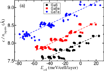
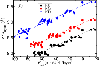
We compare our relaxed lattice parameters with both previous DFT results and experimental results in Table 4. Where comparison is possible, our dispersion-corrected DFT-PBE calculations agree with experimental results to within Å (often an order of magnitude better). The hexagonal lattice parameter is almost the same for all structures of a given PTMC, reflecting the in-plane rigidity of the individual layers. However, the lattice parameter is much more sensitive to the structure, as shown in Fig. 7. High-energy structures generally have larger lattice parameters .
| -GaS (aBabAb) | -GaSe (aBabCb) | -InSe (aBabCbcAc) | ||||
| Method | (Å) | (Å) | (Å) | (Å) | (Å) | (Å) |
| DFT-LDA | 3.541 | 15.214 | 3.762 | 15.666 | ||
| DFT-LDA-OBS | 3.517 | 14.939 | 3.695 | 15.346 | ||
| DFT-PBE | 3.633 [67], 3.626 | 16.677 [67], 17.633 | 3.823 [67], 3.811 | 17.848 [67], 18.201 | 4.091 [67] | 26.982 [67] |
| DFT-PBE-G06 | 3.570 | 15.497 | 3.740 | 15.899 | 3.942 | 25.251 |
| DFT-PBE-MBD* | 3.583 | 15.266 | 3.771 | 15.744 | 4.031 | 24.919 |
| vdW-DF2-C09 | 3.575 [67] | 15.460 [67] | 3.761 [67] | 15.943 [67] | 4.028 [67] | 24.996 [67] |
| Experiment | 3.587 [52] | 15.492 [52] | 3.743 [70] | 15.919 [70] | 4.002 [54] | 24.946 [54] |
V.2 Nonzero pressure
At zero temperature the most thermodynamically stable polytype is the structure with the lowest enthalpy . At sufficiently low pressures we may approximate the enthalpy of a PTMC structure as
| (2) |
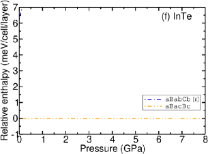
where and are the zero-pressure energy and volume. The enthalpy is plotted against pressure for energetically competitive structures of gallium chalcogenides and indium chalcogenides in Fig. 8. Of the two-layer structures, aBabCb (the polytype), aBacBc, and (in GaS, GaSe, and InS) aBabAb (the polytype), have DFT-PBE-MBD* energies within a few meV per monolayer cell of each other at zero pressure, but at higher pressure, aBabAb (the polytype) is clearly disfavored. More generally, the application of pressure simplifies the picture by reducing the number of competing structures and increasing the relative enthalpies of those structures. In GaSe, the three-layer structures aBabCbcAc (the polytype) and aBabAbcAc are competitive at low pressure. This is not the case in InSe. However, at very high pressures, three-layer structures may be favored in InSe. Below 7.1 GPa, the aBacBc structure of InSe is favored; above 7.1 GPa, the aBacBacBc structure of InSe is favored. The structures favored at high pressures feature PTM dimers on the same sublattice and neighboring chalcogen atoms on different sublattices, as would be expected from steric considerations. At low pressure it is once again clear that accuracy and precision of around meV per monolayer unit cell are required to identify the most stable polytype unambiguously.
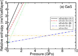
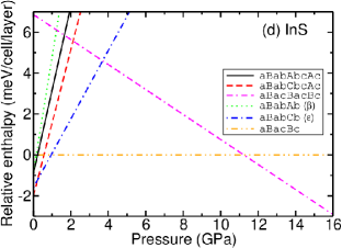
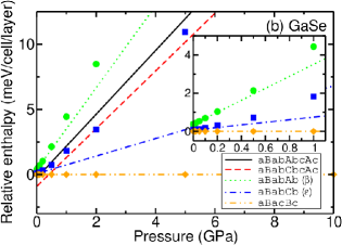
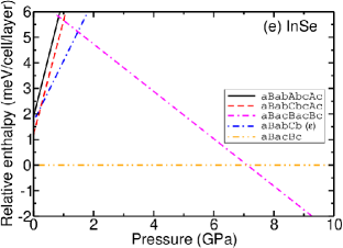

In Fig. 8(b) we compare the linear approximation to the enthalpy [Eq. 2)] with DFT enthalpies obtained by directly relaxing the lattice vectors at a given external pressure. We find that the linear approximation is of quantitative accuracy on a meV-per-monolayer-unit-cell scale for relative enthalpies up to around GPa. Beyond this, the linear approximation provides a qualitative picture that generally preserves the ordering of the structures, at least up to GPa.
In all bulk PTMCs at multi-GPa pressures, the aBacBc structure is found to be the most stable structure over a broad range of pressures in DFT-PBE-MBD* calculations. This is the inversion-symmetric structure that is predicted to be most stable for InSe and InTe at zero pressure, and consists of AB′-stacked monolayers. Despite its ubiquitous presence in the theoretical calculations, we are not aware that this structure has previously been reported.
VI Electronic band structure
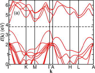
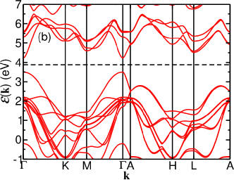
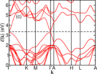
In Fig. 9 we plot the DFT-PBE electronic band structures of the theoretically most stable polytypes of GaSe and InSe (aBabAb and aBacBc, respectively) and the experimentally observed [53] polytype (aBabCb) of GaSe. The structures were relaxed using DFT-PBE-MBD*. In each case the polytypes exhibit a direct band gap at the point of the two-layer hexagonal Brillouin zone. The DFT-PBE band gaps, which are expected to be significant underestimates of the true gaps [71], are and eV for the aBabAb and aBabCb structures of GaSe, respectively. The low-energy band structure is qualitatively similar for these two energetically competitive structures of GaSe. The DFT-PBE band gap of the most stable structure of InSe (aBacBc) is much smaller than the gap of GaSe, at eV.

We have examined the band gap of a range of two-layer structures for each material, finding that the vertical band gap at and the ground-state energy of each structure are positively correlated, although with significant noise: see Fig. 10. PTMC structures with smaller band gaps tend to be more stable. In fact, the most stable two-layer structure of InTe has a direct gap at of just meV. In most cases the vertical gap at is the fundamental gap, especially for low-energy structures. A notable exception is GaTe, where the vertical gap at is nonfundamental for all the two-layer structures. In the most stable two-layer GaTe structure, the valence-band maximum is at but the conduction-band minimum is on the – line. Previous work using DFT and many-body perturbation theory has shown that -InSe changes from a direct-gap material to an indirect-gap material under high pressure [72].
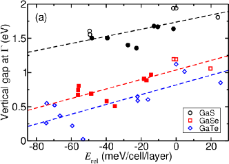
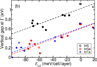
The experimentally measured gaps of -InSe, -InSe and -InSe are eV [73], – eV [74, 75], and eV [76], respectively, which are (as expected) very much larger than the DFT-PBE InSe gaps of energetically stable polytypes shown in Fig. 10. Nevertheless, we would expect the qualitative conclusion that the band gap of a PTMC polytype is positively correlated with its energy to continue to hold.
We note that the dispersion of the band-edge states in the out-of-plane direction along -A is substantial. The electronic structure is very much three-dimensional, despite the layered crystalline structure of the PTMCs. This dispersion arises due to strong interlayer hybridization of orbital states on chalcogen atoms in the band-edge wave functions [38]. It is the restriction of out-of-plane momentum in ultrathin PTMC films that gives rise to their strong thickness-dependent electronic and optical properties, with an increase in band gap for a reduced number of layers [13, 14].
VII Conclusions
We have used dispersion-corrected DFT methods to examine the relative stability of a large number of candidate bulk hexagonal PTMC polytypes. For all PTMCs there is a clear consensus among DFT functionals that the monolayer polytype, in which the chalcogen atoms lie on the same hexagonal sublattice, is – meV per monolayer unit cell more stable than the polytype, in which the chalcogen atoms lie on different hexagonal sublattices; indeed, all experimentally observed bulk polytypes only feature monolayers [55, 53, 52, 54, 68]. Our DFT-PBE-MBD* calculations show that there is an energy gain of – meV per monolayer unit cell from having neighboring chalcogen atoms on different hexagonal sublattices; again, all experimentally observed polytypes only have neighboring chalcogen atoms on different hexagonal sublattices [55, 53, 52, 54, 68]. The DFT-PBE-MBD* energy gain associated with PTM dimers in neighboring layers lying on different hexagonal sublattices is – meV per monolayer unit cell. This leads to a tendency to avoid AA-stacked structures at zero pressure. However, in InSe and InTe this is offset by an energy penalty of – meV per monolayer unit cell associated with PTM dimers and next-nearest chalcogen atoms lying the same hexagonal sublattices; it is geometrically impossible to have an AB- or ABC-stacked structure in which PTM dimers and next-nearest chalcogen atoms all lie on different hexagonal sublattices. The interplay between these effects leads to a subtle, sub-meV competition between polytypes. Disagreements between dispersion-corrected DFT total energies are of order meV per monolayer unit cell. Disagreements between the relative energies of the lowest-energy polytypes are of order – meV per monolayer unit cell. Only for GaS is the observed stable polytype () predicted by DFT-PBE-MBD* to have the lowest energy; however, in GaSe and InSe the observed polytypes are very close in energy to the theoretically most stable structure. We conclude that dispersion-corrected DFT methods are not yet able to predict the relative stability of bulk PTMC polymorphs reliably; however, they can provide insights into the energy scales involved and the types of structures that are favored. The small energy differences between competing polytypes imply that a wide variety of different polytypes are likely to be found in experiments, and that stacking faults must be common in PTMC samples.
We find that application of pressure tends to favor an aBacBc PTMC structure that has not previously been reported. In fact this polytype is found to be most stable within DFT-PBE-MBD* at zero pressure for InSe and InTe. We also find that there is a positive correlation between the ground-state total energy and the electronic band gap; energetically stable PTMC polytypes tend to have smaller band gaps.
Acknowledgements.
We acknowledge useful conversations with V. I. Fal’ko. All relevant data present in this publication can be accessed at URL???. Computational resources were provided by Lancaster University’s high-end computing facility, and by the University of Manchester Computational Shared Facility. SJM acknowledges support from EC Quantum Technology Flagship Project No. 2D-SIPC.Appendix A Methodology
We used DFT as implemented in the castep [77] plane-wave-basis code to compute the relative energies of PTMC crystals in a variety of bulk hexagonal structures. We used ultrasoft pseudopotentials to represent atomic cores and we used plane-wave cutoff energies of at least eV. The maximum distance between points in the Monkhorst-Pack grid was less than Å-1 in each case. The force tolerance for geometry optimization was meV Å-1. We verified that near-identical relative energies for PTMC structures were obtained using the vasp [78] DFT code with projector augmented-wave (PAW) pseudopotentials instead of castep. In the vasp calculations the basis consisted of plane waves with a cutoff energy of eV and the Brillouin zone was sampled by a Monkhorst-Pack grid of points. The crystals were fully optimized with a force tolerance of eV Å-1. We also verified that castep DFT relative energies obtained using norm-conserving pseudopotentials were in agreement (on a meV-per-monolayer-unit-cell scale) with our results obtained using ultrasoft pseudopotentials. Full data sets can be found in the Supplemental Information [65].
References
- Schubert and Dörre [1953] K. Schubert and E. Dörre, Kristallstrukturen des GaSe, Naturwiss. 40, 604 (1953).
- Hahn and Frank [1955] H. Hahn and G. Frank, Über die Kristallstruktur des GaS, Z. Anorg. Allg. Chem. 278, 340 (1955).
- Sugaike [1957] S. Sugaike, Synthesis, crystal lattices and some electrical properties of indium tellurides and selenides, Mineral. J. 2, 63 (1957).
- Late et al. [2012] D. J. Late, B. Liu, J. Luo, A. Yan, H. S. S. R. Matte, M. Grayson, C. N. R. Rao, and V. P. Dravid, GaS and GaSe ultrathin layer transistors, Adv. Mater. 24, 3549 (2012).
- Hu et al. [2012] P. Hu, Z. Wen, L. Wang, P. Tan, and K. Xiao, Synthesis of few-layer GaSe nanosheets for high performance photodetectors, ACS Nano 6, 5988 (2012).
- Zólyomi et al. [2013] V. Zólyomi, N. D. Drummond, and V. I. Fal’ko, Band structure and optical transitions in atomic layers of hexagonal gallium chalcogenides, Phys. Rev. B 87, 195403 (2013).
- Zólyomi et al. [2014] V. Zólyomi, N. D. Drummond, and V. I. Fal’ko, Electrons and phonons in single layers of hexagonal indium chalcogenides from ab initio calculations, Phys. Rev. B 89, 205416 (2014).
- Tamalampudi et al. [2014] S. R. Tamalampudi, Y.-Y. Lu, R. K. U., Raman Sankar, C.-D. Liao, K. M. B., C.-H. Cheng, F. C. Chou, and Y.-T. Chen, High performance and bendable few-layered InSe photodetectors with broad spectral response, Nano Lett. 14, 2800 (2014).
- Liu et al. [2014] F. Liu, H. Shimotani, H. Shang, T. Kanagasekaran, V. Zólyomi, N. Drummond, V. I. Fal’ko, and K. Tanigaki, High-sensitivity photodetectors based on multilayer GaTe flakes, ACS Nano 8, 752 (2014).
- Cao et al. [2015] T. Cao, Z. Li, and S. G. Louie, Tunable magnetism and half-metallicity in hole-doped monolayer GaSe, Phys. Rev. Lett. 114, 236602 (2015).
- Mudd et al. [2015] G. W. Mudd, S. A. Svatek, L. Hague, O. Makarovsky, Z. R. Kudrynskyi, C. J. Mellor, P. H. Beton, L. Eaves, K. S. Novoselov, Z. D. Kovalyuk, E. E. Vdovin, A. J. Marsden, N. R. Wilson, and A. Patanè, High broad-band photoresponsivity of mechanically formed InSe-graphene van der Waals heterostructures, Adv. Mater. 27, 3760 (2015).
- Sucharitakul et al. [2015] S. Sucharitakul, N. J. Goble, U. R. Kumar, Raman Sankar, Z. A. Bogorad, F.-C. Chou, Y.-T. Chen, and X. P. A. Gao, Intrinsic electron mobility exceeding 103 cm2/(V s) in multilayer InSe FETs, Nano Lett. 15, 3815 (2015).
- Bandurin et al. [2016] D. A. Bandurin, A. V. Tyurnina, G. L. Yu, A. Mishchenko, V. Zólyomi, S. V. Morozov, R. K. Kumar, R. V. Gorbachev, Z. R. Kudrynskyi, S. Pezzini, Z. D. Kovalyuk, U. Zeitler, K. S. Novoselov, A. Patanè, L. Eaves, I. V. Grigorieva, V. I. Fal’ko, A. K. Geim, and Y. Cao, High electron mobility, quantum Hall effect and anomalous optical response in atomically thin InSe, Nat. Nanotechnol. 12, 223 (2016).
- Ben Aziza et al. [2017] Z. Ben Aziza, D. Pierucci, H. Henck, M. G. Silly, C. David, M. Yoon, F. Sirotti, K. Xiao, M. Eddrief, J.-C. Girard, and A. Ouerghi, Tunable quasiparticle band gap in few-layer GaSe/graphene van der Waals heterostructures, Phys. Rev. B 96, 035407 (2017).
- Hung et al. [2017] N. T. Hung, A. R. T. Nugraha, and R. Saito, Two-dimensional InSe as a potential thermoelectric material, Appl. Phys. Lett. 111, 092107 (2017).
- Terry et al. [2018] D. J. Terry, V. Zólyomi, M. Hamer, A. V. Tyurnina, D. G. Hopkinson, A. M. Rakowski, S. J. Magorrian, N. Clark, Y. M. Andreev, O. Kazakova, K. Novoselov, S. J. Haigh, V. I. Fal’ko, and R. Gorbachev, Infrared-to-violet tunable optical activity in atomic films of GaSe, InSe, and their heterostructures, 2D Mater. 5, 041009 (2018).
- Hamer et al. [2019] M. J. Hamer, J. Zultak, A. V. Tyurnina, V. Zólyomi, D. Terry, A. Barinov, A. Garner, J. Donoghue, A. P. Rooney, V. Kandyba, A. Giampietri, A. Graham, N. Teutsch, X. Xia, M. Koperski, S. J. Haigh, V. I. Fal’ko, R. V. Gorbachev, and N. R. Wilson, Indirect to direct gap crossover in two-dimensional InSe revealed by angle-resolved photoemission spectroscopy, ACS Nano 13, 2136 (2019).
- Voitchovsky and Mercier [1974] J. P. Voitchovsky and A. Mercier, Photoluminescence of GaSe, Il Nuovo Cimento B 22, 273 (1974).
- Camassel et al. [1978] J. Camassel, P. Merle, H. Mathieu, and A. Chevy, Excitonic absorption edge of indium selenide, Phys. Rev. B 17, 4718 (1978).
- Alekperov et al. [1991] O. Alekperov, M. Godjaev, M. Zarbaliev, and R. Suleimanov, Interband photoconductivity in layer semiconductors GaSe, InSe and GaS, Solid State Commun. 77, 65 (1991).
- Ho and Lin [2006] C. H. Ho and S. L. Lin, Optical properties of the interband transitions of layered gallium sulfide, J. Appl. Phys. 100, 083508 (2006).
- Tredgold and Clark [1969] R. Tredgold and A. Clark, Hopping conduction in gallium selenide single crystals, Solid State Commun. 7, 1519 (1969).
- Ottaviani et al. [1974] G. Ottaviani, C. Canali, F. Nava, P. Schmid, E. Mooser, R. Minder, and I. Zschokke, GaSe: A layer compound with anomalous valence band anisotropy, Solid State Commun. 14, 933 (1974).
- Schlüter et al. [1976] M. Schlüter, J. Camassel, S. Kohn, J. P. Voitchovsky, Y. R. Shen, and M. L. Cohen, Optical properties of GaSe and GaSxSe1-x mixed crystals, Phys. Rev. B 13, 3534 (1976).
- Kuroda et al. [1980] N. Kuroda, I. Munakata, and Y. Nishina, Exciton transitions from spin-orbit split off valence bands in layer compound InSe, Solid State Commun. 33, 687 (1980).
- Kress-Rogers et al. [1982] E. Kress-Rogers, R. Nicholas, J. Portal, and A. Chevy, Cyclotron resonance studies on bulk and two-dimensional conduction electrons in InSe, Solid State Commun. 44, 379 (1982).
- Gomes da Costa et al. [1993] P. Gomes da Costa, R. G. Dandrea, R. F. Wallis, and M. Balkanski, First-principles study of the electronic structure of -InSe and -InSe, Phys. Rev. B 48, 14135 (1993).
- Fernelius [1994] N. Fernelius, Properties of gallium selenide single crystal, Prog. Cryst. Growth Ch. 28, 275 (1994).
- Cingolani et al. [1981] A. Cingolani, M. Ferrara, M. Lugarà, and F. Lévy, Optical gain in gallium selenide and indium selenide, Physica B 105, 40 (1981).
- Segura et al. [1997] A. Segura, J. Bouvier, M. V. Andrés, F. J. Manjón, and V. Muñoz, Strong optical nonlinearities in gallium and indium selenides related to inter-valence-band transitions induced by light pulses, Phys. Rev. B 56, 4075 (1997).
- Singh et al. [1998] N. Singh, D. Suhre, V. Balakrishna, M. Marable, R. Meyer, N. Fernelius, F. Hopkins, and D. Zelmon, Far-infrared conversion materials: Gallium selenide for far-infrared conversion applications, Prog. Cryst. Growth Ch. 37, 47 (1998).
- Allakhverdiev et al. [2009] K. R. Allakhverdiev, M. O. Yetis, S. Özbek, T. K. Baykara, and E. Y. Salaev, Effective nonlinear GaSe crystal. optical properties and applications, Laser Phys. 19, 1092 (2009).
- Segura et al. [1984] A. Segura, F. Pomer, A. Cantarero, W. Krause, and A. Chevy, Electron scattering mechanisms in -type indium selenide, Phys. Rev. B 29, 5708 (1984).
- Segura et al. [1979] A. Segura, A. Chevy, J. Guesdon, and J. Besson, Photovoltaic efficiency of InSe solar cells, Sol. Energy Mater. 2, 159 (1979).
- Segura et al. [1983] A. Segura, J. P. Guesdon, J. M. Besson, and A. Chevy, Photoconductivity and photovoltaic effect in indium selenide, J. Appl. Phys. 54, 876 (1983).
- Gibson et al. [2005] G. A. Gibson, A. Chaiken, K. Nauka, C. C. Yang, R. Davidson, A. Holden, R. Bicknell, B. S. Yeh, J. Chen, H. Liao, S. Subramanian, D. Schut, J. Jasinski, and Z. Liliental-Weber, Phase-change recording medium that enables ultrahigh-density electron-beam data storage, Appl. Phys. Lett. 86, 051902 (2005).
- Ben Aziza et al. [2018] Z. Ben Aziza, V. Zólyomi, H. Henck, D. Pierucci, M. G. Silly, J. Avila, S. J. Magorrian, J. Chaste, C. Chen, M. Yoon, K. Xiao, F. Sirotti, M. C. Asensio, E. Lhuillier, M. Eddrief, V. I. Fal’ko, and A. Ouerghi, Valence band inversion and spin-orbit effects in the electronic structure of monolayer GaSe, Phys. Rev. B 98, 115405 (2018).
- Magorrian et al. [2016] S. J. Magorrian, V. Zólyomi, and V. I. Fal’ko, Electronic and optical properties of two-dimensional InSe from a DFT-parametrized tight-binding model, Phys. Rev. B 94, 245431 (2016).
- Ritschel et al. [2018] T. Ritschel, H. Berger, and J. Geck, Stacking-driven gap formation in layered 1T-TaS2, Phys. Rev. B 98, 195134 (2018).
- Lee et al. [2019] S.-H. Lee, J. S. Goh, and D. Cho, Origin of the insulating phase and first-order metal-insulator transition in 1T-TaS2, Phys. Rev. Lett. 122, 106404 (2019).
- Stahl et al. [2020] Q. Stahl, M. Kusch, F. Heinsch, G. Garbarino, N. Kretzschmar, K. Hanff, K. Rossnagel, J. Geck, and T. Ritschel, Collapse of layer dimerization in the photo-induced hidden state of 1T-TaS2, Nat. Commun. 11, 10.1038/s41467-020-15079-1 (2020).
- Enaldiev et al. [2020] V. V. Enaldiev, V. Zólyomi, C. Yelgel, S. J. Magorrian, and V. I. Fal’ko, Stacking domains and dislocation networks in marginally twisted bilayers of transition metal dichalcogenides, Phys. Rev. Lett. 124, 206101 (2020).
- Weston et al. [2020] A. Weston, Y. Zou, V. Enaldiev, A. Summerfield, N. Clark, V. Zólyomi, A. Graham, C. Yelgel, S. Magorrian, M. Zhou, J. Zultak, D. Hopkinson, A. Barinov, T. H. Bointon, A. Kretinin, N. R. Wilson, P. H. Beton, V. I. Fal’ko, S. J. Haigh, and R. Gorbachev, Atomic reconstruction in twisted bilayers of transition metal dichalcogenides, Nat. Nanotechnol. 10.1038/s41565-020-0682-9 (2020).
- Chitara and Ya’akobovitz [2018] B. Chitara and A. Ya’akobovitz, Elastic properties and breaking strengths of GaS, GaSe and GaTe nanosheets, Nanoscale 10, 13022 (2018).
- Zhao et al. [2019] Q. Zhao, R. Frisenda, T. Wang, and A. Castellanos-Gomez, InSe: a two-dimensional semiconductor with superior flexibility, Nanoscale 11, 9845 (2019).
- Demirci et al. [2017] S. Demirci, N. Avazlı, E. Durgun, and S. Cahangirov, Structural and electronic properties of monolayer group III monochalcogenides, Phys. Rev. B 95, 115409 (2017).
- d’Amour et al. [1982] H. d’Amour, W. Holzapfel, A. Polian, and A. Chevy, Crystal structure of a new high pressure polymorph of GaS, Solid State Commun. 44, 853 (1982).
- Ulrich et al. [1996] C. Ulrich, M. A. Mroginski, A. R. Goñi, A. Cantarero, U. Schwarz, V. Muñoz, and K. Syassen, Vibrational properties of InSe under pressure: Experiment and theory, Phys. Status Solidi (b) 198, 121 (1996).
- Errandonea et al. [1999] D. Errandonea, A. Segura, V. Muñoz, and A. Chevy, Effects of pressure and temperature on the dielectric constant of GaS, GaSe, and InSe: Role of the electronic contribution, Phys. Rev. B 60, 15866 (1999).
- Errandonea et al. [2005] D. Errandonea, A. Segura, F. J. Manjón, A. Chevy, E. Machado, G. Tobias, P. Ordejón, and E. Canadell, Crystal symmetry and pressure effects on the valence band structure of -InSe and -GaSe: Transport measurements and electronic structure calculations, Phys. Rev. B 71, 125206 (2005).
- Gouskov et al. [1982] A. Gouskov, J. Camassel, and L. Gouskov, Growth and characterization of III-VI layered crystals like GaSe, GaTe, InSe, GaSe1-xTex and GaxIn1-xSe, Prog. Cryst. Growth Charact. 5, 323 (1982).
- Kuhn et al. [1976] A. Kuhn, A. Chevy, and R. Chevalier, Refinement of the 2H GaS -type, Acta Crystallogr. B 32, 983 (1976).
- Kuhn et al. [1975a] A. Kuhn, A. Chevy, and R. Chevalier, Crystal structure and interatomic distances in GaSe, Phys. Status Solidi (a) 31, 469 (1975a).
- Rigoult et al. [1980] J. Rigoult, A. Rimsky, and A. Kuhn, Refinement of the 3R -indium monoselenide structure type, Acta Crystallogr. B 36, 916 (1980).
- Kuhn et al. [1975b] A. Kuhn, R. Chevalier, and A. Rimsky, Atomic structure of a 4H GaSe polytype named -type, Acta Crystallogr. B 31, 2841 (1975b).
- Ramsdell [1947] L. S. Ramsdell, Studies on silicon carbide, Am. Mineral. 32, 64 (1947).
- Perdew et al. [1996] J. P. Perdew, K. Burke, and M. Ernzerhof, Generalized gradient approximation made simple, Phys. Rev. Lett. 77, 3865 (1996).
- Grimme [2006] S. Grimme, Semiempirical GGA-type density functional constructed with a long-range dispersion correction, J. Comp. Chem. 27, 1787 (2006).
- Ortmann et al. [2006] F. Ortmann, F. Bechstedt, and W. G. Schmidt, Semiempirical van der Waals correction to the density functional description of solids and molecular structures, Phys. Rev. B 73, 205101 (2006).
- Tkatchenko et al. [2012] A. Tkatchenko, R. A. DiStasio, R. Car, and M. Scheffler, Accurate and efficient method for many-body van der Waals interactions, Phys. Rev. Lett. 108, 236402 (2012).
- Ambrosetti et al. [2014a] A. Ambrosetti, A. M. Reilly, R. A. DiStasio, and A. Tkatchenko, Long-range correlation energy calculated from coupled atomic response functions, J. Chem. Phys. 140, 18A508 (2014a).
- Klimeš et al. [2009] J. Klimeš, D. R. Bowler, and A. Michaelides, Chemical accuracy for the van der Waals density functional, J. Phys. Condens. Mater. 22, 022201 (2009).
- Mostaani et al. [2015] E. Mostaani, N. D. Drummond, and V. I. Fal’ko, Quantum Monte Carlo calculation of the binding energy of bilayer graphene, Phys. Rev. Lett. 115, 115501 (2015).
- Ambrosetti et al. [2014b] A. Ambrosetti, D. Alfè, R. A. DiStasio, and A. Tkatchenko, Hard numbers for large molecules: Toward exact energetics for supramolecular systems, J. Phys. Chem. Lett. 5, 849 (2014b).
- [65] See Supplemental Information at [URL???] for tables comparing the DFT relative energies of PTMC structures obtained with different codes, (van der Waals) exchange-correlation functionals, and pseudopotentials.
- Julien-Pouzol et al. [1979] M. Julien-Pouzol, S. Jaulmes, M. Guittard, and F. Alapini, Monotellurure de gallium, GaTe, Acta Crystallogr. Section B 35, 2848 (1979).
- Brudnyi et al. [2015] V. N. Brudnyi, S. Y. Sarkisov, and A. V. Kosobutsky, Electronic properties of GaSe, InSe, GaS and GaTe layered semiconductors: charge neutrality level and interface barrier heights, Semicond. Sci. Technol. 30, 115019 (2015).
- Grimaldi et al. [2020] I. Grimaldi, T. Gerace, M. Pipita, I. Perrotta, F. Ciuchi, H. Berger, M. Papagno, M. Castriota, and D. Pacilé, Structural investigation of InSe layered semiconductors, Solid State Commun. 311, 113855 (2020).
- Blasi et al. [1990] C. D. Blasi, D. Manno, and A. Rizzo, Study of the polytypism in melt grown InSe single crystals by convergent beam electron diffraction, J. Cryst. Growth 100, 347 (1990).
- Cenzual et al. [1991] K. Cenzual, L. M. Gelato, M. Penzo, and E. Parthé, Inorganic structure types with revised space groups. I, Acta Crystallogr. Section B 47, 433 (1991).
- Perdew [1985] J. P. Perdew, Density functional theory and the band gap problem, Int. J. Quantum Chem. 28, 497 (1985).
- Ferlat et al. [2002] G. Ferlat, H. Xu, V. Timoshevskii, and X. Blase, Ab initio studies of structural and electronic properties of solid indium selenide under pressure, Phys. Rev. B 66, 085210 (2002).
- Gürbulak et al. [2014] B. Gürbulak, M. Şata, S. Dogan, S. Duman, A. Ashkhasi, and E. F. Keskenler, Structural characterizations and optical properties of InSe and InSe:Ag semiconductors grown by Bridgman/Stockbarger technique, Physica E 64, 106 (2014).
- Manjón et al. [2001] F. J. Manjón, D. Errandonea, A. Segura, V. Muñoz, G. Tobías, P. Ordejón, and E. Canadell, Experimental and theoretical study of band structure of InSe and In1-xGaxSe () under high pressure: Direct to indirect crossovers, Phys. Rev. B 63, 125330 (2001).
- Julien and Balkanski [2003] C. Julien and M. Balkanski, Lithium reactivity with III-VI layered compounds, Mater. Sci. Eng.: B 100, 263 (2003).
- Lei et al. [2014] S. Lei, L. Ge, S. Najmaei, A. George, R. Kappera, J. Lou, M. Chhowalla, H. Yamaguchi, G. Gupta, R. Vajtai, A. D. Mohite, and P. M. Ajayan, Evolution of the electronic band structure and efficient photo-detection in atomic layers of InSe, ACS Nano 8, 1263 (2014).
- Clark et al. [2005] S. J. Clark, M. D. Segall, C. J. Pickard, P. J. Hasnip, M. I. J. Probert, K. Refson, and M. C. Payne, First principles methods using CASTEP, Z. Kristallogr. 220, 567 (2005).
- Kresse and Furthmüller [1996] G. Kresse and J. Furthmüller, Efficient iterative schemes for ab initio total-energy calculations using a plane-wave basis set, Phys. Rev. B 54, 11169 (1996).