Towards low loss non-volatile phase change materials in mid index waveguides
Abstract
Photonic integrated circuits currently use platform intrinsic thermo-optic and electro-optic effects to implement dynamic functions such as switching, modulation and other processing. Currently, there is a drive to implement field programmable photonic circuits, a need which is only magnified by new neuromorphic and quantum computing applications. The most promising non-volatile photonic components employ phase change materials such as GST and GSST, which had their origin in electronic memory. However, in the optical domain, these compounds introduce significant losses potentially preventing a large number of applications. Here, we evaluate the use of two newly introduced low loss phase change materials, Sb2S3 and Sb2Se3, on a silicon nitride photonic platform. We focus the study on Mach–Zehnder interferometers that operate at the O and C bands to demonstrate the performance of the system. Our measurements show an insertion loss below for Sb2S3 and lower than for Sb2Se3 cladded devices for both amorphous and crystalline phases. The effective refractive index contrast for Sb2S3 on SiNx was measured to be 0.05 at 1310 nm and 0.02 at 1550 nm, whereas for Sb2Se3, it was 0.03 at 1310 nm and 0.05 at 1550 nm highlighting the performance of the integrated device.
1 Introduction
Photonic integrated circuits (PICs) have recently become an established and powerful technology that supports many applications [1, 2]. PICs are following the trend of integrating electronic integrated circuits, using a range of components to manipulate photons and transfer information such as, on-chip optical waveguides [3], grating couplers [4], electro-optic modulators [5, 6, 7], photodetectors [8, 9] and lasers on chip [10]. Currently, electronic circuits excel at digital computations, while photonics circuits are demonstrating tremendous progress at transporting and processing analogue and/or digital information at very high data rates [11, 12, 13, 14]. Nowadays, PICs are commonly used in fibre-optic communications, but they are also useful in applications in which light has a role, such as chemical, biological or spectroscopic sensors [15, 16], metrology [17], and classical and quantum information processing [18, 11].
Programmable integrated photonics aim to provide a complementary approach to that based on application-specific photonic integrated circuits (ASPICs), which has been a growing research area over the last few years. The goal is to achieve in the optical domain similar advantages to those brought by field programmable gate arrays (FPGAs) over application specific integrated circuits (ASICs) in electronics [19]. Programmable integrated photonics has raised the attention of a range of emerging applications that not only demand flexibility and re-configurability but also enable low-cost, compact and low-power consumption devices. To date, one of the biggest challenges faced by programmable silicon photonics is the integration of low-loss non-volatile components in applications such as quantum computing [20, 21, 18], microwave photonics [14], neuromorphic computing [22, 23], Internet of Things (IoT) [24], and machine learning [25]. Silicon nitride (SiNx) is one of the three currently commercially viable photonic platforms [26], the other two being silicon [27] and indium phosphide [28, 29]. SiNx provides an alternative low-cost CMOS compatible platform and similar to the silicon platform all fundamental non amplifying photonic components can be implemented [30]. The advantages over Si are fabrication flexibility, low temperature processing (<), refractive index tunability, high transparency and low temperature sensitivity [31]. As a result, SiNx waveguides have been widely employed for light propagation in the mid infrared, the near infrared and in the visible range of the electromagnetic spectrum [32, 33]. The versatility of the SiNx platform is key in the implementation of complex multi-layer photonic circuitry. The reduced mode confinement compared to Si, allows for compact active regions of programmable devices reducing the energy required to switch them [34, 35]. Phase change materials (PCMs) are being extensively studied for their use in photonic integrated circuits as they offer high refractive index contrast and are non-volatile. Benefiting from prior art such as rewritable optical media and resistive memories, the mature technology of chalcogenide PCMs are now seen as a promising CMOS compatible route to provide the much needed non-volatile re-configurability in integrated photonics [36]. PCMs have the ability to switch between two states, an amorphous and a crystalline phase with a resulting large optical contrast (allowing also intermediate states of crystallization). They are stable (years at room temperature) [37, 38, 39], can be switched between states rapidly (nanoseconds or less) [40, 41], and exhibit high endurance (number of switching cycles) [42, 43]. The fundamental advantage of PCM-based programmable circuits compared to the conventional thermo-optic based approach is that energy is only consumed during the actual switching process. PCM-based devices have been demonstrated in a variety of applications such as switches [44, 45], wavelength division multiplexers [46], directional couplers [47], memories [48, 49, 46, 50] and neuromorphic devices [51, 52]. Most PCM-based devices to date make use of the well-known pseudo-binary phase change material Ge2Sb2Te5 (GST). Although it is stablished as a mature technology, GST was designed to offer fast switching (ns) and stability for applications that employ changes in reflectivity through the refractive index contrast, as applied in the CD, DVD, etc, or resistivity differences, applications which are largely independent on optical loss. On the other hand, PICs that employ GST present strong coupling between amplitude and phase modulation due to the high absorption of the crystalline phase of the material. This coupling severely reduces the potential modulation schemes while it limits systems to a small number of components due to inherent losses.
Emerging applications such as quantum information have been deemed viable ought to photonic integration but the vast computational requirements demand large systems prohibitive to lossy mediums. Even though GST-225 offers low losses in the amorphous state, the crystalline phase presents losses as high as at [53]. Addition of selenium to GST (GSST) presents an alternative solution to non-volatile low-loss phase change materials for photonic integrated circuits and different building blocks have been experimentally fabricated and tested. A low-loss directional coupler on a silicon platform has been demonstrated with losses as low as [45]. Integrating GSST on a silicon nitride platform, a ring resonator switch has been experimentally measured in [54] with losses of and an extinction ratio of . Also, a hybrid phase change material GSST-silicon Mach Zehnder modulator, with low insertion loss (), to serve as node in a photonic neural network has been demonstrated in [55]. Finally, a family of broadband transparent optical phase change materials for high-performance non-volatile photonics was explored in [56]. These materials still maintain a relatively high loss (extinction coefficient) in order to switch the PCM optically. A novel family of low-loss PCMs which includes Sb2S3 and Sb2Se3 has been recently shown [57, 58] and devices taking advantage of their optical properties such as Bragg gratings [59] and ring resonators [60] have been demonstrated. Sb2S3 was first proposed in [57], while [58] introduced improvements by optimising the deposition conditions of Sb2S3 and by achieving repeatable switching durability. More importantly, Delaney et al. [58] showed that Sb2Se3, in which sulfur is completely substituted by selenium, offers an equally low-loss alternative at lower switching temperatures. Sb2S3 offers a refractive index contrast () between its states of 0.60 at and 0.58 at , while for Sb2Se3, =0.77 at and 0.82 at . Both materials present low inherent losses since their extinction coefficient, is less than in both phases at and at . The crystallisation temperature has been found to be for Sb2S3 and for Sb2Se3. Hence, Sb2Se3 is easier to switch due to its lower crystallisation temperature while the lower bandgap energy of compared to the of Sb2S3 results in a shifted absorption spectrum towards higher wavelengths. As a result, the favourable properties of both materials cover a range of applications. In this paper, we integrate these novel low-loss PCM materials with a silicon nitride integrated platform to demonstrate their high performance in phase modulation. We employ MZIs and use the effective refractive index contrast and absorption as metrics to assess their operation at two different wavelengths, and .
2 Fabrication and characterization
Silicon nitride Mach-Zehnder interferometers (MZIs) were fabricated exploiting the novel low loss phase change materials, Sb2S3 and Sb2Se3 to utilize them as non-volatile phase modulators building blocks. The MZIs building block structures were designed in order to test the performance of both Sb2S3 and Sb2Se3 incorporated in the proposed silicon nitride platform at both and wavelengths. These devices were fabricated on 8" Si wafers with a thermally-grown SiO2 on top of which a SiNx layer (n = 2.0) was deposited at using the NH3 PECVD process fully detailed in [61]. The test structures were defined on the wafers by means of deep-UV (DUV) lithography and the pattern was transferred onto the SiN layer using inductively coupled plasma etching (ICP) with an etch depth of forming ridge structures. The PCMs were deposited through windows defined by the second DUV lithography step. The PCM deposition was performed by RF sputtering as described in [58]. A ZnS/SiO2 capping layer was deposited by sputtering right after the deposition of the PCM. The photoresist was lift-off by sequentially dipping in room temperature acetone and NMP with ultrasonic agitation. After rinsing in acetone, IPA and drying with a nitrogen gun a second layer of ZnS/SiO2 was deposited to provide further protection of the exposed interfaces.
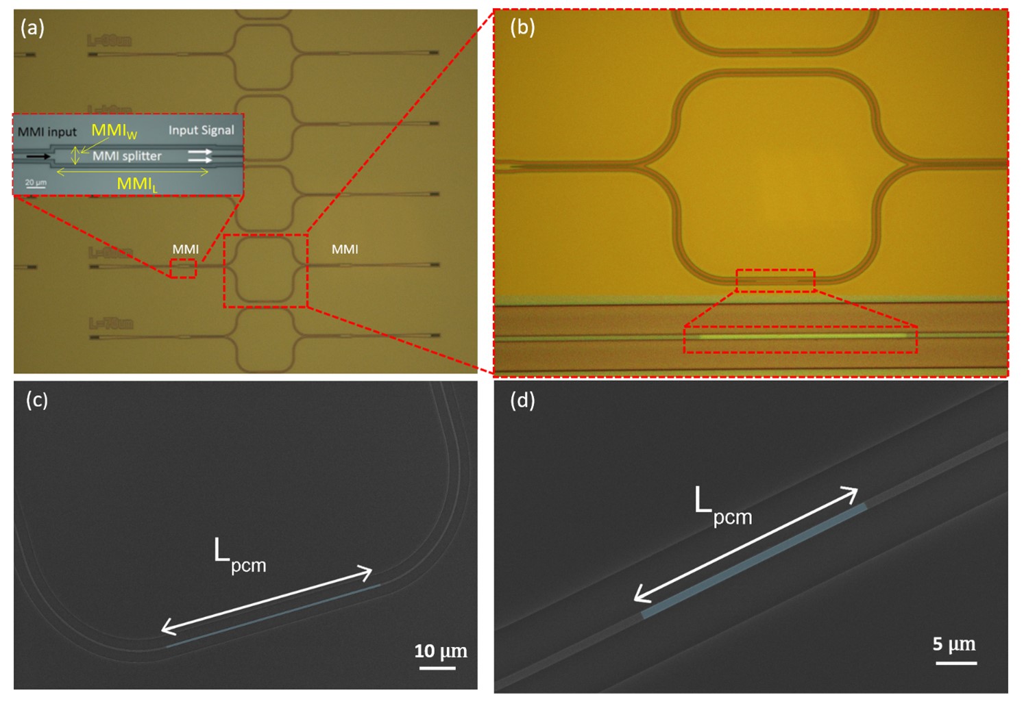
The layout we designed included a set of 12 MZIs with single-mode waveguide cross-sections of for (C-band) and for (O-band). These MZIs have an optical path length difference of = at and = at between their arms, see Fig. 1(a). In the longer arm of the MZI, PCM cells with a thickness of for Sb2S3 and for Sb2Se3 and different lengths ranging from were deposited. To split and combine the light, broadband multi-mode interferometers (MMIs) were employed, see inset of Fig 1(a). The dimensions of the MMI at = , were MMIL = and MMIW = , and respectively for = , MMIL = and MMIW = . SEM images of the longer MZI arm were taken with different lengths of the PCM cell. In Figure 1(c), a cell length of a was captured and in Fig. 1(d) a zoom in image of the longer arm with a cell length of was measured. All the devices included input and output grating couplers (GCs) designed to couple the light at either of both wavelengths of interest for characterisation, r . The GCs designed for consisted of a x surface grating with a period of tapered down to a single-mode waveguide width of , whereas the ones designed for had a surface grating with the same dimensions and a period of tapered to a single-mode width of . The angle between the optical fibers delivering light and the gratings was selected to be or to the normal to ensure maximum coupling at r , respectively. Additionally, the layout included separate structures with two GCs connected back-to-back for normalisation purposes. The spectral response for all the devices was characterised using two different tunable laser sources. An Agilent 8163B Lightwave Multimeter for the response at and a similar Agilent 8164B Lightwave Measurement System for the response at . The measurements were first performed for the amorphous state of the PCMs and then for their crystalline state. The phase change was induced thermally by heating the chip on a hot plate at the crystallisation temperature for 10 minutes. In both cases, the polarization of the light was controlled to ensure that only TE modes could propagate through the devices and the measurements were normalized to extract the loss contribution of the grating couplers.
3 Results and discussion
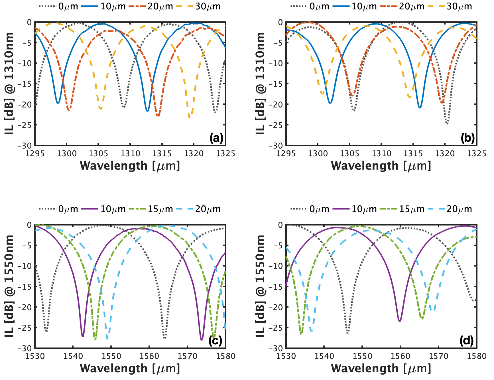
Silicon nitride MZIs were fabricated using novel low loss phase change materials, Sb2S3 and Sb2Se3 to demonstrate a low-loss non-volatile MZI building block for future electro-refractive non-volatile photonic integrated circuit applications in the O and C-bands. Firstly, the Sb2S3 material is analysed. The bare MZI structure without phase change material was characterized and normalized with respect to GCs connected back-to-back. Afterwards, the response of the MZIs for different lengths of the PCM cell were characterized in both amorphous (Fig. 2(a) and (c)) and crystalline states (Fig. 2(b) and (d)) at both target wavelengths.
In Fig. 2(a), the bare MZI presents a free-spectral range (FSR) of in the O-band. Only cell lengths of 10, 20 and were selected to be plotted in order to not overload the graph with all the cell lengths used in the study. The shift in wavelength () produced by the cell lengths were 2.75, 4.38 and respectively in the amorphous state respect to the bare MZI. In Fig. 2(b), the crystalline state is shown in the O-band. For the bare structure after crystallization, the FSR maintained the previous value (prior to crystallization), even though a shift has been produced in the dips of the optical spectrum due to the crystallization process to which the chip was submitted. In this case, a shift in wavelength for the cells of length 10, 20 and of 7.64, 9.5 and , respectively, was measured.
In each case, an extinction ratio (ER) higher than is shown for the different MZI structures. Fig 2(c) represents the MZI response using Sb2S3 in the amorphous state of the PCM in the C-band. A FSR of was extracted, higher than the one measured in the O-band (), a shift in wavelength for cell lengths of 10, 15 and of 9.67, 12.76 and was experimentally demonstrated. In Fig 2(d), the crystalline state of the PCM for the C-band is shown and shifts of 13.5, 19.5 and were obtained for the three different cell lengths, 10, 15 and . ERs as high as were experimentally demonstrated in this range of the spectrum, achieving a difference of 7.64, 9.5 and for the O-band and respectively 3.83, 6.74 and for the C-band between crystalline and amorphous dips.
Afterwards, we characterized the insertion loss (IL) introduced by the PCM layer () and the modulation in effective refractive index () in its amorphous and crystalline states. The IL and the modulation in phase were extracted from the spectral response of the fabricated MZIs. To characterize the losses of the PCM cell, the ER of each individual MZI with the corresponding cell length was evaluated and consequently the loss coefficient extracted using the equation from Ref.[62]:
| (1) |
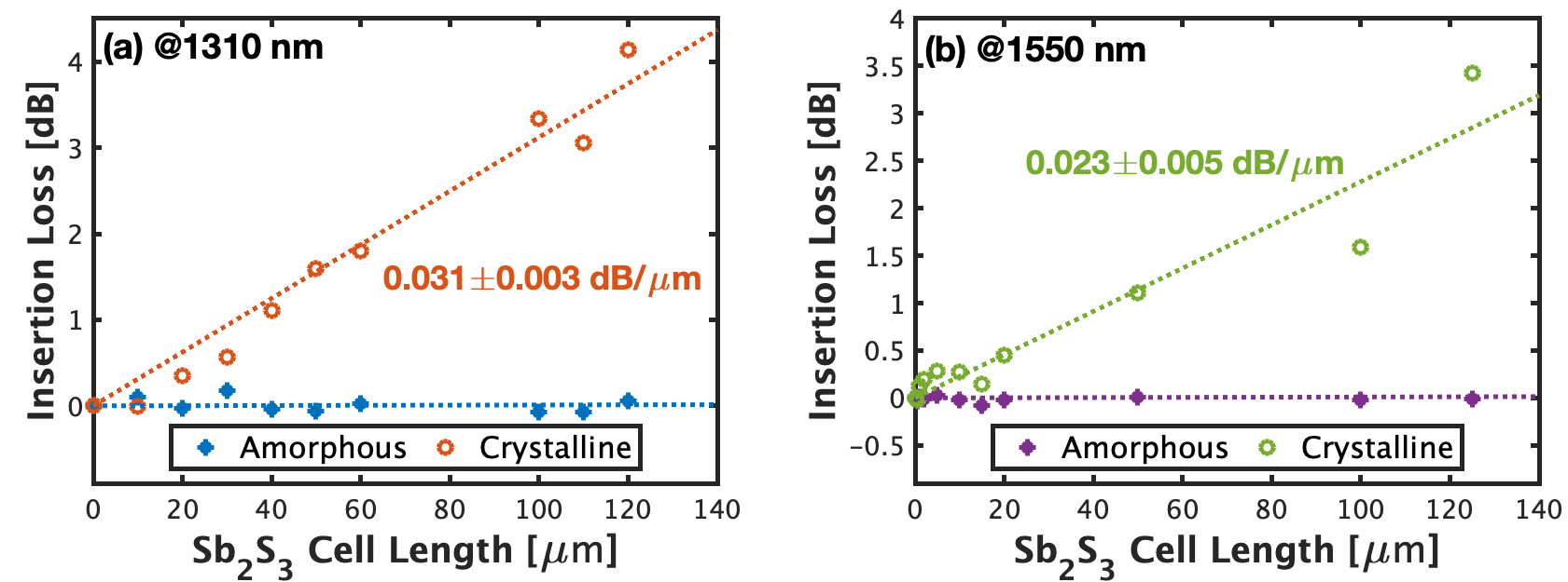
where is the length of the PCM cell. For the amorphous state of the PCM, the ER was not varying significantly while increasing the cell length, showing a low loss introduced by the PCM in both ranges of the spectrum. The extracted losses in the amorphous state for the wavelengths of interest are lower than . For the crystalline state, ERs were decreasing with increasing the cell lengths, showing an increment in losses in the crystalline state respect to the amorphous state. The measured IL in the crystalline state, were as low as and at 1310 nm and respectively, see Fig. 3.

Once the IL of the PCM was characterized, the effective refractive index modulation of the material can be obtained using the equation from Ref.[63]:
| (2) |
where is the variation produced in the effective refractive index when the PCM cell is introduced compared to the bare structure (no PCM), the superscripts and refer to the amorphous and crystalline states respectively, FSR is the free spectral range as previously introduced, and is the shift in the dip of the amorphous and crystalline states with respect to the dip produced by the bare MZI waveguide as introduced previously. Figure 4 shows the for both ranges of the spectrum, (Fig. 4(a)) and (Fig. 4(b)). The modulation between the amorphous state and the bare waveguide, the crystalline state and the bare waveguide and the amorphous state compared with the crystalline state () are presented in Fig. 4. The overall effective refractive index contrast between amorphous and crystalline states was measured to be 0.05 and 0.02 at and , respectively.
The same procedure was used in order to characterize the building block performance of the MZIs devices for the material, Sb2Se3. In this case, the spectral response for the different MZIs is presented in Fig. 5. Fig 5(a) shows the amorphous state of the Sb2Se3 material in the O-band. A shift of 9, 15.5 and between the bare MZI dip and the MZI dip with PCM cells of 10, 20 and was measured respectively. For the crystalline state, an increase in the shift is produced compared with the amorphous state and a shift of 13, 17.9 and is measured for cell lengths of 10, 20 and respectively. In all the cases ERs higher than 20 dB were demonstrated, see Fig. 5(b). In the C-band, the Sb2Se3 material showed a modulation in wavelength of 10.3, 17.5 and for PCM amorphous cell lengths of 5, 10 and . When switching to crystalline state, the modulation is 14.9, 30.65 and respectively, see Fig. 5(c-d). Resulting in a of 4, 2.1 and for O-band and respectively 4.6, 13.15 and for the C-band.

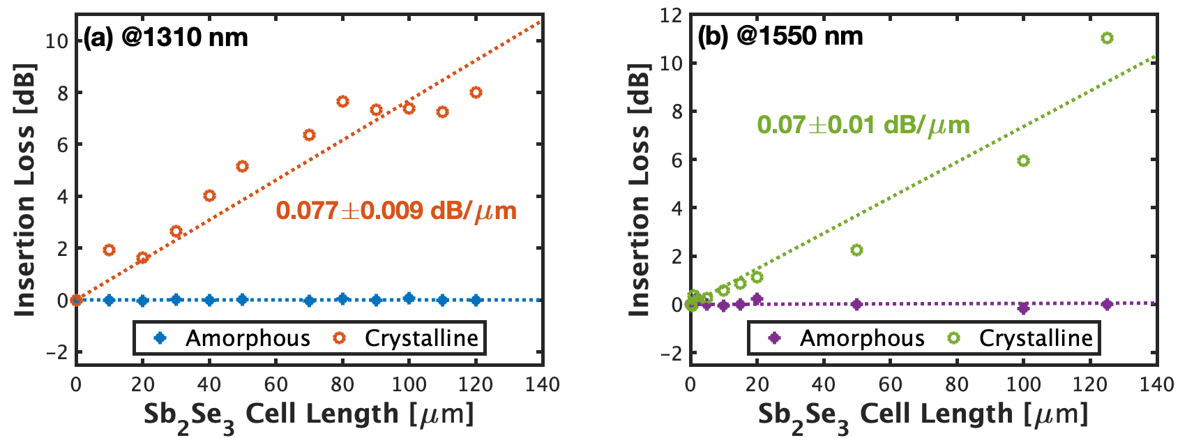

The ILs and the effective index modulation were extracted using the same method used for the Sb2S3 material. In this case, the measured losses in both states are shown in Fig. 6. In the amorphous state of Sb2Se3 for the wavelengths of interest, losses are lower than , whereas in the crystalline state, losses are at and at . The effective refractive index difference between the amorphous and crystalline state was measured to be 0.03 at and 0.05 at as shown in Fig. 7.
Table 1 presents the optical performance of the currently popular phase change materials GST, GSST and the novel materials discussed in this paper, Sb2S3 and Sb2Se3 on our integrated silicon nitride platform. In the table, a comparison of the cell length required in order to achieve a shift () and the IL that this cell introduces in the device are also shown. GST offers a phase shift at the shortest length while GSST requires double, Sb2Se3 triple and Sb2S3 seven times that length (the GST length) for the same shift at . However, the popularity of GSST stems from the three times lower insertion loss when compared to GST. Our Sb2Se3 and Sb2S3 films offer a stark improvement with the insertion loss at 13 and 18 times lower than GST respectively, significantly surpassing the benefits of GSST. In the O-band (), the required length for a shift () in the case of Sb2Se3 is , although, there is a reduction of for GST, for GSST and for the Sb2S3 material. Again in this range of the spectrum the IL introduced by the novel materials highly improve the performance of GST and GSST. It is therefore obvious that both materials provide in the O band and C band an incontestable improvement on insertion losses compared with GST and GSST in the crystalline state.
4 CONCLUSIONS
In this paper, a MZI building block is demonstrated exploiting a novel family of low loss phase change materials in the telecommunications O and C-bands for future non-volatile electro-refractive modulation in programmable photonic integrated circuits in mid index waveguides. Losses lower than for Sb2Se3 and for Sb2S3 are demonstrated in both ranges of the spectrum with changes in effective refractive index higher than 0.02. This study thus provides useful characterization information for the operation of non-volatile integrated photonic circuits based on phase change materials in two of the most important spectral ranges used for optical communications. The demonstration of these low loss non volatile building blocks, using a low loss and back end of the line compatible waveguide platform, have opened up pathways for more complex PIC’s architecture and extended applications.
Funding
Horizon 2020 Framework Programme (871391); Engineering and Physical Sciences Research Council (EP/M015130/1, EP/T007303/1, EP/R003076/1, EP/N00762X/1).
Disclosures
The authors declare no conflicts of interest.
References
- [1] X. Chen, M. M. Milosevic, S. Stanković, S. Reynolds, T. D. Bucio, K. Li, D. J. Thomson, F. Gardes, and G. T. Reed, “The emergence of silicon photonics as a flexible technology platform,” \JournalTitleProceedings of the IEEE 106, 2101–2116 (2018).
- [2] M. Smit, K. Williams, and J. Van Der Tol, “Past, present, and future of inp-based photonic integration,” \JournalTitleAPL Photonics 4, 050901 (2019).
- [3] S. Khan, J. Chiles, J. Ma, and S. Fathpour, “Silicon-on-nitride waveguides for mid-and near-infrared integrated photonics,” \JournalTitleApplied physics letters 102, 121104 (2013).
- [4] J. Hong, A. M. Spring, F. Qiu, and S. Yokoyama, “A high efficiency silicon nitride waveguide grating coupler with a multilayer bottom reflector,” \JournalTitleScientific reports 9, 1–8 (2019).
- [5] A. Brimont, D. Thomson, P. Sanchis, J. Herrera, F. Gardes, J. Fedeli, G. Reed, and J. Martí, “High speed silicon electro-optical modulators enhanced via slow light propagation,” \JournalTitleOptics Express 19, 20876–20885 (2011).
- [6] D. J. Thomson, F. Y. Gardes, J. M. Fedeli, S. Zlatanovic, Y. Hu, B. P. P. Kuo, E. Myslivets, N. Alic, S. Radic, G. Z. Mashanovich, and G. T. Reed, “50-Gb/s silicon optical modulator,” \JournalTitleIEEE Photonics Technology Letters 24, 234–236 (2012).
- [7] J. Faneca, B. T. Hogan, I. R. Diez, F. Y. Gardes, and A. Baldycheva, “Tuning silicon-rich nitride microring resonances with graphene capacitors for high-performance computing applications,” \JournalTitleOptics Express 27, 35129–35140 (2019).
- [8] Y.-Q. Bie, G. Grosso, M. Heuck, M. M. Furchi, Y. Cao, J. Zheng, D. Bunandar, E. Navarro-Moratalla, L. Zhou, D. K. Efetov et al., “A mote 2-based light-emitting diode and photodetector for silicon photonic integrated circuits,” \JournalTitleNature nanotechnology 12, 1124–1129 (2017).
- [9] F. Xia, T. Mueller, Y.-m. Lin, A. Valdes-Garcia, and P. Avouris, “Ultrafast graphene photodetector,” \JournalTitleNature nanotechnology 4, 839–843 (2009).
- [10] Z. Zhou, B. Yin, and J. Michel, “On-chip light sources for silicon photonics,” \JournalTitleLight: Science & Applications 4, e358 (2015).
- [11] D. A. Miller, “Silicon photonics: Meshing optics with applications,” \JournalTitleNature Photonics 11, 403–404 (2017).
- [12] L. Chrostowski, H. Shoman, M. Hammood, H. Yun, J. Jhoja, E. Luan, S. Lin, A. Mistry, D. Witt, N. A. Jaeger et al., “Silicon photonic circuit design using rapid prototyping foundry process design kits,” \JournalTitleIEEE Journal of Selected Topics in Quantum Electronics 25, 1–26 (2019).
- [13] W. Bogaerts and L. Chrostowski, “Silicon photonics circuit design: methods, tools and challenges,” \JournalTitleLaser & Photonics Reviews 12, 1700237 (2018).
- [14] W. Bogaerts, D. Pérez, J. Capmany, D. A. Miller, J. Poon, D. Englund, F. Morichetti, and A. Melloni, “Programmable photonic circuits,” \JournalTitleNature 586, 207–216 (2020).
- [15] K. E. Zinoviev, A. B. González-Guerrero, C. Domínguez, and L. M. Lechuga, “Integrated bimodal waveguide interferometric biosensor for label-free analysis,” \JournalTitleJournal of lightwave technology 29, 1926–1930 (2011).
- [16] R. Wang, A. Vasiliev, M. Muneeb, A. Malik, S. Sprengel, G. Boehm, M.-C. Amann, I. Šimonytė, A. Vizbaras, K. Vizbaras et al., “Iii–v-on-silicon photonic integrated circuits for spectroscopic sensing in the 2–4 m wavelength range,” \JournalTitleSensors 17, 1788 (2017).
- [17] C. Oton, C. Manganelli, F. Bontempi, M. Fournier, D. Fowler, and C. Kopp, “Silicon photonic waveguide metrology using mach-zehnder interferometers,” \JournalTitleOptics express 24, 6265–6270 (2016).
- [18] D. Pérez, I. Gasulla, L. Crudgington, D. J. Thomson, A. Z. Khokhar, K. Li, W. Cao, G. Z. Mashanovich, and J. Capmany, “Multipurpose silicon photonics signal processor core,” \JournalTitleNature communications 8, 1–9 (2017).
- [19] D. Pérez, I. Gasulla, P. D. Mahapatra, and J. Capmany, “Principles, fundamentals, and applications of programmable integrated photonics,” \JournalTitleAdvances in Optics and Photonics 12, 709–786 (2020).
- [20] T. Rudolph, “Why i am optimistic about the silicon-photonic route to quantum computing,” \JournalTitleAPL Photonics 2, 030901 (2017).
- [21] X. Qiang, X. Zhou, J. Wang, C. M. Wilkes, T. Loke, S. O’Gara, L. Kling, G. D. Marshall, R. Santagati, T. C. Ralph et al., “Large-scale silicon quantum photonics implementing arbitrary two-qubit processing,” \JournalTitleNature photonics 12, 534–539 (2018).
- [22] S. Nandakumar, M. Le Gallo, I. Boybat, B. Rajendran, A. Sebastian, and E. Eleftheriou, “A phase-change memory model for neuromorphic computing,” \JournalTitleJournal of Applied Physics 124, 152135 (2018).
- [23] I. Boybat, M. Le Gallo, S. Nandakumar, T. Moraitis, T. Parnell, T. Tuma, B. Rajendran, Y. Leblebici, A. Sebastian, and E. Eleftheriou, “Neuromorphic computing with multi-memristive synapses,” \JournalTitleNature communications 9, 1–12 (2018).
- [24] T. H. Szymanski, “Securing the industrial-tactile internet of things with deterministic silicon photonics switches,” \JournalTitleIEEE Access 4, 8236–8249 (2016).
- [25] Y. Zhou, S. Zheng, Z. Liu, T. Wen, Z. Ding, J. Yan, and G. Zhang, “Passive and active phase change materials integrated building energy systems with advanced machine-learning based climate-adaptive designs, intelligent operations, uncertainty-based analysis and optimisations: A state-of-the-art review,” \JournalTitleRenewable and Sustainable Energy Reviews 130, 109889 (2020).
- [26] A. Rahim, E. Ryckeboer, A. Z. Subramanian, S. Clemmen, B. Kuyken, A. Dhakal, A. Raza, A. Hermans, M. Muneeb, S. Dhoore et al., “Expanding the silicon photonics portfolio with silicon nitride photonic integrated circuits,” \JournalTitleJournal of lightwave technology 35, 639–649 (2017).
- [27] P. P. Absil, P. Verheyen, P. De Heyn, M. Pantouvaki, G. Lepage, J. De Coster, and J. Van Campenhout, “Silicon photonics integrated circuits: a manufacturing platform for high density, low power optical i/o’s,” \JournalTitleOptics express 23, 9369–9378 (2015).
- [28] J. Klamkin, H. Zhao, B. Song, Y. Liu, B. Isaac, S. Pinna, F. Sang, and L. Coldren, “Indium phosphide photonic integrated circuits: Technology and applications,” in 2018 IEEE BiCMOS and Compound Semiconductor Integrated Circuits and Technology Symposium (BCICTS), (IEEE, 2018), pp. 8–13.
- [29] H. Zhao, S. Pinna, F. Sang, B. Song, S. T. Š. Brunelli, L. A. Coldren, and J. Klamkin, “High-power indium phosphide photonic integrated circuits,” \JournalTitleIEEE Journal of Selected Topics in Quantum Electronics 25, 1–10 (2019).
- [30] T. Domínguez Bucio, C. Lacava, M. Clementi, J. Faneca, I. Skandalos, A. Baldycheva, M. Galli, K. Debnath, P. Petropoulos, and F. Gardes, “Silicon Nitride Photonics for the Near-Infrared,” \JournalTitleIEEE Journal of Selected Topics in Quantum Electronics 26, 1–13 (2019).
- [31] T. Domínguez Bucio, A. Z. Khokhar, G. Z. Mashanovich, and F. Y. Gardes, “N-rich silicon nitride angled MMI for coarse wavelength division (de)multiplexing in the O-band,” \JournalTitleOptics Letters 43, 1251 (2018).
- [32] J. N. Milgram, J. Wojcik, P. Mascher, and a. P. Knights, “Optically pumped Si nanocrystal emitter integrated with low loss silicon nitride waveguides.” \JournalTitleOptics express 15, 14679–14688 (2007).
- [33] S. Gaugiran, S. Gétin, J. M. Fedeli, G. Colas, A. Fuchs, F. Chatelain, and J. Dérouard, “Optical manipulation of microparticles and cells on silicon nitride waveguides,” \JournalTitleOptics Express 13, 6956 (2005).
- [34] R. Baets, A. Z. Subramanian, S. Clemmen, B. Kuyken, P. Bienstman, N. Le Thomas, G. Roelkens, D. Van Thourhout, P. Helin, and S. Severi, “Silicon photonics: silicon nitride versus silicon-on-insulator,” in Optical Fiber Communication Conference, (Optical Society of America, 2016), pp. Th3J–1.
- [35] X. Li, N. Youngblood, Z. Cheng, S. G.-C. Carrillo, E. Gemo, W. H. Pernice, C. D. Wright, and H. Bhaskaran, “Experimental investigation of silicon and silicon nitride platforms for phase-change photonic in-memory computing,” \JournalTitleOptica 7, 218–225 (2020).
- [36] C. Rios, M. Stegmaier, Z. Cheng, N. Youngblood, C. D. Wright, W. H. Pernice, and H. Bhaskaran, “Controlled switching of phase-change materials by evanescent-field coupling in integrated photonics,” \JournalTitleOptical Materials Express 8, 2455–2470 (2018).
- [37] M. Wuttig, H. Bhaskaran, and T. Taubner, “Phase-change materials for non-volatile photonic applications,” \JournalTitleNature Photonics 11, 465 (2017).
- [38] M. Wuttig and N. Yamada, “Phase-change materials for rewriteable data storage,” \JournalTitleNature materials 6, 824–832 (2007).
- [39] R. Soref, “Tutorial: Integrated-photonic switching structures,” \JournalTitleApl Photonics 3, 021101 (2018).
- [40] G. Bruns, P. Merkelbach, C. Schlockermann, M. Salinga, M. Wuttig, T. Happ, J. Philipp, and M. Kund, “Nanosecond switching in GeTe phase change memory cells,” \JournalTitleApplied physics letters 95, 043108 (2009).
- [41] N. Ciocchini, M. Laudato, M. Boniardi, E. Varesi, P. Fantini, A. L. Lacaita, and D. Ielmini, “Bipolar switching in chalcogenide phase change memory,” \JournalTitleScientific reports 6, 29162 (2016).
- [42] P. Li, X. Yang, T. W. Maß, J. Hanss, M. Lewin, A.-K. U. Michel, M. Wuttig, and T. Taubner, “Reversible optical switching of highly confined phonon–polaritons with an ultrathin phase-change material,” \JournalTitleNature materials 15, 870–875 (2016).
- [43] H. Y. Cheng, T. H. Hsu, S. Raoux, J. Y. Wu, P. Y. Du, M. Breitwisch, Y. Zhu, E. K. Lai, E. Joseph, S. Mittal, R. Cheek, A. Schrott, S. C. Lai, H. L. Lung, and C. Lam, “A high performance phase change memory with fast switching speed and high temperature retention by engineering the gexsbytez phase change material,” in 2011 International Electron Devices Meeting, (2011), pp. 3.4.1–3.4.4.
- [44] M. Stegmaier, C. Ríos, H. Bhaskaran, C. D. Wright, and W. H. Pernice, “Nonvolatile all-optical 1x2 switch for chipscale photonic networks,” \JournalTitleAdvanced Optical Materials 5, 1600346 (2017).
- [45] F. De Leonardis, R. Soref, V. M. Passaro, Y. Zhang, and J. Hu, “Broadband electro-optical crossbar switches using low-loss ge 2 sb 2 se 4 te 1 phase change material,” \JournalTitleJournal of Lightwave Technology 37, 3183–3191 (2019).
- [46] J. Feldmann, N. Youngblood, X. Li, C. D. Wright, H. Bhaskaran, and W. H. Pernice, “Integrated 256 cell photonic phase-change memory with 512-bit capacity,” \JournalTitleIEEE Journal of Selected Topics in Quantum Electronics 26, 1–7 (2019).
- [47] P. Xu, J. Zheng, J. K. Doylend, and A. Majumdar, “Low-loss and broadband nonvolatile phase-change directional coupler switches,” \JournalTitleACS Photonics 6, 553–557 (2019).
- [48] C. Ríos, M. Stegmaier, P. Hosseini, D. Wang, T. Scherer, C. D. Wright, H. Bhaskaran, and W. H. Pernice, “Integrated all-photonic non-volatile multi-level memory,” \JournalTitleNature Photonics 9, 725 (2015).
- [49] N. Farmakidis, N. Youngblood, X. Li, J. Tan, J. L. Swett, Z. Cheng, C. D. Wright, W. H. Pernice, and H. Bhaskaran, “Plasmonic nanogap enhanced phase-change devices with dual electrical-optical functionality,” \JournalTitleScience Advances 5, eaaw2687 (2019).
- [50] E. Gemo, S. G.-C. Carrillo, C. R. De Galarreta, A. Baldycheva, H. Hayat, N. Youngblood, H. Bhaskaran, W. H. Pernice, and C. D. Wright, “Plasmonically-enhanced all-optical integrated phase-change memory,” \JournalTitleOptics express 27, 24724–24737 (2019).
- [51] Z. Cheng, C. Ríos, W. H. Pernice, C. D. Wright, and H. Bhaskaran, “On-chip photonic synapse,” \JournalTitleScience advances 3, e1700160 (2017).
- [52] J. Feldmann, N. Youngblood, C. Wright, H. Bhaskaran, and W. Pernice, “All-optical spiking neurosynaptic networks with self-learning capabilities,” \JournalTitleNature 569, 208–214 (2019).
- [53] J. Faneca, S. G.-C. Carrillo, E. Gemo, C. R. de Galarreta, T. D. Bucio, F. Y. Gardes, H. Bhaskaran, W. H. Pernice, C. D. Wright, and A. Baldycheva, “Performance characteristics of phase-change integrated silicon nitride photonic devices in the o and c telecommunications bands,” \JournalTitleOptical Materials Express 10, 1778–1791 (2020).
- [54] Y. Zhang, J. Li, J. Chou, Z. Fang, A. Yadav, H. Lin, Q. Du, J. Michon, Z. Han, Y. Huang et al., “Broadband transparent optical phase change materials,” in CLEO: Applications and Technology, (Optical Society of America, 2017), pp. JTh5C–4.
- [55] M. Miscuglio, J. Meng, O. Yesiliurt, Y. Zhang, L. J. Prokopeva, A. Mehrabian, J. Hu, A. V. Kildishev, and V. J. Sorger, “Artificial synapse with mnemonic functionality using gsst-based photonic integrated memory,” in 2020 International Applied Computational Electromagnetics Society Symposium (ACES), (IEEE, 2020), pp. 1–3.
- [56] Y. Zhang, J. B. Chou, J. Li, H. Li, Q. Du, A. Yadav, S. Zhou, M. Y. Shalaginov, Z. Fang, H. Zhong et al., “Broadband transparent optical phase change materials for high-performance nonvolatile photonics,” \JournalTitleNature communications 10, 1–9 (2019).
- [57] W. Dong, H. Liu, J. K. Behera, L. Lu, R. J. Ng, K. V. Sreekanth, X. Zhou, J. K. Yang, and R. E. Simpson, “Wide bandgap phase change material tuned visible photonics,” \JournalTitleAdvanced Functional Materials 29, 1806181 (2019).
- [58] M. Delaney, I. Zeimpekis, D. Lawson, D. W. Hewak, and O. L. Muskens, “A new family of ultralow loss reversible phase-change materials for photonic integrated circuits: Sb2s3 and sb2se3,” \JournalTitleAdvanced Functional Materials 30, 2002447 (2020).
- [59] J. Faneca, L. Trimby, I. Zeimpekis, M. Delaney, D. W. Hewak, F. Y. Gardes, C. D. Wright, and A. Baldycheva, “On-chip sub-wavelength bragg grating design based on novel low loss phase-change materials,” \JournalTitleOptics Express 28, 16394–16406 (2020).
- [60] Z. Fang, J. Zheng, and A. Majumdar, “Non-volatile integrated photonics enabled by broadband transparent phase change material,” in CLEO: Applications and Technology, (Optical Society of America, 2020), pp. JTh2B–3.
- [61] T. Domínguez Bucio, A. Z. Khokhar, C. Lacava, S. Stankovic, G. Z. Mashanovich, P. Petropoulos, and F. Y. Gardes, “Material and optical properties of low-temperature NH3-free PECVD SiNx layers for photonic applications,” \JournalTitleJournal of Physics D: Applied Physics 50 (2017).
- [62] C. Rios, P. Hosseini, C. D. Wright, H. Bhaskaran, and W. H. Pernice, “On-chip photonic memory elements employing phase-change materials,” \JournalTitleAdvanced Materials 26, 1372–1377 (2014).
- [63] H. Zhang, L. Zhou, B. M. A. Rahman, X. Wu, L. Lu, Y. Xu, J. Xu, J. Song, Z. Hu, L. Xu, and J. Chen, “Ultracompact si-gst hybrid waveguides for nonvolatile light wave manipulation,” \JournalTitleIEEE Photonics Journal 10, 1–10 (2018).