Strongly non-linear superconducting silicon resonators
Abstract
Superconducting boron-doped silicon is a promising material for integrated silicon quantum devices. In particular, its low electronic density and moderate disorder make it a suitable candidate for the fabrication of large inductances with low losses at microwave frequencies. We study experimentally the electrodynamics of superconducting silicon thin layers using coplanar waveguide resonators, focusing on the kinetic inductance, the internal losses, and the variation of these quantities with the resonator read-out power. We report the first observation in a doped semiconductor of microwave resonances with internal quality factors of a few thousand. As expected in the BCS framework, superconducting silicon presents a large sheet kinetic inductance in the 50-500 pH range, comparable to strongly disordered superconductors. The kinetic inductance temperature dependence is well described by Mattis-Bardeen theory. However, we find an unexpectedly strong non-linearity of the complex surface impedance that cannot be satisfyingly explained either by depairing or by quasiparticle heating.
I Introduction
Lossless high-inductance microwave components made from superconducting materials are currently under intense study, both theoretically and experimentally, as they play a crucial role in cavity QED Samkharadze et al. (2016); Kuzmin et al. (2019); Léger et al. (2019), in protecting qubits from their electromagnetic environment Manucharyan et al. (2009), in fast two-qubit gates Harvey et al. (2018), and in sensitive astronomical detectors Day et al. (2003); Barends et al. (2007); Zmuidzinas (2012). The development of such components made from superconducting silicon would be of particular interest for silicon-based quantum electronics, initiated with the demonstration of CMOS silicon spin qubits Maurand et al. (2016). Silicon becomes a superconductor when a few percent of the silicon atoms are replaced by boron Bustarret et al. (2006). Using a pulsed laser doping technique, layers of superconducting silicon ultra-doped with boron (Si:B) can be fabricated with controlled thickness and dopant concentration. This control allows, in turn, to tune the superconducting critical temperature in the - range Marcenat et al. (2010); Bhaduri et al. (2012); Grockowiak et al. (2013). However, while the DC properties of such tunable BCS superconductor are now well understood, little is known about its surface impedance at the microwave frequencies that are relevant for quantum information applications. The surface impedance of thin-film superconductors is often dominated by the kinetic inductance , due to the inertia of the Cooper-pair condensate. Indeed, is proportional to the ratio of the normal-state sheet resistance just above and the superconducting gap energy . Disordered superconductors and very thin films of elemental superconductors may then have such high that the kinetic inductance strongly exceeds the "geometrical" inductance due to energy storage in the magnetic field.
Here, we report the first observation in a superconducting doped semiconductor of microwave resonances with internal quality factors of a few thousand. We show that the kinetic inductance of our thin Si:B films is large, and comparable to strongly disordered superconductors such as TiN Swenson et al. (2013); Leduc et al. (2010); Shearrow et al. (2018), NbN Annunziata et al. (2010); Niepce et al. (2019); Gao et al. (2007), NbTi McCambridge (1995), NbSi Calvo et al. (2014), W Basset et al. (2019) and granular Al Maleeva et al. (2018). Si:B kinetic inductance measurements match the predictions based on DC measurements of and , where / is large due to the low carrier density and moderate disorder in the doped semiconductor. We show that the temperature and frequency dependence of the kinetic inductance also follow the predictions of the BCS-based Mattis-Bardeen equations. However, the non-linearity, manifested by the increases in both kinetic inductance and internal dissipation with increasing read-out power, is unexpectedly large, and cannot be fully explained as either depairing Semenov et al. (2016) or quasiparticle heating Guruswamy et al. (2015).
II Epitaxial superconducting silicon
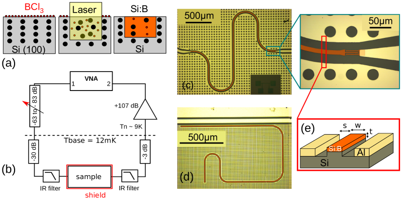
Silicon strongly doped with boron is a type II disordered BCS superconductor Bustarret et al. (2006) with a critical temperature that increases with increasing boron concentration up to Grockowiak et al. (2013); Dahlem et al. (2010). A nonequilibrium doping technique is necessary to create a superconductor because the minimal boron concentration required Grockowiak et al. (2013) is about three times the solubility limit Murrell et al. (2000). For this purpose, we use gas immersion laser doping (GILD) Débarre et al. (2002), whose principle is shown in Fig. 1a and in Methods. The GILD technique turns the silicon substrate, over a thickness , into epitaxial layers with a tunable boron concentration up to 10 at. (), without the formation of boron aggregates Hoummada et al. (2012). The layers are homogeneously doped in thickness except for a few nanometer metallic layer at the interface between the Si and Si:B, over which the doping drops to 0. The laser intensity has spatial inhomogeneities , which result in spatial fluctuations of the layer thickness, and may also result in small fluctuations of the critical temperature.
The resonators described in this work are patterned from Si:B layers epitaxied on a high-resistivity () Si substrate. These layers have surface area, thickness from and boron concentration 4 to (8 to 9.5 at.). The layers have a critical temperature from , a maximum transition width and a sheet resistance from , corresponding to resistivities . The layer thickness is much larger than the electronic mean free path , and is comparable or smaller than the superconducting coherence length . These parameters, for all the resonators investigated here (labeled from A to I), are summarized in Table 1 together with their geometrical and electrical properties.
![[Uncaptioned image]](/html/2101.11125/assets/x2.png)
III Silicon resonator design and fabrication
Our superconducting coplanar waveguide (CPW) resonators are fabricated as follows: first, the central conductor is patterned in a Si:B layer by optical lithography and a fluorine-based reactive ion etch; then, the ground planes and leads are patterned via lift-off from a evaporated Al film. The ground plane thickness is comparable to the etched depth around the Si:B line. The use of Al allows (i) keeping a constant impedance matching of our samples to the microwave equipment regardless of the Si:B surface impedance, and (ii) simplifying the system under study to a single conductor, allowing a more accurate extraction of the kinetic inductance value Gao (2008). The Al ground plane in the vicinity of the resonator contains a grid of wide holes acting as magnetic flux traps to limit the dissipation due to vortex motion Stan et al. (2004) (Fig. 1c,d).
We characterize both half-wave () and quarter-wave () resonators. The half-wave resonators are coupled at both ends to on-chip Al transmission lines via small capacitances. These resonators are measured in a transmission configuration: the measured signal propagates through the resonator (Fig. 1c). The quarter-wave resonators are coupled at their open end to a transmission line, while their opposite end is shorted to the Al ground plane. These resonators are measured in a shunt configuration, meaning that the measured signal is the complex sum of the signal propagating past the resonator and the signal radiated from it in the forward direction (Fig. 1d). The latter geometry is best suited for reading out several resonators with different resonance frequencies in a single run. In our samples, the transmission line crosses three laser-doped spots each containing one resonator. Four-wire DC measurements were performed in parallel on laser doped samples fabricated at the same time.
The design of the resonators was determined by adjusting with microwave simulations in SONNET software the resonance frequencies and coupling loss rates (see Methods). To achieve an accurate determination of the resonators’ internal loss rates , we target values of the coupling losses near the critical coupling . is in the range s-1, corresponding to quality factors 2000 to 46000, while s-1 corresponds to quality factors 150 to 4000. (See Table 1).
IV Measurement setup and linear response
We use conventional microwave spectroscopy measurements of the superconducting Si:B resonators to determine the kinetic inductance of the film, the resonator internal loss rates and the amount of non-linearity in both of these quantities. We extract these values from measurements of the complex forward scattering parameter at frequencies from , at temperatures from , and using power levels at the sample input that range from . At resonance, the photon number in the resonator is where is the total loss rate, and varies from less than 1 to a few million for the power levels used here. As shown in Fig. 1b, both input and output lines are shielded to prevent significantly populating the resonators with thermal photons.
The measured is the product of the signal of interest transmitted through the chip and the background transmission due to the input and output lines. In the shunt configuration, the background transmission can be measured in the normal state of Si:B, while the Al is in the superconducting state. This compromise is best achieved around , where no Si:B resonance can be detected, and where the background transmission is almost independent of the temperature. In the transmission configuration, the background was estimated in a separate run. With this background removed, the transmission coefficient used to fit data in the shunt configuration is
| (1) |
while in the transmission configuration it is
| (2) |
where is the detuning. The asymmetry and leakage account for on-chip imperfections: is nonzero when the field radiated from the resonator reflects off an impedance mismatch such as that occurring at the micro-bonding connections Khalil et al. (2012); Megrant et al. (2012), while is nonzero when the input signal couples directly to the output.
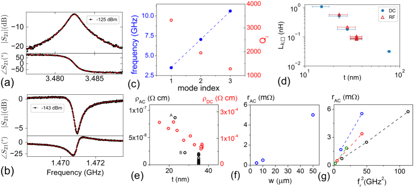
The linear response is measured with a minimum applied power corresponding to a few photons on average in the resonator, where the curve is independent of the read-out power. The experimental data are fitted with Eq. (1) or Eq. (2) up to , where most resonances vanish in the noise. From these fits we extract , and as a function of temperature up to . Characteristic measurements with the corresponding fits are presented in Figs. 2a and b. As expected, our resonators are multi-modal, with resonant frequencies scaling with the mode number as for half-wave resonators and as for quarter-wave resonators. In our experimentally accessible frequency range we can thus observe the first two or three modes of each resonance.
V Low temperature kinetic inductance in the linear regime
In the BCS theory, the kinetic inductance at low temperature () and low frequency () is:
| (3) |
In the case where the inductance is so high that the current density is uniform, it is convenient to introduce the sheet kinetic inductance , as is done for the sheet resistance. This quantity is relevant in our experiments, where only the CPW resonator central conductor is made from Si:B, and has a small cross-section.
Using Eq. 3 with the sheet resistance and extracted from DC measurements, is found to be in the range for Si:B thicknesses ranging from . These values are then compared to those extracted from the RF measurements by adjusting the SONNET electromagnetic simulations to reproduce the measured resonance frequencies. Note that the values deduced from the SONNET simulations are found in good agreement with the analytical values obtained from the resonant frequency , for the first mode, where is the length of the resonator, for a () resonator, and , , and are respectively the capacitance, geometric inductance and kinetic inductance per unit length. This expression, where the current distribution (relatively homogeneous) in the width of the central conductor was taken into account (see Methods), is valid when the losses can be neglected. Fig. 2d shows excellent agreement between the values inferred from the high frequency measurements and those calculated from the DC characteristics, confirming the validity of the BCS description and suggesting that values of the order of could be obtained in Si:B resonators patterned from thinner layers. For all our samples, the kinetic inductance participation ratio ranges from 0.94 to 0.99. The resonator characteristic impedance lies in the range . In particular, the thick resonators, whose results are mainly shown here, have .
VI Low temperature losses in the linear regime
We evaluate the residual resistance at microwave frequency in the Si:B layer with a resonator effective RLC lumped-element model. As for the extraction of the sheet kinetic inductance from the resonance frequency, we aim at extracting the residual sheet resistance from the losses, describing our material independently of the device geometry. We compute the AC sheet resistance from the internal quality factor and sheet kinetic inductance with , with the base temperature, saturated, internal quality factor of the mode. This sheet resistance is reflective of the ohmic losses in the inductor and ranges from . We find that the AC losses depend on the layer thickness, as already observed for the DC resistivity (Fig. 2e): when the thickness decreases, both AC and DC Si:B resistivities (; ) increase as a result of a larger amount of interstitial boron and, correspondingly, of disorder Bonnet (2019) (see Methods). The highest are observed for the thinner, lossier, more disordered samples, which present the highest . Furthermore, strongly increases with the resonator width, as observed in Fig. 2f for samples C, D and I, whose laser doping and fabrication were realised at the same time, and that were probed by the same transmission line. Finally, is plotted against frequency in Fig. 2g, for the samples where multiple harmonics could be measured, and was shown to increase as . The frequency and width dependencies are in quantitative agreement with AC losses due to magnetic vortices, for which the motion of the non-superconducting vortex core leads to dissipation (see Methods). However, in a control experiment with extensive magnetic shielding on sample C the losses were not found to vary significantly. This could indicate that another type of vortex loss involving vortex-antivortex pairs is at play. Other features can also contribute to the observed losses. For instance, a few nanometer thick metallic layer is present at the Si:B/Si interface, where the dopant concentration decreases below the superconductivity threshold, and whose thickness depends on the layer properties. However the associated AC sheet resistance is not expected to depend on the conductor width. Further experiments are still needed to discriminate between the possible sources of loss.
VII Temperature dependence of resonant frequency and losses - Mattis-Bardeen theory
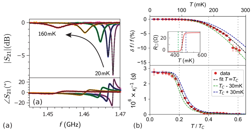
Fig. 3a shows a selection of the background-removed data measured in the linear response regime at several temperatures for sample C. A reduction of the resonant frequency and quality factor is observed, as the thermally-induced Cooper pair breaking increases the kinetic inductance and the losses Gao (2008). In Fig. 3b, we compare the characteristic temperature dependence of the relative frequency shift and inverse internal losses to the prediction of Mattis-Bardeen theory Mattis and Bardeen (1958), valid for homogeneous weak-coupled BCS superconductors with low or moderate disorder. The evaluation of the frequency-dependent complex conductivity is based on two input parameters extracted from DC measurements: and . Fig. 3b shows the good agreement obtained for the frequency shift, without any free parameters, up to temperatures as high as where decreases by 10. We add to Fig. 3b, to guide the eye, the Mattis-Bardeen expectations for and . Such temperature range roughly corresponds to the width of the superconducting transition of the sample, as shown in the inset of Fig. 3b. Above the determination of and becomes increasingly difficult due to the vanishing amplitude of the field coming out of the resonator (since ), and to the low read-out power required to remain in the linear regime. Despite the increased uncertainty, however, a small shift from the expected dependence can be observed above . This may be the result of some inhomogeneities in in the Si:B layer, as a gap dispersion of the order of was measured by scanning tunneling spectroscopy Dahlem et al. (2010).
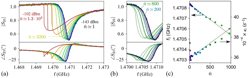
Fig. 3b shows the temperature dependence of the internal losses. At high temperature (), losses due to thermally activated quasiparticles are well-described by Mattis-Bardeen (). At the base temperature, is found to saturate due to additional loss mechanisms, giving a saturation value . The total internal losses are written . This saturation value takes into account all the usual non-thermal contributions, such as quasiparticles excited by unshielded radiation or by the read-out power, the dissipation due to two-level systems or by vortex motion, etc. In conclusion, the linear response of Si:B at finite frequency shows a good agreement with the BCS-based Mattis-Bardeen theory, at all temperatures for the purely reactive (inductive) response. At temperatures however, a loss mechanism, discussed when commenting the AC sheet resistance at the base temperature, takes over the dissipative response.
VIII Non-linearities of kinetic inductance and losses
The results shown up to now are characteristic of the linear regime. However, when increasing the readout power, the resonances shift towards the low frequencies, then become progressively skewed, up to a bistable state where an hysteresis is observed between frequency sweeps up and down (Fig. 4a). Alongside with this change of resonance frequency and shape, we also note an increase in the internal losses, with a reduction of the resonance amplitude. From a first qualitative point of view, in Si:B, this non-linearity appears at extremely low power: as an example, the first mode () of sample C undergoes frequency shifts of the order of at read-out powers of the order of fW, corresponding to about 200 photons in the resonator, while the hysteresis appears for pW powers. To describe quantitatively the resonance curves in the non-linear regime, the harmonic oscillator Hamiltonian characteristic of the linear regime is replaced by , where and are the photon creation and annihilation operators, and is the Kerr coefficient, quantifying the non-linear response. The energies of this oscillator are no longer equidistant, but acquire a Fock state dependent shift , where is the Fock index. In consequence, the measured resonance shifts with the average photon population writes Yurke and Buks (2006). Non-linear losses are also taken into account, introducing a loss term proportional to the number of photons and writing the total losses . The transmission coefficient, in the case of a shunt-coupled geometry finally reads
| (4) |
A similar expression is found in the transmission geometry. Fig.4b shows the results of the fits from Eq. (4), where the curves in the low power range, for both the up and down sweeps, are described by a single Kerr number and a single non-linear loss term . The other parameters in the fit, , , , and the asymmetry , are fixed at the linear regime values. All the curves measured in the wider power range, corresponding to photons in the resonators, are well-described by Eq. (4), but only the low-power curves, with can be described by a common and . This deviation may be due to higher order terms in the Hamiltonian. Henceforth, we will exclusively discuss the low-power non-linear parameters. Note that the low-power Kerr values and non-linear losses deduced from the non-linear fit are in good agreement, within 20, with the linear variation with of the resonant frequency and losses extracted from linear fits of for (see Fig. 4c).
The extracted and are reported in Table 1 for the measured harmonics of all resonators. The fits output a negative and a positive , consistent with the expectation that, whatever the non-linearity mechanism, it corresponds to a weakening of superconductivity and thus an increase of the kinetic inductance and additional losses in the system. The smallest Kerr numbers reported are, in absolute value, of the order of for macroscopic CPW structures, showing the extreme sensitivity of superconducting silicon to microwave power.
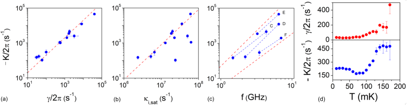
In Fig. 5 we plot the variation of the Kerr coefficient against the non-linear losses , the saturation losses in the linear regime , the frequency and the temperature. The non-linear inductive response () is associated to non-linear losses () over a broad range of magnitudes (Fig. 5a), with a ratio (dashed line and Table 1). At the base temperature, the non-linearity is higher for the samples presenting higher losses in the linear regime (Fig. 5b). and strongly depend on frequency, with (dotted lines in Fig. 5c) and , with . Finally, the temperature dependence of and is measured for two samples (C, shown in Fig. 5d, and F). The non-linearity globally increases with temperature. To explain the characterised non-linearity, we examine in detail the two most common sources of non-linearity in superconducting resonators: the non-linearity of the kinetic inductance induced by depairing, and the non-linearity induced by quasiparticle heating.
IX Modeling non-linearity with depairing
A non-linear behaviour with RF power is generally expected in superconducting resonators due to the non-linearity of the kinetic inductance with the current, , where , the depairing current, is of the order of the critical current ( Anthore et al. (2003)), and accounts for the weakening of superconductivity under a phase gradient. Indeed, a static depairing (induced by a DC current, DC magnetic field or static magnetic impurities) induces a closing of the gap and smoothed BCS coherence peaks Anthore et al. (2003), while the density of states remains strictly zero below the reduced gap, like in the Abrikosov-Gorkov type impurity scattering. In the case of a dynamic depairing (induced by an AC current or AC magnetic field), both the density of states and the distribution functions are modified, with in particular a non-zero density of states well below the gap Semenov et al. (2016). To determine how much the conductivity deviates from the linear response at a certain current , one has to evaluate the first order correction to the superconducting gap , and hence to the kinetic inductance in presence of depairing. For a LC resonator, a relative shift of frequency is induced by a relative shift of inductance and is related to current following:
| (5) |
Expressing the energy stored in the inductor in terms of average number of photons enables one to relate to the depairing current:
| (6) |
To estimate the order of magnitude of , one can calculate from the measured critical current density in Si:B, . As an example, in the geometry of sample C, we obtain , more than two orders of magnitude smaller than the measured value of . A more sophisticated approach that uses the Usadel equations has been shown to give accurate predictions of the Kerr coefficient for Al, NbSi, TiN and NbTiN resonators Bourlet et al. (2021):
| (7) |
in a half-wave CPW superconducting resonator, where is the mode number, the superconducting coherence length and the length of the resonator. Note that this prediction accounts for a static depairing, and not a dynamic depairing as described in Ref. Semenov et al. (2016). However, it is justified in the limit , where our measurements are performed. Indeed, although the density of states is markedly different in the two cases, the conductivities are modified significantly by the dynamic depairing only when is close to . The estimations of based on Eq. (7) show a discrepancy with the experimental values of about 2-3 orders of magnitude, although the scaling of with frequency for multiple modes is reproduced. Moreover, the temperature dependence of , in the dirty limit where , is observed neither in the shape nor in the magnitude of shown in Fig. 5d. Indeed, in both samples C and F, between and , increases by 100 and by 370, while varies only by 0.5. Note that as seen from Eq. (7), the only two varying parameters of the depairing model are and , the CPW geometrical capacitance per unit length being mainly fixed by the substrate dielectric constant and being near one for all our samples. Both and are well known, the values of the superconducting coherence length being inferred from independent magneto-transport measurements for each Si:B layer Bonnet (2019), and reported in Table 1. The depairing model thus fails to predict the observed Kerr, which is dominated by another source of non-linearity.
X Modeling non-linearity with heating of quasiparticles
Another possible explanation for the observed non-linearity is the heating of the quasiparticle (QP) system by the absorbed microwave power. The quasiparticle system is cooled both by inelastic electron-phonon scattering (whose strength is proportional to the material dependent parameter ), as in a normal metal, and by quasiparticle recombination producing phonons with energies greater than that may escape from the layer (whose strength is proportional to the material dependent parameter ) . Whenever the microwave power absorbed by the QP system exceeds the cooling power due to electron-phonon scattering and quasiparticle recombination, the effective equilibrium temperature of the QPs increases, reducing both the resonance frequency and the internal quality factor (as seen in Fig. 3). The resulting equilibrium depends on the difference between the microwave frequency and the resonance frequency, as the maximum microwave absorption happens only at resonance. As a consequence, heating leads to skewing and hysteresis of , as in the case of depairing, and could account for the experimental data shown in Fig. 4a (see Methods). This model is detailed in Goldie and Withington (2012) for the normal metal electron-phonon cooling, and in Guruswamy et al. (2015); Guruswamy (2018) for the superconducting case that we consider here.
Assuming the extreme scenario where all the missing power at the output port of the resonator is dissipated by QPs, we have computed the expected frequency shift as a function of the number of photons, deriving the ’apparent’ Kerr and non-linear loss coefficients.
As ultra-doped silicon is a little-known material, we adjusted the value of Guruswamy (2018) to best reproduce the measured Kerr for each mode, assuming a thermal quasiparticle distribution. The obtained values are in the range nW µm-3K-1 with a mean around , giving an unexpected large spread for nominally identical samples, some of them even fabricated and measured simultaneously. A theoretical lower limit for can be estimated from the value of of a Si:B film of smaller concentration Chiodi et al. (2017). We find , almost two orders of magnitude smaller than what we extract from most of our measurements. We would thus naively expect a much higher heating (and non-linearity) than what we observe. This implies that, at low temperature, we cannot rule out the contribution of heating to the non-linearity in Si:B. However, both the Kerr amplitude and non-linear losses induced by heating are expected to decrease when the temperature increases, as the cooling becomes more efficient with the increase of the phonon population. This qualitative argument should hold also for a non-equilibrium, non-thermal distribution function with an excess of QPs de Visser et al. (2014). However, the exact opposite is observed in Fig. 5d. In addition, the expected ratio for heating at equilibrium is approximately double of the measured one. In conclusion, while we do not exclude quasiparticle heating at the lowest temperatures, another mechanism is dominant for higher temperatures above 100 mK.
XI Other possible sources of non-linearity
The correlation of linear and non-linear losses with the Kerr term suggest that the mechanism at the root of the non-linearity we observe in Si:B must comprise energy dissipation and heating of the system, and might also be responsible for the saturation of the internal losses in the linear regime. In addition to a possible quasiparticle heating at the lowest temperatures, we suggest another non-linear mechanism inducing both a change of frequency and dissipation, related to 2D nature of the superconducting layer. Indeed, as the Si:B resonator is thinner than the coherence length, vortex-antivortex bound pairs are present even in the absence of any magnetic field, pinned to the material defects. We consider here the situation of our experiment where the induced AC magnetic field in the resonator is not strong enough to enable vortices to enter the superconductor. These vortex-antivortex pairs, whose number and depinning increase with the amplitude of the AC bias, modify the current lines circulating in the superconductor, and can induce a strong non-linearity both in the reactive and in the dissipative response, as was shown for the extreme case of a granular superconductor modelled as a Josephson junction network Dalim and Oppenlander (2001). In our case, even though Si:B is not a granular material, the variations of the gap due to doping modulations may induce an array of Dayem weak links, qualitatively described by the same physics. When the temperature or the current increase, the bound states progressively dissociate, inducing a strong increase in the dissipation non-linearity. To further test this hypothesis we plan to perform experiments in a magnetic field and with engineered flux traps in the CPW inner conductor, but such experiments are beyond the scope of the present work.
XII Conclusion
In this work, we demonstrate the first resonating microwave circuits made of superconducting silicon. They are realised from laser ultra-doped Si:B layers and standard micro-electronics processes. Si:B presents a large kinetic inductance, in agreement with BCS expectations and in the range , comparable to strongly disordered superconductors. The temperature dependence of the kinetic inductance up to is similarly well understood in the framework of the Mattis-Bardeen theory, with no adjustable parameters. The internal losses at high temperature () are also well described by the Mattis-Bardeen theory as due to thermally-activated quasiparticles. However, at low temperature the internal losses saturate, limiting the quality factor to a few thousand, possibly due to the contribution of vortex-induced dissipation. When increasing the read-out power, we evidence an unexpectedly strong non linearity in the kinetic inductance and the losses, two orders of magnitude larger than that predicted by depairing. The observed non-linearity increases with temperature, a dependence which is at odds with a quasiparticle heating model. We speculate that this strong non-linearity is related to the 2D geometry of our superconducting silicon films. This work opens the possibility of using Si:B in superconducting circuits on a quantum silicon platform, once its properties are optimised through a better understanding of the origins of the losses and of the large non-linearity.
Acknowledgements
The authors are grateful to J. Basset, G. Hallais, I. Pop, P. de Visser, and K. Van der Beek for fruitful discussions. FC acknowledges support from the Réseau RENATECH and from the French National Research Agency (ANR) under contract number ANR-16-CE24-0016-01, and as part of the “Investissements d’Avenir” program (Labex NanoSaclay, ANR-10-LABX-0035) HLS acknowledges support from the ANR ELODIS2 grant ANR-16-CE30-0019-02.
References
- Samkharadze et al. (2016) N. Samkharadze, A. Bruno, P. Scarlino, G. Zheng, D. P. DiVincenzo, L. DiCarlo, and L. M. K. Vandersypen, Physical Review Applied 5, 044004 (2016).
- Kuzmin et al. (2019) R. Kuzmin, R. Mencia, N. Grabon, N. Mehta, Y.-H. Lin, and V. E. Manucharyan, Nature Physics 15, 930 (2019).
- Léger et al. (2019) S. Léger, J. Puertas-Martínez, K. Bharadwaj, R. Dassonneville, J. Delaforce, F. Foroughi, V. Milchakov, L. Planat, O. Buisson, C. Naud, W. Hasch-Guichard, S. Florens, I. Snyman, and N. Roch, Nature Communications 10, 1 (2019).
- Manucharyan et al. (2009) V. E. Manucharyan, J. Koch, L. I. Glazman, and M. H. Devoret, Science 326, 113 (2009).
- Harvey et al. (2018) S. P. Harvey, C. G. L. Bøttcher, L. A. Orona, S. D. Bartlett, A. C. Doherty, and A. Yacoby, Physical Review B 97, 235409 (2018).
- Day et al. (2003) P. K. Day, H. G. LeDuc, B. A. Mazin, A. Vayonakis, and J. Zmuidzinas, Nature 425, 817 (2003).
- Barends et al. (2007) R. Barends, J. J. A. Baselmans, J. N. Hovenier, J. R. Gao, S. J. C. Yates, T. M. Klapwijk, and H. F. C. Hoevers, IEEE Transactions on Applied Superconductivity 17, 263 (2007).
- Zmuidzinas (2012) J. Zmuidzinas, Annual Review of Condensed Matter Physics 3, 169 (2012).
- Maurand et al. (2016) R. Maurand, X. Jehl, D. Kotekar-Patil, A. Corna, H. Bohuslavskyi, R. Laviéville, L. Hutin, S. Barraud, M. Vinet, M. Sanquer, and S. De Franceschi, Nature Communications 7, 13575 (2016).
- Bustarret et al. (2006) E. Bustarret, C. Marcenat, P. Achatz, J. Kačmarčik, F. Lévy, A. Huxley, L. Ortéga, E. Bourgeois, X. Blase, D. Débarre, and J. Boulmer, Nature 444, 465 (2006).
- Marcenat et al. (2010) C. Marcenat, J. Kačmarčik, R. Piquerel, P. Achatz, G. Prudon, C. Dubois, B. Gautier, J. C. Dupuy, E. Bustarret, L. Ortéga, T. Klein, J. Boulmer, T. Kociniewski, and D. Débarre, Physical Review B 81, 020501 (2010).
- Bhaduri et al. (2012) A. Bhaduri, T. Kociniewski, F. Fossard, J. Boulmer, and D. Débarre, Applied Surface Science 258, 9228 (2012).
- Grockowiak et al. (2013) A. Grockowiak, T. Klein, E. Bustarret, J. Kačmarčík, C. Dubois, G. Prudon, K. Hoummada, D. Mangelinck, T. Kociniewski, D. Débarre, J. Boulmer, and C. Marcenat, Superconductor Science and Technology 26, 045009 (2013).
- Swenson et al. (2013) L. J. Swenson, P. K. Day, B. H. Eom, H. G. Leduc, N. Llombart, C. M. McKenney, O. Noroozian, and J. Zmuidzinas, Journal of Applied Physics 113, 104501 (2013).
- Leduc et al. (2010) H. G. Leduc, B. Bumble, P. K. Day, B. H. Eom, J. Gao, S. Golwala, B. A. Mazin, S. McHugh, A. Merrill, D. C. Moore, O. Noroozian, A. D. Turner, and J. Zmuidzinas, Applied Physics Letters 97, 102509 (2010).
- Shearrow et al. (2018) A. Shearrow, G. Koolstra, S. J. Whiteley, N. Earnest, P. S. Barry, F. J. Heremans, D. D. Awschalom, E. Shirokoff, and D. I. Schuster, Applied Physics Letters 113, 212601 (2018).
- Annunziata et al. (2010) A. J. Annunziata, D. F. Santavicca, L. Frunzio, G. Catelani, M. J. Rooks, A. Frydman, and D. E. Prober, Nanotechnology 21, 445202 (2010).
- Niepce et al. (2019) D. Niepce, J. Burnett, and J. Bylander, Physical Review Applied 11, 044014 (2019).
- Gao et al. (2007) J. R. Gao, M. Hajenius, F. D. Tichelaar, T. M. Klapwijk, B. Voronov, E. Grishin, G. Gol’tsman, C. A. Zorman, and M. Mehregany, Applied Physics Letters 91, 062504 (2007).
- McCambridge (1995) J. D. McCambridge, The Superconducting Properties of Niobium-Titanium Alloy Multilayers., Ph.D. thesis (1995).
- Calvo et al. (2014) M. Calvo, A. D’Addabbo, A. Monfardini, A. Benoit, N. Boudou, O. Bourrion, A. Catalano, L. Dumoulin, J. Goupy, H. le Sueur, and S. Marnieros, Journal of Low Temperature Physics 176, 518 (2014).
- Basset et al. (2019) J. Basset, D. Watfa, G. Aiello, M. Féchant, A. Morvan, J. Estève, J. Gabelli, M. Aprili, R. Weil, A. Kasumov, H. Bouchiat, and R. Deblock, Applied Physics Letters 114, 102601 (2019).
- Maleeva et al. (2018) N. Maleeva, L. Grünhaupt, T. Klein, F. Lévy-Bertrand, O. Dupre, M. Calvo, F. Valenti, P. Winkel, F. Friedrich, W. Wernsdorfer, A. V. Ustinov, H. Rotzinger, A. Monfardini, M. V. Fistul, and I. M. Pop, Nature Communications 9, 26 (2018).
- Semenov et al. (2016) A. V. Semenov, I. A. Devyatov, P. J. de Visser, and T. M. Klapwijk, Physical Review Letters 117, 445 (2016).
- Guruswamy et al. (2015) T. Guruswamy, D. J. Goldie, and S. Withington, Superconductor Science and Technology 28, 054002 (2015).
- Dahlem et al. (2010) F. Dahlem, T. Kociniewski, C. Marcenat, A. Grockowiak, L. M. A. Pascal, P. Achatz, J. Boulmer, D. Débarre, T. Klein, E. Bustarret, and H. Courtois, Physical Review B 82, 140505 (2010).
- Murrell et al. (2000) A. J. Murrell, E. J. H. Collart, M. A. Foad, and D. Jennings, Journal of Vacuum Science & Technology B: Microelectronics and Nanometer Structures Processing, Measurement, and Phenomena 18, 462 (2000).
- Débarre et al. (2002) D. Débarre, G. Kerrien, T. Noguchi, and J. Boulmer, IEICE Transactions on Electronics E85-C, 1098 (2002).
- Hoummada et al. (2012) K. Hoummada, F. Dahlem, T. Kociniewski, J. Boulmer, C. Dubois, G. Prudon, E. Bustarret, H. Courtois, D. Débarre, and D. Mangelinck, Applied Physics Letters 101, 182602 (2012).
- Gao (2008) J. Gao, The Physics of Superconducting Microwave Resonators, Ph.D. thesis, California Institute of Technology (2008).
- Stan et al. (2004) G. Stan, S. B. Field, and J. M. Martinis, Physical Review Letters 92, 097003 (2004).
- Khalil et al. (2012) M. S. Khalil, M. J. A. Stoutimore, F. C. Wellstood, and K. D. Osborn, Journal of Applied Physics 111, 054510 (2012).
- Megrant et al. (2012) A. Megrant, C. Neill, R. Barends, B. Chiaro, Y. Chen, L. Feigl, J. Kelly, E. Lucero, M. Mariantoni, P. J. J. O’Malley, D. Sank, A. Vainsencher, J. Wenner, T. C. White, Y. Yin, J. Zhao, C. J. Palmstrøm, J. M. Martinis, and A. N. Cleland, Applied Physics Letters 100, 113510 (2012), 1201.3384 .
- Bonnet (2019) P. Bonnet, Mesures résonantes des propriétés hautes fréquences du silicium supraconducteur ultra-dopé au bore par laser., Ph.D. thesis (2019).
- Mattis and Bardeen (1958) D. C. Mattis and J. Bardeen, Physical Review 111, 412 (1958).
- Yurke and Buks (2006) B. Yurke and E. Buks, Journal of Lightwave Technology 24, 5054 (2006).
- Anthore et al. (2003) A. Anthore, H. Pothier, and D. Esteve, Physical Review Letters 90, 599 (2003).
- Bourlet et al. (2021) N. Bourlet, A. Murani, P. Joyez, and H. le Sueur, “unpublished calculation,” (2021).
- Goldie and Withington (2012) D. J. Goldie and S. Withington, Superconductor Science and Technology 26, 015004 (2012).
- Guruswamy (2018) T. Guruswamy, Nonequilibrium behaviour and quasiparticle heating in thin film superconducting microwave resonators, Ph.D. thesis, Department of Physics, University of Cambridge (2018).
- Chiodi et al. (2017) F. Chiodi, J. E. Duvauchelle, C. Marcenat, D. Débarre, and F. Lefloch, Physical Review B 96, 342 (2017).
- de Visser et al. (2014) P. J. de Visser, D. J. Goldie, P. Diener, S. Withington, J. J. A. Baselmans, and T. M. Klapwijk, Phys. Rev. Lett. 112, 047004 (2014).
- Dalim and Oppenlander (2001) T. Dalim and J. Oppenlander, IEEE Transactions on Applied Superconductivity II, 1392 (2001).
- Gittleman and Rosenblum (1968) J. I. Gittleman and B. Rosenblum, Journal of Applied Physics 39, 2617 (1968), https://doi.org/10.1063/1.1656632 .
- Song et al. (2009) C. Song, T. W. Heitmann, M. P. DeFeo, K. Yu, R. McDermott, M. Neeley, J. M. Martinis, and B. L. T. Plourde, Physical Review B 79, 174512 (2009).
Appendix
Laser Doping.
The doping is performed in an ultra-high vacuum chamber (pressure ), where a puff of the precursor gas BCl3 is injected onto the p-type (100) Si sample surface.
The substrate is then melted with a ultraviolet pulse generated by an excimer XeCl laser.
The boron diffuses into the liquid silicon and is incorporated substitutionally during the fast epitaxy (recrystallisation velocity about ), while the Cl creates volatile compounds with the atoms in the first atomic layers, resulting in a cleaner sample surface.
With our GILD setup, we have observed that the maximal active doping boron density saturates around , the density being possibly limited by the pulse duration.
The layers studied in this paper are near such saturation.
Close to the saturation concentration the boron activation is impaired, and the ratio of interstitial boron to substitutional boron increased.
This effect is particularly evident in the thinner layers, where this saturation happens sooner, leading to more interstitial boron and more disorder.
Silicon resonator design. The practical implementation of the coupling to the input line differs in the two geometries: in the "transmission" coupled resonator, one can easily tune from about by adjusting the input and output coupling capacitors. For moderately low such as the ones targeted here, we have implemented this coupling using interdigitated capacitors that have long fingers and spacing. In the "shunt" coupling scheme, one generally tunes with the length of the resonator conductor running along the transmission line (see Fig. 1b). In that case, to obtain values of , the coupling length may reach a few mm, comparable to the resonator length. This results in less controlled coupling quality factors for the higher harmonics of the resonator.
Note that the "shunt" coupled has the advantage over the "transmission" coupled geometry to enable extracting both and as independent parameters from a single measurement.
This is simply because the out-of-resonance signal provides a calibration of the measurement acquisition chain, while in the "transmission" scheme, one has to calibrate the setup in a separate measurement, or rely on microwave simulation for the knowledge of .
Note that in the "shunt" coupled geometry the fitted were always within of the simulated values, which gives us confidence in the reliability of the values of used in the "transmission" geometry.
Extraction of the sheet kinetic inductance
The analytical expression of the resonance frequency of the first harmonic reads , where is the length of the resonator, for a half-wave resonator, and for a quarter-wave resonator.
The geometrical capacitance and inductance per unit length () and () are found from standard analytical expressions using the CPW dimensions and the dielectric constant of the Si substrate.
The sheet kinetic inductance is calculated from the kinetic inductance per unit length as , with and geometrical factors derived in e.g. Gao (2008) by integrating over current distributions in the CPW.
In our case, , since the sheet kinetic inductance of the Al film is much smaller than the Si:B one.
Measurement setup and linear response. We perform the measurements in a cryogen-free dilution refrigerator with the temperature of the cold stage regulated between and . A signal generated by a vector network analyzer (VNA) is attenuated by (depending on the experiment) by both room temperature and cold attenuators before reaching the sample. The incoming power on the sample is known to from a separate calibration of the input line. The signal leaving the sample is amplified by an amplifier chain with a total gain of approximately then fed to the input port of the VNA. The first-stage HEMT amplifier anchored at has a gain of and a noise temperature around at . To protect the Si:B resonators from thermal radiation from the HEMT, either a isolator or an attenuator is anchored to the coldest stage between the sample and the HEMT.
In order to reach thermal equilibrium during the temperature ramp, at each temperature step the mixing chamber temperature is regulated from the indication of a thermometer anchored to the sample, and the sample is allowed to thermalize for 10 to 15 minutes before data acquisition is started.
At all temperatures, we used the highest admissible power to maintain linear response while improving the signal-to-noise ratio.
Losses from magnetic vortices It is possible to estimate the complex resistivity associated with the vortex motion:
| (8) |
where cm is Si:B normal-state resistivity, T the upper critical field, and the characteristic depinning frequency Gittleman and Rosenblum (1968); Song et al. (2009). is the threshold magnetic field for vortex generation, which scales with the width of the Si:B line as , giving G for m (sample C).
This threshold is about three orders of magnitude higher than the microwave-induced magnetic field; however, vortices can be present due to imperfect magnetic screening of the sample.
For frequencies smaller than the depinning frequency , the real dissipative, part of the complex resistivity goes as , as qualitatively observed in Fig. 2g.
Moreover, a quantitative agreement can be obtained with eq.8. The depinning frequency calculated from the experimental DC parameters is GHz with A/m2 the measured critical current density. The threshold magnetic field was taken as . To interpret the measurements within this model we need to assume the presence of a stray G magnetic field.
Non-linear response: resolution of the non-linear hamiltonian
The steady-state equation for the electromagnetic energy inside the resonator is a third order polynomial which depends on incident power, frequency, and losses. This polynomial accepts between one and three real roots which are used to compute the forward scattering parameter .
Note that when there exists three real solutions for the energy, one is a low amplitude, one is a high amplitude, and the third is a metastable state not accessible experimentally.
The two accessible states describe the hysteretic regime, and are accessed depending on the history (eg frequency sweep up or down).
The presence of multiple harmonics in our resonators allows us to follow the evolution of and with the frequency in the same device.
Quasiparticle heating model The power dissipated by the QPs, , is proportional to the energy stored in the resonator and to the energy loss rate due to quasiparticles, where . Thus, is maximal at resonance ( ), and for critical coupling (). Fixing , one finds the equilibrium temperature by equating with the quasiparticle-phonon power flow, given by the recombination term, proportional to the material-dependent , and the scattering term, proportional to Guruswamy (2018). From the equilibrium temperature, the resonance frequency and internal quality factor are found as a function of microwave power, which enables computing the apparent "Kerr constant" .