Excitations in a superconducting Coulombic energy gap
Abstract
Cooper pairing and Coulomb repulsion are antagonists, producing distinct energy gaps in superconductors and Mott insulators. When a superconductor exchanges unpaired electrons with a quantum dot, its gap is populated by a pair of electron-hole symmetric Yu-Shiba-Rusinov excitations between doublet and singlet many-body states. The fate of these excitations in the presence of a strong Coulomb repulsion in the superconductor is unknown, but of importance in applications such as topological superconducting qubits and multi-channel impurity models. Here we couple a quantum dot to a superconducting island with a tunable Coulomb repulsion. We show that a strong Coulomb repulsion changes the singlet many-body state into a two-body state. It also breaks the electron-hole energy symmetry of the excitations, which thereby lose their Yu-Shiba-Rusinov character.
Introduction
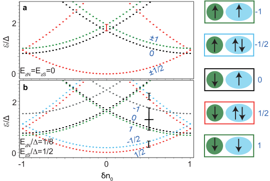
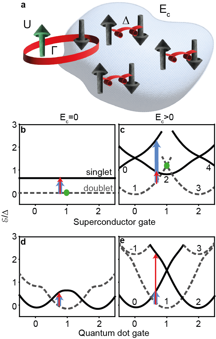
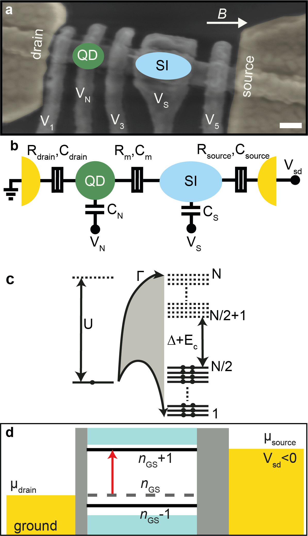
In a large superconductor, an adsorbed spin impurity binds to a quasiparticle screening cloud to form a state known as the Yu-Shiba-Rusinov (YSR) singlet, whose excitation energy with respect to the unbound doublet is below the superconducting energy gap, Yazdani et al. (1997). The miniaturization of the superconductor into an island reduces charge screening and introduces an energy gap for the addition of electrons, the Coulomb repulsion, (see Fig. 1a) Hergenrother et al. (1994); Higginbotham et al. (2015), with yet unexplored consequences on the ground state and the subgap spectrum. Such exploration is of relevance in the study of magnetic impurities adsorbed to superconducting droplets Vlaic et al. (2017); Yuan et al. (2020), in quantum-dot (QD) readout of Majorana qubits based on superconducting islands Albrecht et al. (2016); Plugge et al. (2017); Vaitiekėnas et al. (2020), and in realizations of superconducting variants of the multichannel Kondo model Potok et al. (2007); Žitko and Fabrizio (2017); Komijani (2020).
In the absence of a spin impurity, the charging of a superconducting island (SI) depends on the ratio , with leading to Cooper pair () charging and to charging Hergenrother et al. (1994); Higginbotham et al. (2015). In the latter case, even numbers of electrons condense as Cooper pairs, while a possible odd numbered extra electron must exist as an unpaired quasiparticle Higginbotham et al. (2015).
Here we provide the first spectral evidence of the many-body excitations in a superconducting Coulombic gap. The spin impurity resides in a gate-defined QD in an InAs nanowire, and the SI is an Al crystal grown on the nanowire with gate-tunable Coulomb repulsion. Both QD-SI and SI-QD-SI devices are investigated in this work. We demonstrate that a strong Coulomb repulsion forces exactly one quasiparticle in the SI to bind with the spin of the QD in the singlet ground state (GS). The Coulomb repulsion also enforces a positive-negative bias asymmetry in the position of the excitation peaks which is uncharacteristic of YSR excitations.
Results
Figures 1b-e summarize the energy dispersions which can arise when a QD is coupled to a superconductor. In Fig. 1b, the usual YSR case () with the QD gate-induced charge tuned to is depicted. The doublet GS and singlet excited state energies are independent of the gate-induced charge in the superconductor, , and excitations between these two states are electron-hole symmetric Jellinggaard et al. (2016). As shown in Fig. 1c, introducing in the superconductor produces a parabolic dispersion distorted by the hybridization () between the QD and the SI, which couples states of the same total charge. For odd , the energy of the doublet state is increased by (green dot), while for even it is the energy of the singlet state which is penalized by this amount. For odd and , the GS is a singlet even if . For , the singlet can be the GS if the YSR binding energy is large enough so that , which is achieved by increasing Pavešić et al. (2021).
Due to , the dispersion against is approximately parabolic in both the (up to a constant) and cases, as shown in Figs. 1d,e. For (Fig. 1d), the electron and hole excitations are symmetric due to the degeneracy of the even-parity parabolas. This ceases to be the case for (Fig. 1e). The asymmetry is maximal in the absence of additional QD levels. For (), an extra electron (hole) must be stored in the SI with excitation energy , but an extra hole (electron) can be added to either the QD or the SI, leading to a superposition of states with excitation energies and , where is the energy level of the QD (details on Extended Data Fig. 1). The extra electron or hole either forms a quasiparticle or a Cooper pair, depending on the parity of the SI occupation of the initial state. Superconducting Coulombic excitations (SCE) are only symmetric at the special gate points where the excited parabolas cross each other.

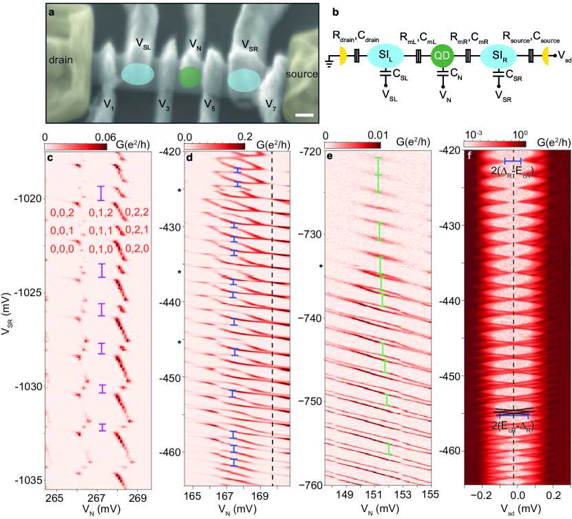
Our QD-SI device (Figs. 2a,b) is modelled as in the scheme shown in Fig. 2c Pavešić et al. (2021). The SI is conceived as several hundreds of electronic levels. Its charge is tuned by , equivalent to top gate voltage in the device. The corresponding Hamiltonian includes pairing between time-reversed states to produce the superconducting gap, , and coupling to the QD, , which is tuned by top gate voltage in the device. We consider constant Coulomb interactions for the QD, for the SI, and for the interdot charging due to the QD-SI inter-capacitance, (as in usual double QDs van der Wiel et al. (2002)). The QD is itself modelled as an Anderson impurity, whose charge is tuned by , equivalent to top gate voltage . Other top gates (, ) control the couplings of the QD and SI to the source and drain, not included in the model. The output of the model is the energy spectrum of the system, consisting of a few low-lying many-body states and the edge of the continuum. These states are sketched in Fig. 2d between the source and drain. Table 1 shows device and model parameters.
To record the spectrum of excitations between the low-lying many-body states, the device is biased by a source-drain bias voltage, , and the differential conductance, , is measured at the grounded drain, as shown in Fig. 2d. Asymmetric source and drain couplings are needed for to embody the energy asymmetry of the SCE. While we cannot account for the magnitude of , we expect that the measured reflects the excitation energies at , where the negative sign in the argument is necessary to account for the voltage drops and polarity conventions. Symmetric barriers would instead result in a trivial bias symmetry. A peak at one polarity thus demonstrates the existence, at the corresponding excitation energy, of an excited many-body state with electrons in the device, while a peak at the opposite polarity that of a many-body state with electrons, where is the total charge in the GS.
| (meV) | (meV) | (meV) | (meV) | (meV) |
|---|---|---|---|---|
| 0.05 | 0.8 -1.0 | 0.19 | 0.13 | |
| 0.04 | 0.8 | 0.18 | 0.2 | 0.16 |
The zero-bias signal exhibits a strong dependence on and , as shown in the diagram of Fig. 3a. Singletdoublet GS transitions are observed in the experiment when conductance lines are crossed, as at these lines appear when the and (or ) states in Fig. 2d are degenerate at zero energy. The repetition of the central hexagonal charge domain in the direction indicates filling of the SI. As a guide of the filling of the QD and the SI, we approximate their charge expectation values as integers , in each of the charge domains. This is an approximation as only is integer with Pavešić et al. (2021) (see Extended Data Fig. 1). Small but resolvable 1,1 singlet domains (an example is enclosed in a dotted line) are seen between the 1,2 and 1,0 doublet domains. In contrast, the lines to the sides of the central hexagonal domains, which separate the 0,0 and 0,2 domains and the 2,0 and 2,2 domains, show no splitting at this resolution. The difference stems from finite and , which stabilize the 1,1 but not the 0,1 and 2,1 domains. The presence of the 1,1 Coulomb-aided YSR singlet is the key difference from a trivial double QD stability diagram van der Wiel et al. (2002) and from the case Potok et al. (2007). For instance, a raise of the interdot coupling in a double QD introduces molecular orbitals which show as avoided crossings at triple points (TPs), whereas in the QD-SI system the YSR singlet is a many-body state for these parameters. Finite and are also responsible for increasing the distance between the points of multiple degeneracy, for the acute angle between vertical and horizontal conductance lines and, in the case of , for curving the conductance lines.
| 2.9 | 5 | 6.9 | 20 |
Our model of the system produces a diagram of GS transitions of the SCE that matches the gate position of the conductance lines, as shown in the comparison of the calculation to the experimental data in Fig. 3a. The quality of the match for model parameters approximately similar to the experimentally measured values (with as the only fit parameter) constitutes a first proof of the presence of SCE in our device.
We corroborate the spin () assignment done in Fig. 3a (right panel) at from the variation of GS domain sizes with T (in inset). Doublet domains are stabilized by more than singlet domains, while triplet domains are stabilized further than doublet and singlet domains. The model fits the data using the -factors as free parameters, and taking into account the GS transition from singlet to triplet in the 1,1 charge sector (charge parabolas are shown in Extended Data Fig. 2). The -factors in the Hamiltonian are significantly larger than the measured effective -factors (see Table 2). These bare factors produce Zeeman splittings and in the QD and the SI, where is the Bohr magneton. The effective and bare factors would be equal if the expectation values of the QD and the SI charges increased in steps of exactly across the GS transition lines. For non-zero , (non-integer) charge distributions occur between the QD and the SI on either side of the GS transition line (see Extended Data Fig. 1), hence the effective -factors are some non-trivial function of the true (bare) -factors which appear in the Hamiltonian van Gerven Oei et al. (2017).
Following this comprehensive mapping, we show in Fig. 3b the spectrum at finite versus for fixed , at which the SI contains only Cooper pairs in the GS up to a good approximation. The SCE have a double-S shape, spanning mV. They are approximately inversion symmetric in position and in intensity with respect to the electron-hole gate-symmetric filling point of the QD, which corresponds to the center of the 1,0 sector (indicated by a cross), from where removing/adding an electron from/to the QD are equally energetically unfavorable. jumps in intensity when the SCE cross zero bias, as highlighted by the insert traces at gate points before (grey) and after (black) one of such changes. While the SCE are expected to appear as a pair at asymmetric positive and negative bias positions for a given gate voltage, in practice only one SCE is observed. A GS change brings discontinuously up to the continuum the other state, as charge is suddenly redistributed between the QD and the SI Pavešić et al. (2021).
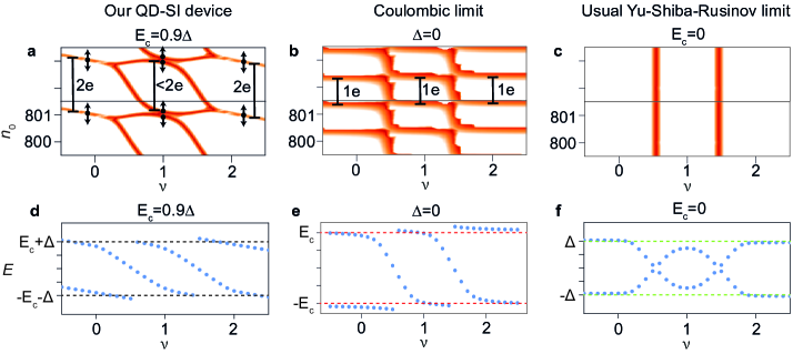
Our model reproduces the position of the subgap resonances, as evidenced in the overlay of the calculated spectrum on the experimental data in Fig. 3b (see also Extended Data Fig. 3). Differences between the SCE spectrum and the spectrum in the Coulombic () and Yu-Shiba-Rusinov () limits are shown in Extended Data Fig. 4. The Coulombic spectrum bears resemblance to that of an impurity in the paramagnetic Mott insulator described by the Hubbard model Imada et al. (1998); Sachdev (2003), despite the differences in the Hamiltonian (local Hubbard interaction versus constant Coulomb repulsion in our model). In both cases the charge transfer from the impurity site to the bath costs energy corresponding to the total charge gap of the system in the absence of the impurity ( in the Hubbard model at half-filling, in our device), and in both cases there is a (quasi)continuum of fermionic states extending above this gap (doublons/holons in a Mott insulator, and Coulomb quasiparticles with a mixed character of Bogoliubov quasiparticles due to in our device), leading to the same phenomenology.
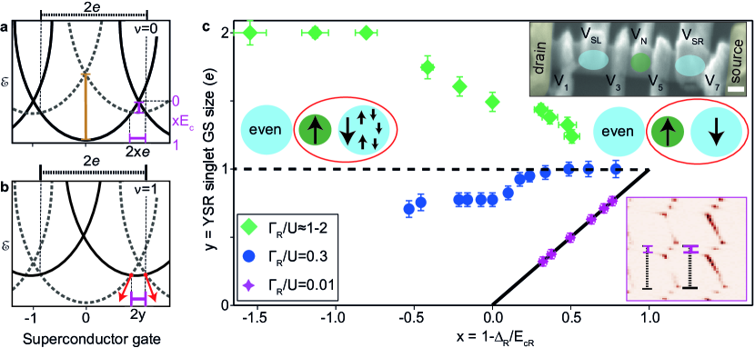
To map these limits, we vary continuously the Coulomb repulsion in the superconductor in a second device. We first explore the role of the Coulomb repulsion on the stability of the YSR singlet as the GS. To this aim, we define two quantities, , and , the YSR singlet GS size in units of . In the regime, . Figs. 4a,b explain how and are experimentally extracted. In the limits when and , and , respectively. When , then . Fig. 4c shows a measurement of versus in a device consisting of a QD coupled to two SIs with hybridization and (top inset in Fig. 4c). The SIs have charging energies and and superconducting gaps and , and their occupations are tuned with top gate voltages and . The advantage of this three-component device over the two-component one is that the presence of only one QD between the two SIs can be verified from stability diagrams similar to that in Fig. 3a against the pairs of gate voltages (,) and (,). In Fig. 4c, characterizes the GS stability of the YSR state formed by the binding of the QD spin to the quasiparticle cloud in the right SI, and . To employ the device as this two-component system, the left SI is kept either as a cotunnnelling probe at even occupation (for ) or as a soft-gap superconducting probe (for and ). Three QD shells with different values of are analyzed. At the weakest , shows a trivial linear dependence with a slope of 1 and with endpoints at (0,0) and (1,1), connected by a fitted solid line in the graph. In this regime, only stabilizes the YSR singlet as the GS. At the other extreme, at the largest , stabilizes the doublet more strongly than the YSR singlet, reducing . In between these two extremes, at , the behavior is intermediate. When , converges to independently of , as stabilizes equally well the doublet and singlet states for even and odd gate-induced charges in the right SI. In the other limit, when , depends exclusively on , as in the usual YSR regime.
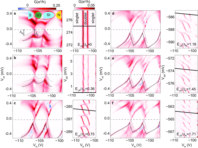
Next, we describe how the Coulomb repulsion in the superconductor affects the dispersion of the excitations and how this is related to changes in the stability diagram. In Fig. 5, we show the evolution of the excitations produced by one QD shell on the right SI over a wide range of , corresponding to a charge variation of electrons. In this range, goes from 0 to 1.71, as measured from Coulomb-diamonds spectroscopy. The increase in is reflected on the stability diagram. In the usual YSR regime (Fig. 5a), the diagram shows two vertical dispersionless lines, and the spectrum consistently displays a YSR loop (for measurement details, see Methods). When the right SI enters into Coulomb blockade (Fig. 5b, ), the lines in the stability diagram wiggle as interdot charging and tunnelling effects enter into consideration. Consequently, the YSR loop in the spectrum gets skewed rightwards and increases its bias size as the energy gap includes now a Coulombic component. At (Fig. 5c), the entrance of the 1,1 YSR singlet GS breaks the stability diagram into several domains, and the excitations adopt a double-S shape. At this setting, the 1,0 doublet domain has a size , where is the YSR binding energy of the spin in the QD to the quasiparticle cloud in the right SI. This results in a maximum of the bias size of the double-S shape excitation. From then on, an increase in in Figs. 5d-f reduces the energy of the doubletsinglet excitation and the double-S shaped feature shrinks in bias size, concomitantly with the stronger stabilization of the YSR 1,1 singlet GS in the stability diagram.
Throughout this article, we provided compelling evidence for the existence of superconducting Coulombic subgap excitations arising from states bound to a semiconductor-superconductor interface, and we showed how these are related to the usual electron-hole symmetric Yu-Shiba-Rusinov excitations. On one hand, we showed that a small Coulomb repulsion in the superconductor is enough to turn the excitations asymmetric in the polarity of the bias voltage. On the other hand, a strong Coulomb repulsion () converts the YSR singlet many-body state into a two-body state formed by a spin in the QD and a single quasiparticle in the superconductor.
Though our model is successful at matching excitation energies, an extension which includes transport is needed to account for the magnitude of the conductance features and for their bias positions in devices with more symmetric source-drain barriers. The observation of current blockade in a regime of weaker hints at elastic cotunnelling as the transport mechanism in our QD-SI device (see Section II of Supplementary Information). The absence of zero-bias in the regime (e.g. Extended Data Fig. 5) indicates that Andreev reflection ( charge transfer) is not a transport mechanism in our devices in this regime. Due to charge transfer between the SI and the QD, the model indicates that an upwards reconsideration of bare -factor values extracted from experimentally-determined -factors of subgap excitations is needed to match the experimental results Shen et al. (2018); Albrecht et al. (2016). Based on its success, the model can also inform on future developments, e.g. qubit and multi-channel devices which utilize the SI-QD-SI device, as outlined in Ref. Pavešić and Žitko (2021).
The system sketched in Fig. 1a may also be realized with magnetic adatoms on superconducting droplets (e.g. Pb on an InAs substrate), and probed with scanning tunnelling microscopy Vlaic et al. (2017); Yuan et al. (2020). Several open questions could be answered with this technique: What is the spatial extension of the excitations in a superconducting Coulombic energy gap Ménard et al. (2015)? Is there orbital structure in the excitations Ruby et al. (2016)? How do the excitations behave in chains of magnetic adatoms when these chains are deposited on top of a SI Schneider et al. (2021)? Do chains of magnetic adatoms deposited on finite SIs support Majorana excitations Nadj-Perge et al. (2014)?
Methods
Devices fabrication and layout. QD-SI device (Fig. 2a). A 110-nm wide InAs nanowire picked with a micromanipulator was contacted by 5/200 nm Ti/Au (in yellow) source and drain leads. The 350-nm long, 7-nm thick epitaxially-grown Al SI covering three facets of the nanowire was defined by chemically etching the upper and lower sections of the nanowire before contacting. After insulating the nanowire and the leads with a 6-nm thick film of HfO2, five Ti/Au top gates were deposited along the nanowire. The QD was defined in the bare nanowire next to the SI by setting top gates 1 and 3 to negative voltage. A Si/ substrate backgate was kept at zero voltage throughout the experiment.
SI-QD-SI device (Extended Data Fig. 5). The SI-QD-SI device was fabricated using a nanowire from the same growth batch. Two nominally identical 7-nm thick, 300-nm long, epitaxially-grown Al SIs were defined by chemical etching. The nanowire was contacted by 5/200 nm Ti/Au leads, and then insulated by a 5-nm thick layer of from seven Ti/Au top gates deposited after. The QD was defined between the two SIs by setting top gates 3 and 5 to negative values. The substrate backgate was used to aid the top gates in depleting the device. was tuned by using an auxiliary QD (QD) defined between the right SI and the source lead. When QD was put near resonance by sweeping , could be tuned to negative values, and when QD was put in cotunnelling, could be tuned to positive values. Similarly, was tuned using an auxiliary QD defined between the left SI and the drain lead.
The critical of the superconducting Al film was measured to be T in nanowire devices made from the same batch of nanowires used in the fabrication of the present device Estrada Saldaña et al. (2018, 2020), which left ample room for -resolved measurements in the superconducting state. In the QD-SI and SI-QD-SI devices, the presence of superconductivity at large was determined from size differences of adjacent charge domains with odd and even occupation of the SI, observed up to T and T, respectively. Larger was not explored.
Differential conductance measurements. A standard lock-in technique was used to measure the differential conductance, , of the QD-SI device by biasing the source with an AC excitation of 5 V at a frequency of 223 Hz on top of a DC source-drain bias voltage, , and recording the resulting AC and DC currents on the grounded drain lead. In the case of the SI-QD-SI device, was measured at the grounded drain with a 5 V lock-in excitation applied at the source at 84.29 Hz. The measurements were performed in an Oxford Triton dilution refrigerator at 30 mK for the QD-SI device and 35 mK for the SI-QD-SI device, such that , where is the Boltzmann constant and is the refrigerator temperature.
Calculation of subgap and continuum excitations. The calculations were done using the density-matrix renormalization group approach (details in Section III of Supplementary Information). The quantum numbers are the total number of electrons in the system, , the z-component of the total spin, (see Extended Data Fig. 2), and the index for states in a given (, ) sector, . The superconducting Coulombic excitation energies are given by . The edges of the continuum excitations are given by . Due to the finite size of the SI, the continuum is in truth only a quasi-continuum of states. The nature of these states and the excitation energies depend on the values of and . For , the quasiparticles are free-electron states. For , these are Bogoliubov quasiparticles with pronounced inter-level pairing correlations . If , the excitation spectrum is not affected by the number of preexisting particles in the superconductor (up to finite-size effects). If , the particle-addition and particle-removal energies are affected by the charge repulsion (parabolas). The calculations do not provide direct results for the differential conductance of the system, only information about the energies of the GS and the low-lying excitations.
Spectral measurements in Fig. 5. To obtain sharp spectral features visible over the continuum background, we tuned the left SI into a superconducting probe (, ). The strong hybridization of the left SI with the drain needed to achieve resulted in an unintended soft gap in this probe, which produced faint replica of the main excitations. For example, in Fig. 5a, black dotted lines correspond to the YSR loop coming from the QD-right SI being probed by the coherence peaks of the probe. The loop is thus followed by negative differential conductance (NDC) and appears at , reaching at GS transitions. The gray dotted lines highlight a YSR replica probed by the soft gap of the probe, thus an order of magnitude weaker in conductance and without associated NDC. This replica appears at , and therefore crosses zero bias at GS transitions. When increases, the relationships between the excitations and the bias positions of the conductance features become approximations due to non-ideal , asymmetry in the device, which also results in negative-slope features included in the dotted lines but not accounted by the model, as the model does not consider transport. The interpretation of features in the continuum at higher bias is outside the scope of this work.
Data availability
Raw experimental data shown in the paper is available at the data repository ERDA of the University of Copenhagen in this link.
References
- Yazdani et al. (1997) Ali Yazdani, B. A. Jones, C. P. Lutz, M. F. Crommie, and D. M. Eigler, “Probing the Local Effects of Magnetic Impurities on Superconductivity,” Science 275, 1767–1770 (1997).
- Hergenrother et al. (1994) J. M. Hergenrother, M. T. Tuominen, and M. Tinkham, “Charge transport by Andreev reflection through a mesoscopic superconducting island,” Phys. Rev. Lett. 72, 1742–1745 (1994).
- Higginbotham et al. (2015) A. P. Higginbotham, S. M. Albrecht, G. Kiršanskas, W. Chang, F. Kuemmeth, P. Krogstrup, T. S. Jespersen, J. Nygård, K. Flensberg, and C. M. Marcus, “Parity lifetime of bound states in a proximitized semiconductor nanowire,” Nat. Phys. 11, 1017–1021 (2015).
- Vlaic et al. (2017) Sergio Vlaic, Stéphane Pons, Tianzhen Zhang, Alexandre Assouline, Alexandre Zimmers, Christophe David, Guillemin Rodary, Jean-Christophe Girard, Dimitri Roditchev, and Hervé Aubin, “Superconducting parity effect across the Anderson limit,” Nat. Commun. 8, 1–8 (2017).
- Yuan et al. (2020) Yonghao Yuan, Xintong Wang, Canli Song, Lili Wang, Ke He, Xucun Ma, Hong Yao, Wei Li, and Qi-Kun Xue, “Observation of Coulomb Gap and Enhanced Superconducting Gap in Nano-Sized Pb Islands Grown on SrTiO3,” Chin. Phys. Lett. 37, 017402 (2020).
- Albrecht et al. (2016) S. M. Albrecht, A. P. Higginbotham, M. Madsen, F. Kuemmeth, T. S. Jespersen, J. Nygård, P. Krogstrup, and C. M. Marcus, “Exponential protection of zero modes in Majorana islands,” Nature 531, 206–209 (2016).
- Plugge et al. (2017) Stephan Plugge, Asbjørn Rasmussen, Reinhold Egger, and Karsten Flensberg, “Majorana box qubits,” New J. Phys. 19, 012001 (2017).
- Vaitiekėnas et al. (2020) S. Vaitiekėnas, G. W. Winkler, B. van Heck, T. Karzig, M.-T. Deng, K. Flensberg, L. I. Glazman, C. Nayak, P. Krogstrup, R. M. Lutchyn, and C. M. Marcus, “Flux-induced topological superconductivity in full-shell nanowires,” Science 367, eaav3392 (2020).
- Potok et al. (2007) R. M. Potok, I. G. Rau, Hadas Shtrikman, Yuval Oreg, and D. Goldhaber-Gordon, “Observation of the two-channel Kondo effect,” Nature 446, 167–171 (2007).
- Žitko and Fabrizio (2017) Rok Žitko and Michele Fabrizio, “Non-Fermi-liquid behavior in quantum impurity models with superconducting channels,” Phys. Rev. B 95, 085121 (2017).
- Komijani (2020) Yashar Komijani, “Isolating Kondo anyons for topological quantum computation,” Phys. Rev. B 101, 235131 (2020).
- Jellinggaard et al. (2016) Anders Jellinggaard, Kasper Grove-Rasmussen, Morten Hannibal Madsen, and Jesper Nygård, “Tuning Yu-Shiba-Rusinov states in a quantum dot,” Phys. Rev. B 94, 064520 (2016).
- Pavešić et al. (2021) Luka Pavešić, Daniel Bauernfeind, and Rok Žitko, “Subgap states in superconducting islands,” Phys. Rev. B 104, L241409 (2021).
- van der Wiel et al. (2002) W. G. van der Wiel, S. De Franceschi, J. M. Elzerman, T. Fujisawa, S. Tarucha, and L. P. Kouwenhoven, “Electron transport through double quantum dots,” Rev. Mod. Phys. 75, 1–22 (2002).
- van Gerven Oei et al. (2017) W.-V. van Gerven Oei, D. Tanasković, and R. Žitko, “Magnetic impurities in spin-split superconductors,” Phys. Rev. B 95, 085115 (2017).
- Imada et al. (1998) Masatoshi Imada, Atsushi Fujimori, and Yoshinori Tokura, “Metal-insulator transitions,” Rev. Mod. Phys. 70, 1039–1263 (1998).
- Sachdev (2003) Subir Sachdev, “Colloquium: Order and quantum phase transitions in the cuprate superconductors,” Rev. Mod. Phys. 75, 913–932 (2003).
- Shen et al. (2018) Jie Shen, Sebastian Heedt, Francesco Borsoi, Bernard van Heck, Sasa Gazibegovic, Roy L. M. Op het Veld, Diana Car, John A. Logan, Mihir Pendharkar, Senja J. J. Ramakers, Guanzhong Wang, Di Xu, Daniël Bouman, Attila Geresdi, Chris J. Palmstrøm, Erik P. A. M. Bakkers, and Leo P. Kouwenhoven, “Parity transitions in the superconducting ground state of hybrid InSb–Al Coulomb islands,” Nat. Commun. 9, 1–8 (2018).
- Pavešić and Žitko (2021) Luka Pavešić and Rok Žitko, “Qubit based on spin-singlet Yu-Shiba-Rusinov states,” arXiv (2021), 2110.13881 .
- Ménard et al. (2015) Gerbold C. Ménard, Sébastien Guissart, Christophe Brun, Stéphane Pons, Vasily S. Stolyarov, François Debontridder, Matthieu V. Leclerc, Etienne Janod, Laurent Cario, Dimitri Roditchev, Pascal Simon, and Tristan Cren, “Coherent long-range magnetic bound states in a superconductor,” Nat. Phys. 11, 1013–1016 (2015).
- Ruby et al. (2016) Michael Ruby, Yang Peng, Felix von Oppen, Benjamin W. Heinrich, and Katharina J. Franke, “Orbital Picture of Yu-Shiba-Rusinov Multiplets,” Phys. Rev. Lett. 117, 186801 (2016).
- Schneider et al. (2021) Lucas Schneider, Philip Beck, Thore Posske, Daniel Crawford, Eric Mascot, Stephan Rachel, Roland Wiesendanger, and Jens Wiebe, “Topological Shiba bands in artificial spin chains on superconductors,” Nat. Phys. 17, 943–948 (2021).
- Nadj-Perge et al. (2014) Stevan Nadj-Perge, Ilya K. Drozdov, Jian Li, Hua Chen, Sangjun Jeon, Jungpil Seo, Allan H. MacDonald, B. Andrei Bernevig, and Ali Yazdani, “Observation of Majorana fermions in ferromagnetic atomic chains on a superconductor,” Science 346, 602–607 (2014).
- Estrada Saldaña et al. (2018) J. C. Estrada Saldaña, A. Vekris, G. Steffensen, R. Žitko, P. Krogstrup, J. Paaske, K. Grove-Rasmussen, and J. Nygård, “Supercurrent in a Double Quantum Dot,” Phys. Rev. Lett. 121, 257701 (2018).
- Estrada Saldaña et al. (2020) Juan Carlos Estrada Saldaña, Alexandros Vekris, Victoria Sosnovtseva, Thomas Kanne, Peter Krogstrup, Kasper Grove-Rasmussen, and Jesper Nygård, “Temperature induced shifts of Yu–Shiba–Rusinov resonances in nanowire-based hybrid quantum dots,” Commun. Phys. 3, 1–11 (2020).
Acknowledgements
We thank Jens Paaske and Silvano De Franceschi for useful discussions.
Funding: The project received funding from the European Union’s Horizon 2020 research and innovation program under the Marie Sklodowska-Curie grant agreement No. 832645, the FET Open AndQC and the Novo Nordisk Foundation project SolidQ. We additionally acknowledge financial support from the Carlsberg Foundation, the Independent Research Fund Denmark, QuantERA ’SuperTop’ (NN 127900), the Danish National Research Foundation, Villum Foundation project No. 25310, and the Sino-Danish Center. P. K. acknowledges support from Microsoft and the ERC starting Grant No. 716655 under the Horizon 2020 program. L. P. and R. Ž. acknowledge the support from the Slovenian Research Agency (ARRS) under Grant No. P1-0044 and J1-3008.
Author contributions
J.C.E.S. and A.V. performed the experiments. P.K. and J.N. developed the nanowires. J.C.E.S., A.V., K.G.-R., J.N., L.P. and R.Ž. interpreted the experimental data. L.P. and R.Ž. did the theoretical analysis. J.C.E.S. wrote the manuscript with input from A.V., K.G.-R., J.N., L.P. and R.Ž.
Competing interests
The authors declare no competing interests.