Effects of spin orbit coupling in superconducting proximity devices – application to \ceCoSi2/\ceTiSi2 heterostructures
Abstract
Motivated by the recent findings of unconventional superconductivity in \ceCoSi2/\ceTiSi2 heterostructures, we study the effect of interface induced Rashba spin orbit coupling on the conductance of a three terminal “T” shape superconducting device. We calculate the differential conductance for this device within the quasi-classical formalism that includes the mixing of triplet-singlet pairing due to the Rashba spin orbit coupling. We discuss our result in the light of the conductance spectra reported by Chiu et al.for \ceCoSi2/\ceTiSi2 heterostructures.
Introduction– The search for platforms that can host Majorana zero modes (MZMs) has been one of the major topics driving current condensed matter research as MZMs, being localized quasiparticles that obey non-Abelian braiding statistics, are the essential ingredient for topological quantum computingRead and Green (2000); Kitaev (2001); Ivanov (2001); Kitaev (2003); Wilczek (2009); Nayak et al. (2008). Early proposals for creating MZMs involve spin triplet superconductivity while almost all known superconductors belong to the spin singlet class with a few possible exceptions such as \ceUPt3. As a result, a variety of ingenious heterostructures of superconducting nano-wires have been proposed and observed to generate the required wave pairing component, taking advantage of broken time-reversal and inversion symmetryLutchyn et al. (2010); Oreg et al. (2010); Mourik et al. (2012); Nadj-Perge et al. (2014). MZM has also been proposed inside a vortex of topological superconductor Volovik (2003); the experimental observation of MZM in some of the iron-based superconductors is along this lineWang et al. (2018); Liu et al. (2018). Fu and Kane Fu and Kane (2008) proposed that proximity of s-wave superconductor on surface of 3D topological insulator may serve for the same purpose to generate MZMs, due to the spin-momentum locking. Their proposal has been confirmed experimentallySun et al. (2016).
To distinguish between singlet and triplet superconductors, in addition to nuclear magnetic resonanceMackenzie and Maeno (2003) and -spin rotation probe, a T-shaped proximity structure junction was proposed to probe into the presence of triplet superconductivity Asano et al. (2007). The proposed device consists of two normal metal wires combined to form the letter ‘T’. This three-terminal device is connected to a superconductor at the free end of the leg, see Fig. 1. As shown in Ref. Asano et al. (2007), a chiral wave or an ordinary wave state give a zero bias conductance peak (ZBCP) in response to a bias voltage between the open ends of the bar of the ‘T’.
Recent experimental results reported by Chiu et al. have been argued to be consistent with the occurrence of chiral wave pairing in \ceCoSi2/\ceTiSi2 heterostructures Chiu et al. (2020). Chiu et al. support their claim with conductance spectroscopy data of \ceCoSi2/\ceTiSi2 superconductor-normal metal (SN) tunnel junctions. In these heterostructures, \ceCoSi2 is the superconducting component which becomes superconducting below K. The conductivity of the SN tunnel junctions agrees with the theoretical calculations based on the Blonder-Tinkham-Klapwijk (BTK) model for a chiral wave superconductorBlonder et al. (1982). However, there is a sharp zero bias peak in the conductance spectra of the SN junction, which cannot be described within the BTK theory.
Chiu et al. further substantiate their interpretation with conductance spectra based on three terminal T-shaped proximity devices similar to the one sketched in Fig. 1, which again show ZBCPs. As noted in Ref. Chiu et al. (2020), a distinction between ordinary and chiral wave superconductor solely based on experimental conductance spectra is hardly feasible. The observation of hysteresis behavior in the magnetoresistance below superconducting transition temperature of the \ceCoSi2/\ceTiSi2 junctions, however, further vindicates their claim of chiral wave in the \ceCoSi2/\ceTiSi2 heterostructures. The findings of Ref. Chiu et al., 2020 are intriguing for a few reasons. The superconductivity in \ceCoSi2 was discovered in 1952Matthias (1952), the theoretical estimate of based on phonon mediated pairing appears to agree well with the experimental Mattheiss and Hamann (1988). The specific heat data below superconducting state suggests conventional wave pairingTsutsumi et al. (1997). This material does not appear to be located in the vicinity of magnetism, therefore there is no reason to expect it to be a chiral wave superconductor, at least in the bulk limit.
It is worth noting that a strong spin-orbit coupling (SOC), exceeding the superconducting gap of \ceCoSi2 by more than a factor 30, has been reported in \ceCoSi2 by the same groupChiu et al. (2020). Having in mind this strong SOC, we propose the substrate induced Rashba SOC as a source of wave pairing in this system. It is known that SOC induced pairing does not break the time reversal symmetryGor’kov and Rashba (2001), and the presence of the SOC also leads to mixing of the triplet and the singlet components. In the context of noncentrosymmetric superconductors, the tunneling conductance for SN junctions has been studied in systems with SOCIniotakis et al. (2007); Vorontsov et al. (2008); Tanaka et al. (2010); Eschrig et al. (2012); Tamura and Tanaka (2019). However, the effect of the SOC and the conductance for a mixed parity superconductor in a T-junction device is not known. The original T-junction study did not include the SOC, and the ZBCP for a chiral wave superconductor is expected to be weakAsano et al. (2007).
In this paper, we investigate the effect of the singlet-triplet mixing on the conductance spectra of the T-shaped junctions. In the context of \ceCoSi2/\ceTiSi2 heterostructures, we focus on substrate induced SOC in a superconductor, which results in the “” pairing state, where the singlet component has wave symmetry and the triplet component has wave symmetry. In principle, triplet and singlet components can have anisotropic structures due to the orbital form factors and because the bands crossing the Fermi energy derive from the 3d orbitals of \ceCo Mattheiss and Hamann (1988). Thus, we also consider the “” and “” pairing states, which have additional orbital form factors compatible with and functions, which lead to and structures for the singlet components and effectively -wave and -wave like structures for the triplet components, respectively. The state has been proposed for a few heavy electron noncentrosymmetric systemsTada et al. (2008); Yanase and Sigrist (2008) and the state has been suggested for \ceLaAlO3/\ceSrTiO3 heterointerfacesTanaka et al. (2010).
Model & Formalism– We model the \ceCoSi2/\ceTiSi2 T-shaped junction of Ref.Chiu et al. (2020) in terms of the two-dimensional proximity devices depicted schematically in Fig. 1. The transport in the normal metal (NM) part is assumed to be diffusive which is the experimentally relevant regime.
The height () and the width () are very small compared to its length () in either direction and its dimensions are assumed to be very small compared to the coherence length (i.e., ), where and are the Fermi velocity and the superconductivity gap, respectively. Within the ambit of these assumptions, this structure can be thought of a set of two one dimensional wires joined to form the shape of the letter ‘T’. The leg of this T-shaped junction is attached to a clean superconductor. The ends of the horizontal section of this junction are subjected to a bias voltage (). We consider the case where the SOC exists in the superconducting component of this structure due to its broken inversion symmetry.
The kinetic part of the Hamiltonian reads,
| (1) |
Here is the electronic dispersion relation for the fermions and the SOC term is,
| (2) |
where is the Rashba SOC coupling constant, is the effective mass and is (), where are the Pauli matrices in spin space. We consider the Rashba SOC, that is induced along the growth direction, which is chosen to be the direction in the T-shaped junction. In this case, the normal to the relevant interface is along the axis and the SOC vector is,
| (3) |
where is the angle in the two dimensional momentum space.
Diagonalizing the Hamiltonian results in a splitting of the original band into two helical bands with different spin structures. The energies of these two bands are . The difference in the density of states and the Fermi velocities are of the order of , where and are the Fermi momentum and the Fermi energy of the original band. For realistic systems, the SOC energy is generally very small compared to the Fermi energy. Therefore, we ignore this difference in the density of states and the Fermi velocities between the helical bands and we take these parameters to be the same as the original band for our subsequent calculations.
We assume that the superconducting component is confined in the two-dimensional plane and that it has dimensions that are very large compared to the coherence length, hence we treat it like a homogeneous system, and ignore any kind of inverse proximity effect due to the junction formation. We adopt the quasi-classical Keldysh formalism to carry out the conductance calculationsUsadel (1970), where the quasi-classical Green’s function consists of retarded, advanced and Keldysh components. Each of these components is a matrix in the Nambu-spin space. We denote the Green’s function in this space with and denotes the Green’s functions in the spin basis. The advanced and Keldysh components can be obtained from the retarded component, on which we focus in the following. Following Ref. Hayashi et al., 2006, the quasi-classical retarded Green’s function in a superconductor without inversion symmetry can be expressed as,
| (4) |
where , , , and . The general gap structure for a system with the SOC isFrigeri et al. (2004); *FrigeriArxiv,
| (5) |
Here the SOC vector acts like the vector, and () is the gap magnitude of the singlet (triplet) component. The gaps on two helical bands are . The angular anisotropy of the gaps are embedded in and . The simplest case is , which is referred as state, where the singlet component is an isotropic wave state, and the triplet component has wave structure. Such states have been proposed for various non-centrosymmetric superconductors. Apart from this, the other possibilities are the state, where , and the state with . We focus on state, which is more relevant in the context of \ceCoSi2/\ceTiSi2 heterostructures. The gap function is parameterized as
| (6) |
where is Annunziata et al. (2012). Here the parameter is the ratio of triplet to singlet component.
The Cooper pairs from the superconducting side can tunnel into the diffusive normal metal (NM), and this effect is included through the boundary conditions, which are used to solve the Usadel equations on the NM side. We treat the barrier between the NM and the superconductor as a spin-independent barrier. This assumption is justified because the SOC is very small compared to the Fermi energyEschrig et al. (2012). We first calculate the retarded component of the quasi-classical Green’s function , and then construct the advanced and the Keldysh components using . The subscript denotes the normal metal. The Usadel equations for are
| (7) |
where is the diffusion constant of the normal metal, denotes the spatial directions , and is . The normalization condition for the quasi-classical Green’s function is,
| (8) |
These equations are supplemented by the boundary conditions,
| (9) | |||||
| (10) |
where the last condition reflects current conservationZaitsev (1994). The boundary condition at depends on the nature of the gap in the superconductor. We use the boundary condition derived by Nazarov for interfaces with arbitrary transparencyNazarov (1999), which was generalized for unconventional superconductors by Tanaka et alTanaka et al. (2003, 2004a); *Tanaka2004_ERR; Tanaka et al. (2005a); *Tanaka2005_ERR. In this approach, the interface is modeled as a function potential barrier , which has the transmission probability,
| (11) |
where is the angle measured with respect to the normal to the interface, which is axis in the geometry we consider, and is a dimensionless parameter given by . Here is the effective mass and is the Fermi momentum. A large value of gives an interface with poor transparency, whereas characterizes a transparent interface. The boundary condition at the SN interface can be expressed as,
| (12) |
where at the right hand side of Eq. (12) is the quasi-classical Green’s function in the NM region evaluated at , and is the ratio of the normal metal resistance , and the interface resistance . The angular average at the right hand side of Eq.(12) is defined as,
| (13) |
Note, the angle in the boundary condition is measured with respect to the interface normal. The matrix function in Eq. (12) is,
| (14) | |||||
| (15) | |||||
| (16) |
Note, the boundary condition itself depends on the solution at the boundary. To calculate the differential conductance, we first calculate the current. For the current calculation, we need the Keldysh component of the quasi-classical Green’s function,
| (17) |
where the advanced component is,
| (18) |
and the spin resolved distribution function is a diagonal matrix Morten et al. (2005), where and are the transverse and the longitudinal distribution functions and is the spin index. In the T-shaped junction, a bias voltage () is applied at and at the other end the voltage is kept at zero. Therefore, the equilibrium spin-resolved distribution functions at these two ends are,
| (19) | |||||
| (20) |
Here is the Fermi-Dirac distribution function and . The transverse component of the distribution function will be the same for both spin components at the normal electrode. The charge current density is,
| (21) |
Here is the total density of states at the Fermi level. The differential conductance can be obtained by evaluating the derivative of the charge current density w.r.t. the bias voltage – we numerically solve the Usadel equations in the normal metal and with the aforementioned boundary conditions. Since the boundary condition at the SN interface involves the solutions at the interface, so we start with a guess solution and obtain the final solution self-consistently.
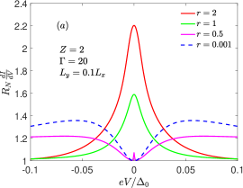
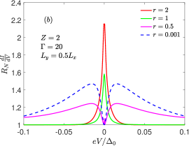
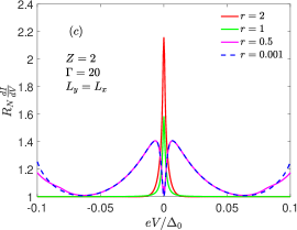
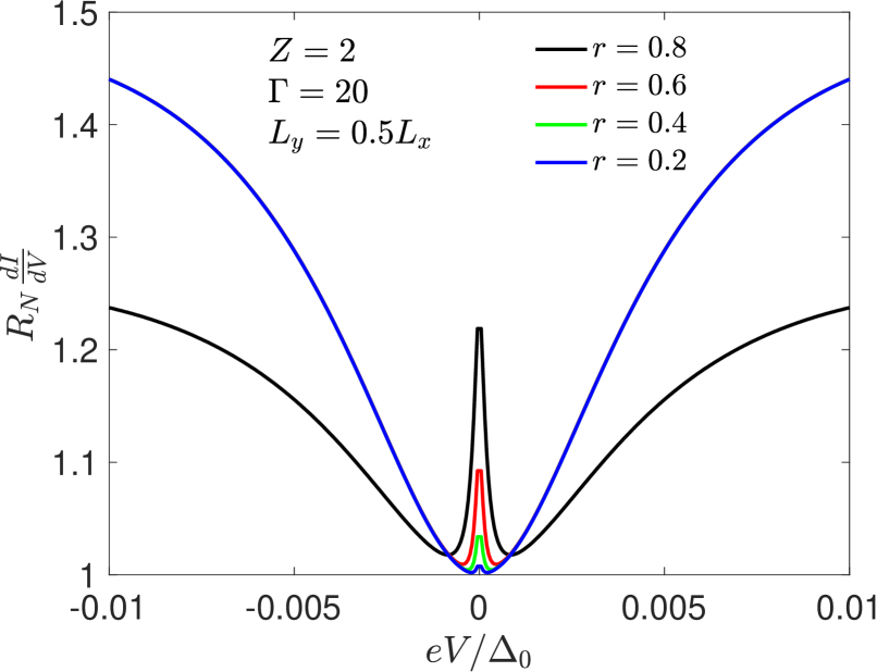
Results & Discussion– We consider a good interface between NM and SC and fix at a value of . The interface barrier parameter is set to . A larger value of represents a good quality surface, which is essential for the formation of a sizable proximity effect. Figure 2 shows the differential conductance for the T-shaped device, where the superconducting portion is under the influence of the substrate induced Rashba SOC for several values of the parameter indicating the relative strength of the triplet component. The magnitude of the gap is , where is the Thouless energy for the half wire along the direction i.e. . For the proximity problem, the characteristic energy scale in the NM is the Thouless energy, which is inversely proportional to the square of the device length. A smaller devices is usually better for observing proximity effect related physics.
For large values of , the triplet component dominates. In this regime we find that the differential conductance is similar to the -wave caseAsano et al. (2007). In general, for a three dimensional system, a Rashba SOC gives , where is the polar angle. Therefore, a triplet dominated system will have horizontal line nodes. However, in our study we consider a two-dimensional system, where the gaps on the two helical bands are . Thus, in the triplet dominant limit (), we have isotropic unequal gaps on two bands with opposite chiralities. A zero bias conductance peak (ZBCP) is expected for a chiral -wave superconductorAsano et al. (2007), however it is expected to be weaker than a wave system. We find that the height of the peak is comparable to that of a wave system. Unlike in a chiral wave superconductors, the time-reversal symmetry is not broken in the case considered here. The origin of the peak is the symmetry of the induced pairing in NM. In the diffusive metal, the isotropic wave state can survive due to impurity scattering, which kills any other kind of superconducting state. In the superconducting side of the junction, both triplet and singlet components are even functions of frequency. Therefore, the triplet component leaks odd frequency, even parity and spin triplet pairs, and the odd frequency nature of these induced pair gives rise to a ZBCPTanaka et al. (2005b); *TanakaTriplet_ERR; Tanaka and Golubov (2007). In the case of two helical bands with opposite chirality triplet state, the spectral weight of the ZBCP is larger than that expected for a chiral superconductor. The ZBCP becomes sharper as the length of the leg () attached to the superconductor increases, therefore a T-shaped junction with a shorter leg provides a better chance of ZBCP detection. We find that a ZBCP forms as long as the triplet component is stronger. For the special case of , when triplet and singlet components are equal, we still find a ZBCP in the differential conductance albeit with a reduced height and width. Since one of the bands has a zero gap in this limit, the height of the peak decreases – the origin of the reduced width in the ZBCP for smaller is the presence of even frequency, spin singlet and even parity pairs, which comes from the singlet component in the mixed parity superconducting state. Such pairs reduce the density of states at the Fermi level, which reduces the conductivity. However, induced pairs also increase conductivity in the diffusive metal, this increase comes through Maki-Thompson like processVolkov and Takayanagi (1996); *VolkovTakayanagi2. These two counter effects cancel at zero energy. The finite energy maximum in the conductivity near the Thouless energy scale arises due to different decay patterns of these two effects. The negative contribution from the loss of density of states decays exponentially, while the Maki-Thompson like contribution decays non-exponentially over the energy scale of . These two opposite contributions result in a dip in the limit of pure singlet superconductor () in the T-shaped junction. In the singlet dominated regime (), we find both a dip from the singlet component and a weak ZBCP from the triplet component. Figure 3 shows evolution of the conductance peak to a dip in the strong singlet limit. The width and height of the ZBCP decreases rapidly with diminishing triplet component.
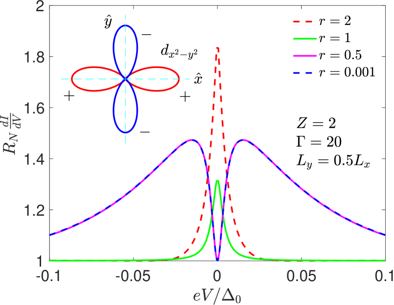
Next, we consider and states which possess anisotropic orbital components. For the state, and are modeled by . For this gap function, there are two line nodes at an angle w.r.t. the interface normal axis. Since we have already shown that a T-shaped junction with shorter leg length is better for observing the ZBCP, we fix the value of at and consider a good quality interface with and for our differential conductance calculations with anisotropic form factors. Fig. 4 shows the differential conductance for a T-shaped junction attached to symmetry superconductor. We find qualitatively similar behavior for a superconductor to that of a superconductor which was discussed above. This qualitative similarity between and superconductors can be understood by examining the phase shift in the gap functions of incoming and outgoing quasiparticle trajectories at the interface. For the orbital function, the incoming and the outgoing are qualitatively the same as superconductor. The nodal line of the form factor is at an angle of , so there is no additional sign change due to this anisotropic factor, and the triplet component is effectively the same as for the superconductor. However, the form factor reduces the height of the ZBCP in the triplet dominated regime (), and in the strong singlet regime , the tiny peak that we find for the superconductors is smeared and the lineshape is similar to a wave superconductor.
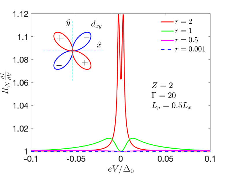
In contrast, we find a qualitatively different behavior for the state, as shown in the Fig. 5, there is a splitting of the ZBCP with reduced heights. For a orbital factor, the nodal line is along the interface normal, therefore for all the incoming gap functions form factor gives a sign change to the outgoing gap function. The triplet component has an additional chiral -wave factor, which also gives a sign change between incoming and outgoing gap functions, which gets canceled by the sign change from the factor, hence there is no overall sign change. This is qualitatively equivalent to an extended wave state. For triplet dominant cases, a ZBCP with splitting is the outcome of this lack of sign change. In case of a -wave superconductor, two opposite contributions to the conductivity exist: while the loss of density of states reduces the conductivity, Maki-Thompson like processes result in an enhancement. For isotropic -wave systems, these two effects cancel at zero energy. However, the additional anisotropy from the orbital form factor may not give an exact cancellation, this could lead to an increased conductivity at the zero energy in comparison with a pure isotropic wave superconductor. In the limit of strong singlet component, we find a featureless conductivity. This is expected because the nodal line in parallel to the interface normal, and in such orientation no proximity effect occurAsano (2001).
Concluding Remarks–In this paper, we have studied the conductance of T-shaped junctions connected to a superconductor under the influence of a strong Rashba SOC generated by the underlying substrate. The vector in the superconducting state is determined by the SOC. The superconducting state is a mixed parity state with both singlet and triplet components. We calculated the tunneling conductance for this system within the quasiclassical formalism. The effect of the superconducting order is included through Nazarov-Tanaka boundary conditions. We looked at the effect of the device size on the zero-bias conductance peak. In agreement with earlier work, we find that smaller device dimensions result in larger FWHM of the ZBCPs. Moreover, we showed that both triplet and singlet components affect the conductance.
Specifically, we considered , and pairing states. The and states produce ZBCPs, whenever the triplet component is stronger than the singlet one. The peak is weaker in the case of superconductors due to anisotropic orbital form factor. In the strong singlet limit, we find a dip structure in the conductance spectrum. For the state, in the regime where a finite but small triplet component co-exists with a large singlet component, we predict a weak ZBCP on top of the dip structure. This ZBCP disappears quickly with the decreasing triplet strength. For the state, the weak ZBCP disappears rapidly already when the triplet component becomes smaller than the singlet component. In contrast, we find a ZBCP splitting for the state, which happens because the triplet component does not cause a sign change of the incoming and outgoing gaps. Thus, we conclude that making interfaces with different crystallographic orientations of the superconductor will be useful for drawing concrete conclusions in systems, where anisotropic orbital form factors are likely to be present.
In the context of the recent experimental results on \ceCoSi2/\ceTiSi2 heterostructuresChiu et al. (2020), we believe that the state is consistent with the experiments. We have performed our calculations for device sizes that are comparable to the experimental setup. We found that in the triplet dominant regime, the opposite chirality superconductivity on the two helical bands gives a ZBCP in the conductance of the T-junction. This peak is quite robust and stronger than the peak expected for a usual chiral wave superconductorAsano et al. (2007). Therefore, we think that the \ceCoSi2/\ceTiSi2 heterostructure is a triplet dominant () superconductor. The conductance for an SN junction comprised of such a triplet dominant mixed parity superconductor and a normal metal junction has been studied earlierIniotakis et al. (2007), and agrees with the \ceCoSi2/\ceTiSi2 tunnel junction data barring the sharp feature at the zero energy.
One of the major issue with our description of the \ceCoSi2/\ceTiSi2 heterostructures is the lack of the time reversal symmetry breaking (TRSB) that has been observed up to . The TRSB in the mixed parity superconductors has been predicted earlier,Timm et al. (2015); Wang and Fu (2017) however it is expected to happen at a lower temperature below . Twin boundaries can also cause TRSB, if the triplet and the singlet components are comparable in magnitudesArahata et al. (2013). Another possible explanation for the hysteresis observed in the magnetoresistance data is the Zeeman field induced supercurrent. In a superconductor with broken inversion symmetry, an in-plane Zeeman field gives rise to a supercurrent flow along the direction perpendicular to itYip (2002); Edelstein (2003). We think that SR experiments on \ceCoSi2/\ceTiSi2 heterostructures will provide an ubiquitous evidence for TRSB.
We have considered a simple one band model for the \ceCoSi2 for qualitatively understanding the \ceCoSi2/\ceTiSi2 heterostructures. However, it is a multiband system, which can be a possible origin of the TRSB. We leave this issue of TRSB for future study. We conclude that the \ceCoSi2/\ceTiSi2 heterostructure is a mixed parity superconducting state with a dominant wave component. Such mix parity superconductor with a dominant triplet component is a topologically nontrivial system and is similar to a quantum spin hall systemTanaka et al. (2009); Sato and Fujimoto (2009). It hosts topologically protected Andreev bound states, which carry spin currents, therefore constituting an important platform for further research.
Acknowledgments
The authors are grateful to Shao-Pin Chiu and Juhn-Jong Lin for helpful discussions. VM, YL and FCZ are partially supported by NSFC grant 11674278 and by the priority program of the Chinese Academy of Sciences grant No. XDB28000000, and by the China Postdoctoral Science Foundation under grant No. 2020M670422 (YL). Work at Zhejiang University was in part supported by the National Key R&D Program of the MOST of China, grant No. 2016YFA0300202 and the National Science Foundation of China, grant No. 11774307.
References
- Read and Green (2000) N. Read and D. Green, Phys. Rev. B 61, 10267 (2000).
- Kitaev (2001) A. Y. Kitaev, Physics-Uspekhi 44, 131 (2001).
- Ivanov (2001) D. A. Ivanov, Phys. Rev. Lett. 86, 268 (2001).
- Kitaev (2003) A. Kitaev, Annals of Physics 303, 2 (2003).
- Wilczek (2009) F. Wilczek, Nature Physics 5, 614 (2009).
- Nayak et al. (2008) C. Nayak, S. H. Simon, A. Stern, M. Freedman, and S. Das Sarma, Rev. Mod. Phys. 80, 1083 (2008).
- Lutchyn et al. (2010) R. M. Lutchyn, J. D. Sau, and S. Das Sarma, Phys. Rev. Lett. 105, 077001 (2010).
- Oreg et al. (2010) Y. Oreg, G. Refael, and F. von Oppen, Phys. Rev. Lett. 105, 177002 (2010).
- Mourik et al. (2012) V. Mourik, K. Zuo, S. M. Frolov, S. R. Plissard, E. P. A. M. Bakkers, and L. P. Kouwenhoven, Science 336, 1003 (2012).
- Nadj-Perge et al. (2014) S. Nadj-Perge, I. K. Drozdov, J. Li, H. Chen, S. Jeon, J. Seo, A. H. MacDonald, B. A. Bernevig, and A. Yazdani, Science 346, 602 (2014).
- Volovik (2003) G. E. Volovik, The Universe in a Helium Droplet (Oxford University Pres, 2003).
- Wang et al. (2018) D. Wang, L. Kong, P. Fan, H. Chen, S. Zhu, W. Liu, L. Cao, Y. Sun, S. Du, J. Schneeloch, R. Zhong, G. Gu, L. Fu, H. Ding, and H.-J. Gao, Science 362, 333 (2018).
- Liu et al. (2018) Q. Liu, C. Chen, T. Zhang, R. Peng, Y.-J. Yan, C.-H.-P. Wen, X. Lou, Y.-L. Huang, J.-P. Tian, X.-L. Dong, G.-W. Wang, W.-C. Bao, Q.-H. Wang, Z.-P. Yin, Z.-X. Zhao, and D.-L. Feng, Phys. Rev. X 8, 041056 (2018).
- Fu and Kane (2008) L. Fu and C. L. Kane, Phys. Rev. Lett. 100, 096407 (2008).
- Sun et al. (2016) H.-H. Sun, K.-W. Zhang, L.-H. Hu, C. Li, G.-Y. Wang, H.-Y. Ma, Z.-A. Xu, C.-L. Gao, D.-D. Guan, Y.-Y. Li, C. Liu, D. Qian, Y. Zhou, L. Fu, S.-C. Li, F.-C. Zhang, and J.-F. Jia, Phys. Rev. Lett. 116, 257003 (2016).
- Mackenzie and Maeno (2003) A. P. Mackenzie and Y. Maeno, Rev. Mod. Phys. 75, 657 (2003).
- Asano et al. (2007) Y. Asano, Y. Tanaka, A. A. Golubov, and S. Kashiwaya, Phys. Rev. Lett. 99, 067005 (2007).
- Chiu et al. (2020) S.-P. Chiu, C. C. Tsuei, S.-S. Yeh, F.-C. Zhang, S. Kirchner, and J.-J. Lin, Observation of triplet superconductivity in \ceCoSi2/\ceTiSi2 heterostructures (2020), arXiv:2012.13679 .
- Blonder et al. (1982) G. E. Blonder, M. Tinkham, and T. M. Klapwijk, Phys. Rev. B 25, 4515 (1982).
- Matthias (1952) B. T. Matthias, Phys. Rev. 87, 380 (1952).
- Mattheiss and Hamann (1988) L. F. Mattheiss and D. R. Hamann, Phys. Rev. B 37, 10623 (1988).
- Tsutsumi et al. (1997) K. Tsutsumi, S. Takayanagi, and T. Hirano, Physica B: Condensed Matter 237-238, 310 (1997), proceedings of the Yamada Conference XLV, the International Conference on the Physics of Transition Metals.
- Gor’kov and Rashba (2001) L. P. Gor’kov and E. I. Rashba, Phys. Rev. Lett. 87, 037004 (2001).
- Iniotakis et al. (2007) C. Iniotakis, N. Hayashi, Y. Sawa, T. Yokoyama, U. May, Y. Tanaka, and M. Sigrist, Phys. Rev. B 76, 012501 (2007).
- Vorontsov et al. (2008) A. B. Vorontsov, I. Vekhter, and M. Eschrig, Phys. Rev. Lett. 101, 127003 (2008).
- Tanaka et al. (2010) Y. Tanaka, Y. Mizuno, T. Yokoyama, K. Yada, and M. Sato, Phys. Rev. Lett. 105, 097002 (2010).
- Eschrig et al. (2012) M. Eschrig, C. Iniotakis, and Y. Tanaka, Non-Centrosymmetric Superconductors, edited by E. Bauer and M. Sigrist, Lecture Notes in Physics, Vol. 847 (Springer Berlin Heidelberg, 2012) pp. 313–357.
- Tamura and Tanaka (2019) S. Tamura and Y. Tanaka, Phys. Rev. B 99, 184501 (2019).
- Tada et al. (2008) Y. Tada, N. Kawakami, and S. Fujimoto, Journal of the Physical Society of Japan 77, 054707 (2008).
- Yanase and Sigrist (2008) Y. Yanase and M. Sigrist, Journal of the Physical Society of Japan 77, 124711 (2008).
- Usadel (1970) K. D. Usadel, Phys. Rev. Lett. 25, 507 (1970).
- Hayashi et al. (2006) N. Hayashi, K. Wakabayashi, P. A. Frigeri, and M. Sigrist, Phys. Rev. B 73, 092508 (2006).
- Frigeri et al. (2004) P. A. Frigeri, D. F. Agterberg, A. Koga, and M. Sigrist, Phys. Rev. Lett. 92, 097001 (2004).
- Frigeri et al. (2005) P. A. Frigeri, D. F. Agterberg, I. Milat, and M. Sigrist, arXiv e-prints , cond-mat/0505108 (2005), arXiv:cond-mat/0505108 [cond-mat.supr-con] .
- Annunziata et al. (2012) G. Annunziata, D. Manske, and J. Linder, Phys. Rev. B 86, 174514 (2012).
- Zaitsev (1994) A. Zaitsev, Physics Letters A 194, 315 (1994).
- Nazarov (1999) Y. V. Nazarov, Superlattices and Microstructures 25, 1221 (1999).
- Tanaka et al. (2003) Y. Tanaka, Y. V. Nazarov, and S. Kashiwaya, Phys. Rev. Lett. 90, 167003 (2003).
- Tanaka et al. (2004a) Y. Tanaka, Y. V. Nazarov, A. A. Golubov, and S. Kashiwaya, Phys. Rev. B 69, 144519 (2004a).
- Tanaka et al. (2004b) Y. Tanaka, Y. V. Nazarov, A. A. Golubov, and S. Kashiwaya, Phys. Rev. B 70, 219907 (2004b).
- Tanaka et al. (2005a) Y. Tanaka, Y. Asano, A. A. Golubov, and S. Kashiwaya, Phys. Rev. B 72, 140503 (2005a).
- Tanaka et al. (2006a) Y. Tanaka, Y. Asano, A. A. Golubov, and S. Kashiwaya, Phys. Rev. B 73, 059901 (2006a).
- Morten et al. (2005) J. P. Morten, A. Brataas, and W. Belzig, Phys. Rev. B 72, 014510 (2005).
- Tanaka et al. (2005b) Y. Tanaka, Y. Asano, A. A. Golubov, and S. Kashiwaya, Phys. Rev. B 72, 140503 (2005b).
- Tanaka et al. (2006b) Y. Tanaka, Y. Asano, A. A. Golubov, and S. Kashiwaya, Phys. Rev. B 73, 059901 (2006b).
- Tanaka and Golubov (2007) Y. Tanaka and A. A. Golubov, Phys. Rev. Lett. 98, 037003 (2007).
- Volkov and Takayanagi (1996) A. F. Volkov and H. Takayanagi, Phys. Rev. Lett. 76, 4026 (1996).
- Volkov and Takayanagi (1997) A. F. Volkov and H. Takayanagi, Phys. Rev. B 56, 11184 (1997).
- Asano (2001) Y. Asano, Phys. Rev. B 64, 014511 (2001).
- Timm et al. (2015) C. Timm, S. Rex, and P. M. R. Brydon, Phys. Rev. B 91, 180503 (2015).
- Wang and Fu (2017) Y. Wang and L. Fu, Phys. Rev. Lett. 119, 187003 (2017).
- Arahata et al. (2013) E. Arahata, T. Neupert, and M. Sigrist, Phys. Rev. B 87, 220504 (2013).
- Yip (2002) S. K. Yip, Phys. Rev. B 65, 144508 (2002).
- Edelstein (2003) V. M. Edelstein, Phys. Rev. B 67, 020505 (2003).
- Tanaka et al. (2009) Y. Tanaka, T. Yokoyama, A. V. Balatsky, and N. Nagaosa, Phys. Rev. B 79, 060505 (2009).
- Sato and Fujimoto (2009) M. Sato and S. Fujimoto, Phys. Rev. B 79, 094504 (2009).