Identification of the Nitrogen Interstitial as Origin of the 3.1 eV Photoluminescence Band in Hexagonal Boron Nitride
Abstract
Nitrogen interstitials (N) have the lowest formation energy among intrinsic defects of hexagonal boron nitride (hBN) under n-type and N-rich conditions. Using an optimized hybrid functional, which reproduces the gap and satisfies the generalized Koopmans condition, an N configuration is found which is lower in energy than the ones reported so far. The (0/-) charge transition level is also much deeper, so N acts as a very efficient compensating center in n-type samples. Its calculated photoluminescence (PL) at 3.0 eV agrees well with the position of an N-sensitive band measured at 3.1 eV. It has been also found that the nitrogen vacancy (V) cannot be the origin of the three boron electron (TBC) electron paramagnetic resonance (EPR) center and in thermal equilibrium it cannot even exist in n-type samples.
Elham Khorasani, Thomas Frauenheim, Bálint Aradi* and Peter Deák*
Elham Khorasani
Bremen Center for Computational Materials Science, University of Bremen,
P.O. Box 330440, D-28334 Bremen, Germany.
Prof. Dr. Thomas Frauenheim
Beijing Computational Science Research Center (CSRC), 100193 Beijing, China.
Shenzhen JL Computational Science and Applied Research Institute, 518110
Shenzhen, China.
Bremen Center for Computational Materials Science, University of Bremen,
P.O. Box 330440, D-28334 Bremen, Germany.
Dr. Bálint Aradi
Bremen Center for Computational Materials Science, University of Bremen,
P.O. Box 330440, D-28334 Bremen, Germany.
Email Address: aradi@uni-bremen.de
Prof. Dr. Peter Deák
Bremen Center for Computational Materials Science, University of Bremen,
P.O. Box 330440, D-28334 Bremen, Germany.
Email Address: peter.deak@bccms.uni-bremen.de
1 Introduction
Materials with well-defined defect centers are highly promising for next generation devices, with applications ranging from electronics and photonics to quantum computing [1, 2]. Hexagonal boron nitride (hBN) is a wide-band-gap semiconductor that exhibits a rich number of band gap levels which profoundly impact its electronic and optical properties. These can act as recombination centers and emit light within a specific energy range. In recent years, numerous color centers have been reported in hBN [3, 4]. However, the physical origin of some of these centers is not yet fully understood [5, 6]. First principle calculations can play a crucial role in identifying the defects and providing accurate information about their properties.
The luminescence properties of hBN have been studied mainly in recent years [5, 7, 8, 9, 10]. Museur et al. reported three photoluminescence (PL) bands at the energies of 5.3 eV, 3.75 eV, and 3.1 eV for pyrolytic hBN (pBN) samples [7]. pBN samples are high purity samples, free of carbon and oxygen. The emission bands around 5.3 eV and 3.57 eV were found to be donor-acceptor pair (DAP) type transitions. The nature of the PL band observed at 3.1 eV in pBN samples was not elucidated. Du et al. [8] investigated the PL spectra for a set of hBN epilayers grown by metal organic chemical vapor deposition (MOCVD) under different ammonia () flow rates from 0.2 to 1.5 standard liters per minute (SLM). They observed four emission peaks at energies of 4.12 eV, 3.92 eV, 3.72 eV, and 5.37 eV for hBN under the flow rate of 0.2 SLM. The first three peaks were interpreted as a zero phonon line at 4.12 eV with two phonon replicas. They observed a decrease in the emission intensity for the peak at 4.12 eV upon increasing the flow rate while the change of the peak at 5.37 eV was found to be small. They also observed the appearance of the peak at 3.1 eV as the flow rate of the was increased to 1.5 SLM.
Besides PL spectroscopy, electron paramagnetic resonance (EPR) is a powerful technique often used for identifying and studying defects in semiconductors and insulators [11]. Two types of paramagnetic centers were identified in hBN [6, 12, 13, 14]. In one type, an unpaired electron interacts with three equivalent boron nuclei, producing a 10-line EPR spectrum. This type is referred to as the three boron center (TBC). In another type, an unpaired electron interacts with a single boron nucleus, which gives rise to a 4-line EPR spectrum. This is referred to as the one boron center (OBC). Based on experimental observation, the carbon substitutional () and the nitrogen vacancy () were proposed [6, 14, 15] to model the TBC. In the former, an unpaired electron was trapped at the carbon atom. This was referred to as a carbon-associated TBC and was confirmed theoretically [15]. In the model, proposed by experiments [6], the unpaired electron is assumed to be trapped in the nitrogen vacancy. This was referred to as an electron-irradiation produced TBC. However, its nature is still controversial.
We have applied an optimized hybrid functional to calculate defects in hBN. Our calculations show that the observed PL at 3.1 eV in bulk hBN is due to the recombination of an electron with a hole trapped at a nitrogen interstitial, . Additionally, we have found that cannot be the origin of the TBC center. In fact, in n-type samples in equilibrium, turns out to be less stable than even under extreme N-poor conditions, indicating that can be created only by irradiation.
2 Computational method
It was shown that the screened hybrid functional of Heyd, Scuseria, and Ernzerhof (HSE) [16, 17], with parameters tuned to reproduce the relative position of the quasi-particle band edges and to satisfy the generalized Koopman’s theorem (gKT), is capable of providing the formation energy, the charge transition levels and the hyperfine interaction of defects very accurately in traditional bulk semiconductors [18, 19, 20]. In our previous work, we have shown that such a functional can be optimized for layered compounds as well [21] and HSE() with a mixing parameter = 0.3 and a screening parameter = 0.4 was found as the optimal functional for bulk hBN.
Our calculations in the present work have been carried out with the Vienna Ab initio Simulation Package, VASP 5.4.4, using the projector augmented wave method [22, 23, 24]. A 420 (840) eV cutoff was applied for the expansion of the wave functions (charge density) in hBN. The convergence condition of 10-4 eV was applied for the self-consistent electronic energy. Van der Waals interactions between the layers were taken into account by the Tkatchenko-Scheffler method [25], using = 0.96.
The equilibrium geometry was determined for the primitive unit cell with a -centered Monkhorst-Pack (MP) -point set [26], based on constant volume relaxations and fitting to Murnaghan’s equation of state [27]. We describe bulk hBN using an orthogonal supercell of 120 atoms (5a1, 3a1 + 6a2, a3) at the calculated lattice constants (see our previous work [21]), using the -point approximation. (Here , , and are the primitive unit vectors). The geometries of the defects in the supercell were relaxed at fixed lattice constants, using a force criterion of 0.01 eV/Å.
We have calculated the formation energy and the transition levels of the intrinsic defects and . The chemical potentials and are related in equilibrium, as where is the energy of hBN per formula unit. For N-rich conditions the chemical potential of nitrogen was taken as the energy of the nitrogen atom in the molecule (at a temperature of 300 K and a pressure of 105 Pa). For the B-rich case corresponds to the energy of the B atom in the solid phase. For charged defects, total energies were corrected a posteriori, using the SLABCC code [28, 29] to eliminate the artificial interaction between the repeated charges. SLABCC is based on the scheme proposed by Komsa and Pasquarello [30]. For the correction, the static dielectric constant should be used in principle if the ionic cores are allowed to relax. However, it was shown that, due to the explicit screening in the supercell, the high-frequency value gives a better approximation [31], therefore and [32] were used.
To explain the observed PL in bulk hBN, we have investigated electron recombination with a hole trapped at . Within the accuracy of the calculation (0.1 eV), a shallow donor state cannot be distinguished energetically from the bottom of the conduction band. Therefore, we simulate a donor-acceptor recombination from a shallow donor to a deep acceptor by the recombination of a bound exciton, i.e., from the conduction band edge to the acceptor level [8]. To calculate the PL, we first relaxed the equilibrium geometry of the bound exciton under the constraint of the orbital occupations, i.e., with one hole at the defect level and with one electron in the conduction band minimum (CBM). To consider the delocalization of the electron, the total energy of the initial state was recalculated with a (non--centered) Monkhorst-Pack set at the relaxed geometry of the bound exciton in the approximation. The energy of the final state after recombination was calculated at fixed geometry, using the same -point set. The PL energy is the difference between the two total energies.
Hyperfine interaction was calculated for . Boron has two isotopes, and , with the natural abundances of and , respectively. These isotopes have different nuclear spins and magnetic moments. In this work, the hyperfine splitting was compared to the experimental data measured in -enriched samples. The presented results were obtained for the isotope with . The nuclear gyromagnetic ratios of 13.66 and 3.08 were used for boron and nitrogen, respectively [33].
3 Results and Discussion
3.1 Nitrogen interstitial
In earlier works, the nitrogen interstitial was predicted to be in a [001] split interstitial configuration with a lattice N atom [34, 35], and was found to be the intrinsic defect with the lowest formation energy under N-rich conditions in n-type material. We have found, however, that the configuration shown in Figure 1 is lower in energy by 0.70 eV. The axis of the split interstitial tilts away from [001], so both nitrogen atoms are ideally threefold coordinated. The - bondlength, 1.38 Å corresponds to a single bond, and also binds to a boron atom of the top layer. Simple electron counting shows that the -orbital of , which is orthogonal to the plane of its three bonds, contains only one electron.
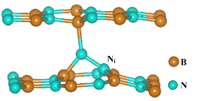
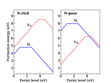
Figure 2 shows the formation energy calculated for the intrinsic defects and in different charge states, as a function of the Fermi level position between the valence band maximum (VBM) and the conduction band minimum (CBM). The adiabatic charge transition levels for are obtained at 0.94 eV and 2.68 eV with respect to the valence band edge. The latter is much deeper than the value obtained in a previous work [34]. Weston et al. predicted to be the major compensating center in n-type samples [34]. Our finding confirms that and the lower formation energy indicates an even stronger compensating effect.
3.2 Nitrogen Vacancy
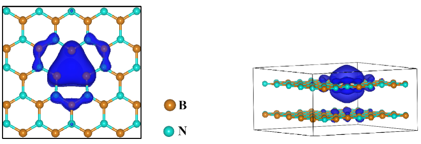
The similarities between optical emitters in hBN and the nitrogen-vacancy () center in diamond, have brought a lot of attention to vacancy defects in hBN. Earlier experimental studies proposed as the source of the TBC [6], which was produced by electron irradiation. introduces a gap level with an unpaired electron. Our calculations show that the electron is on -orbitals orthogonal to the lattice planes, with a symmetrical charge distribution on the three neighboring boron atoms. Figure 3 shows the spin distribution. The calculated hyperfine coupling constants are given in Table 1. The calculated average principle value of the hyperfine interaction tensor is obtained at 34.23 MHz, which is significantly smaller than the value of 117.06 MHz measured for the TBC in carbon-free samples after irradiation. It has been shown that core spin polarization may have a significant effect on the hyperfine interaction calculated, providing accurate results in various semiconductors [36]. Taking the core contribution into account, the calculated magnitude of 34.23 MHz, which only involved the valence electronic spin density, reduced to 16.09 MHz, demonstrating that the can not be the origin of the three boron center.
The nitrogen instersitial defect, is expected to be more stable than in N-rich samples. This is also confirmed by Figure 2. However, as demonstrated by the same figure, even under extreme N-poor conditions, can only exist in p-type samples in thermal equilibrium. Actually, there is no hard experimental evidence for the existence of . In the earlier PL studies [5, 8, 9, 37], the nitrogen vacancy was suggested as a possible source of the 4.1 eV emission band in bulk hBN. Later on, however, a theoretical study showed that the carbon dimer defect is responsible for the 4.1 eV emission in hBN [38]. Jin et al. [39] used ultrahigh-resolution transmission electron microscope imaging. They created defects by an electron beam irradiation and found that the created defects are of the boron vacancy () type.
| (experimental)111andrei1976point | ||||
|---|---|---|---|---|
| 21.21 | 20.81 | 60.65 | 34.23 | 117.06 |
4 Conclusion
We have calculated the intrinsic defects, nitrogen interstitial and nitrogen vacancy, using the optimal HSE (0.4, 0.3) functional for hBN as obtained in our previous work. We have found an configuration which is considerably lower in energy than the ones reported so far. The calculated formation energies show that is the intrinsic defect with the lowest formation energy under N-rich conditions. Its acceptor level is deep and behaves as a compensating center. The calculated PL energy of 3.0 eV for is in good agreement with the experimentally observed N-related band at 3.1 eV [7, 8]. We have investigated the nitrogen vacancy as well. Our result indicates that is less stable than in n-type samples even under extreme N-poor conditions and should be observable only in irradiated samples. The hyperfine interactions have been calculated for , which was suspected to be a source of the three boron centers produced under an electron-irradiation in carbon-free samples. Our results indicate that cannot be the origin of the three boron center in bulk hBN.
Acknowledgements
This work was supported by the Deutsche Forschungsgemeinschaft (DFG) within the research training group (RTG) 2247.
References
- [1] V. Ivády, G. Barcza, G. Thiering, S. Li, H. Hamdi, J.-P. Chou, Ö. Legeza, A. Gali, npj Comput. Mater. 2020, 6, 1 1.
- [2] S. Kim, J. E. Fröch, J. Christian, M. Straw, J. Bishop, D. Totonjian, K. Watanabe, T. Taniguchi, M. Toth, I. Aharonovich, Nat. Commun. 2018, 9, 1 1.
- [3] T. T. Tran, C. Elbadawi, D. Totonjian, C. J. Lobo, G. Grosso, H. Moon, D. R. Englund, M. J. Ford, I. Aharonovich, M. Toth, ACS Nano 2016, 10, 8 7331.
- [4] D. Wong, J. Velasco, L. Ju, J. Lee, S. Kahn, H.-Z. Tsai, C. Germany, T. Taniguchi, K. Watanabe, A. Zettl, et al., Nat. Nanotechnol. 2015, 10, 11 949.
- [5] L. Museur, E. Feldbach, A. Kanaev, Phys. Rev. B 2008, 78, 15 155204.
- [6] E. Andrei, A. Katzir, J. Suss, Phys. Rev. B 1976, 13, 7 2831.
- [7] L. Museur, A. Kanaev, J. Mater. Sci. 2009, 44, 10 2560.
- [8] X. Du, J. Li, J. Lin, H. Jiang, Appl. Phys. Lett. 2015, 106, 2 021110.
- [9] M. Silly, P. Jaffrennou, J. Barjon, J.-S. Lauret, F. Ducastelle, A. Loiseau, E. Obraztsova, B. Attal-Tretout, E. Rosencher, Phys. Rev. B 2007, 75, 8 085205.
- [10] T. Vuong, G. Cassabois, P. Valvin, A. Ouerghi, Y. Chassagneux, C. Voisin, B. Gil, Phys. Rev. Lett. 2016, 117, 9 097402.
- [11] G. D. Watkins, Identification of Defects in Semiconductors and Semimetals, volume 51A, Academic Press, San Diego, edited by m. stavola edition, 1999.
- [12] D. Geist, G. Römelt, Solid State Commun. 1964, 2, 5 149.
- [13] A. Katzir, J. Suss, A. Zunger, A. Halperin, Phys. Rev. B 1975, 11, 6 2370.
- [14] A. Moore, L. Singer, J. Phys. Chem. Solids 1972, 33, 2 343.
- [15] A. Sajid, J. R. Reimers, M. J. Ford, Phys. Rev. B 2018, 97, 6 064101.
- [16] J. Heyd, G. E. Scuseria, M. Ernzerhof, J. Chem. Phys. 2003, 118, 18 8207.
- [17] J. Heyd, G. E. Scuseria, M. Ernzerhof, J. Chem. Phys. 2006, 124, 21 219906.
- [18] P. Deák, M. Lorke, B. Aradi, T. Frauenheim, J. Appl. Phys 2019, 126, 13 130901.
- [19] P. Deák, Q. D. Ho, F. Seemann, B. Aradi, M. Lorke, T. Frauenheim, Phys. Rev. B 2017, 95, 7 075208.
- [20] M. Han, Z. Zeng, T. Frauenheim, P. Deák, Phys. Rev. B 2017, 96, 16 165204.
- [21] P. Deák, E. Khorasani, M. Lorke, M. Farzalipour-Tabriz, B. Aradi, T. Frauenheim, Phys. Rev. B 2019, 100, 23 235304.
- [22] G. Kresse, J. Hafner, Phys. Rev. B 1994, 49, 20 14251.
- [23] G. Kresse, J. Furthmüller, Phys. Rev. B 1996, 54, 16 11169.
- [24] G. Kresse, D. Joubert, Phys. Rev. B 1999, 59, 3 1758.
- [25] A. Tkatchenko, M. Scheffler, Phys. Rev. Lett. 2009, 102 073005.
- [26] H. J. Monkhorst, J. D. Pack, Phys. Rev. B 1976, 13, 12 5188.
- [27] F. D. Murnaghan, PNAS 1944, 30, 9 244.
- [28] M. F. Tabriz, B. Aradi, T. Frauenheim, P. Deák, Comp. Phys. Comm. 2019, 240 101.
- [29] M. Farzalipour, SLABCC: Total energy correction code for charged periodic slab models, Source code can be downloaded from https://github.com/MFTabriz/slabcc.
- [30] H.-P. Komsa, N. Berseneva, A. V. Krasheninnikov, R. M. Nieminen, Phys. Rev. X 2014, 4 031044.
- [31] P. Deák, Q. Duy Ho, F. Seemann, B. Aradi, M. Lorke, T. Frauenheim, Phys. Rev. B 2017, 95 075208.
- [32] R. Geick, C. Perry, G. Rupprecht, Phys. Rev. 1966, 146, 2 543.
-
[33]
NMR Periodic Table,
Data are gotten from:
http://www-usr.rider.edu/grushow/nmr/NMR-tutor/periodic-table/nmr-pt-frameset.html. - [34] L. Weston, D. Wickramaratne, M. Mackoit, A. Alkauskas, C. G. Van de Walle, Phys. Rev. B 2018, 97 214104.
- [35] V. Wang, R.-J. Liu, H.-P. He, C.-M. Yang, L. Ma, Solid State Commun. 2014, 177 74.
- [36] K. Szász, T. Hornos, M. Marsman, A. Gali, Phys. Rev. B 2013, 88 075202.
- [37] K. Watanabe, T. Taniguchi, H. Kanda, Nat. Mater. 2004, 3, 6 404.
- [38] M. Mackoit-Sinkevičienė, M. Maciaszek, C. G. Van de Walle, A. Alkauskas, Appl. Phys. Lett. 2019, 115, 21 212101.
- [39] C. Jin, F. Lin, K. Suenaga, S. Iijima, Phys. Rev. Lett. 2009, 102, 19 195505.