Dissipative Transport and Phonon Scattering Suppression via Valley Engineering in Single-Layer Antimonene and Arsenene Field-Effect Transistors
Abstract
Two-dimensional (2D) semiconductors are promising channel materials for next-generation field-effect transistors (FETs) thanks to their unique mechanical properties and enhanced electrostatic control. However, the performance of these devices can be strongly limited by the scattering processes between carriers and phonons, usually occurring at high rates in 2D materials. Here, we use quantum transport simulations calibrated on first-principle computations to report on dissipative transport in antimonene and arsenene -type FETs at the scaling limit. We show that the widely-used approximations of either ballistic transport or simple acoustic deformation potential scattering result in large overestimation of the ON current, due to neglecting the dominant intervalley and optical phonon scattering processes. We additionally investigate valley engineering strategy [Nano Lett. 19, 3723 (2019)] to improve the device performance by removing the valley degeneracy and suppressing most of the intervalley scattering channels via an uniaxial strain along the zigzag direction. The method is applicable to other similar 2D semiconductors characterized by multivalley transport.
I Introduction
Recently, two-dimensional (2D) materials have shown a wealth of interesting properties and possible technological applications Fiori et al. (2014); Novoselov et al. (2016); Schaibley et al. (2016); Yang, Jiang, and Wei (2017); Jin et al. (2018); Liu and Hersam (2019); Das et al. (2019); Zhang et al. (2018). Their mechanical properties, ultimate thinness and absence of surface dangling bonds are particularly suitable for conventional and flexible electronics Fiori et al. (2014); Radisavljevic et al. (2011); Wang et al. (2012); Chhowalla, Jena, and Zhang (2016); Cao et al. (2016); Pizzi et al. (2016); Polyushkin et al. (2020). The 2D materials with a finite energy bandgap have the potential to replace Si as the channel material in ultra-scaled metal-oxide-semiconductor field-effect transistors (MOSFETs) for future nanoelectronics Radisavljevic et al. (2011); Fiori et al. (2014). However, two main issues hinder the adoption of 2D materials for MOSFET applications, namely the high resistance between metallic contacts and semiconducting 2D materials Allain et al. (2015) and their relatively low mobility.
Experimental measurements of room temperature electron mobilities in 2D materials have so far reported values lower than 400 cm2V-1s-1, Radisavljevic et al. (2011); Allain and Kis (2014); Li et al. (2014); Liu et al. (2018); Sohier et al. (2018) much smaller than the value for bulk Si (about 1400 cm2V-1s-1) Cheng, Zhang, and Liu (2020); Poncé, Margine, and Giustino (2018). When employed in electron devices in place of 3D semiconductors such as Si, Ge and III-V compounds, 2D-material-based MOSFETs do not suffer from surface roughness scattering Poli et al. (2008); Grillet et al. (2017), but have a room-temperature mobility limited by defects and electron-phonon coupling (EPC). The former, just as the contact resistance, can in principle be reduced by developing dedicated engineering processes Liao et al. (2020). On the contrary, the electron-phonon scattering represents an intrinsic mechanism and cannot be easily suppressed at room temperature.
Unfortunately, 2D semiconductors usually have larger electron-phonon scattering rates with respect to their 3D counterparts, due to a higher density of electronic and phononic states at energies close to the band extrema Cheng, Zhang, and Liu (2020). The low phonon-limited mobility in monolayers has been also confirmed by several first-principle calculations based on density functional theory (DFT) and on the Boltzmann transport equation Kaasbjerg, Thygesen, and Jacobsen (2012); Sohier et al. (2018); Liu and Hersam (2019); Fischetti and Vandenberghe (2016); Sohier, Calandra, and Mauri (2016); Cheng and Liu (2018); Cheng, Zhang, and Liu (2019).
In light of these considerations, it appears compulsory to take into account the electron-phonon interactions in the simulation of 2D material-based electron devices, in order to obtain reliable quantitative predictions of the device performance at room temperature. Nevertheless, only a few recent simulation studies have fully included the effect of EPC Szabó, Rhyner, and Luisier (2015); Logoteta et al. (2020). In other works, the mobility has been evaluated through the Takagi formula Takagi et al. (1994), which takes into account only the Bardeen-Shockley acoustic-deformation-potential (ADP) scattering Bardeen and Shockley (1950) and neglects all the optical and intervalley phonon scatterings Wang et al. (2017); Pizzi et al. (2016). However, many 2D semiconductors have multiple degenerate conduction band valleys, which results in a large phase space for intervalley scatterings and in large scattering rates Sohier et al. (2018, 2019). The inelastic nature of these scattering processes has been already shown to deeply affect the transport in electronic devices Szabó, Rhyner, and Luisier (2015); Pala et al. (2016).
More often, only the ballistic regime is considered in simulations. This approximation is usually justified by invoking the shortness of the considered device, though no experimental evidence of ballistic transport at room temperature for 2D materials other than graphene has been provided yet. Therefore, it is still unclear to which extent the electron-phonon scattering affects the room-temperature transport even in devices with characteristic lengths of less than ten nanometers.
In this paper, we report the results of room-temperature numerical simulations of arsenene- and antimonene-based short-channel MOSFETs with double-gate architecture. Arsenene and antimonene are among the most promising candidates as channel materials in emerging MOSFET devices, due to their small effective masses and correspondingly high theoretical mobility Wang et al. (2017); Pizzi et al. (2016); Klinkert et al. (2020). However, previous application-oriented studies have been based either on purely ballistic simulations or have considered only acoustic phonon scattering. A full treatment of EPC in these materials is therefore still missing.
To this purpose, we use a non-equilibrium Green’s function (NEGF) transport solver including acoustic and optical intra- and intervalley EPCs with parameters fully determined from first-principles calculations. The NEGF transport solver is coupled with a Poisson solver for self-consistently computing the electrostatic potential in the whole device domain.
The main findings of this work are not limited to the specific case of arsenene and antimonene, but have more general implications and suggest that a more careful treatment of the electron-phonon coupling is necessary in simulating MOSFETs based on 2D materials in order to avoid severe overestimations of performance. In view of our results, we investigate the approach proposed by Sohier et al. Sohier et al. (2019) to mitigate the detrimental intervalley scattering. This technique is applicable not only to the case of antimonene and arsenene, but also to many similar 2D materials characterized by multivalley transport.
II Results and discussion
II.1 Conduction band valleys
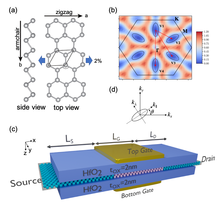
For the purpose of electronic transport simulation, the conduction band of arsenene and antimonene [a single-layer of arsenic/antimony atoms forming a buckled hexagonal honeycomb structure, see Fig. 1(a)] can be described as six energetically degenerate valleys, located at the midpoint of the -M line. We note that the next low-energy conduction band valley is 0.23 eV (0.27 eV) above the conduction band minimum for antimonene (arsenene), thus playing negligible roles in the electronic transport at 300 K. In our simulations, we restrict ourselves to consider the six low-lying valleys, modeled within an anisotropic effective-mass approximation, as described in Sec. IV.1. We have verified that this is enough to include the relevant states for transport at the doping level and temperature (300 K) considered in this work. In this regard, we compare in Fig. 2 the transfer characteristics computed in the ballistic regime within our model for an antimonene-based MOSFET with the corresponding data obtained by using an atomistic full-band model in Ref. Pizzi et al., 2016. The good agreement between our results (dashed line) and those obtained within the atomistic full-band model (dots) confirms the validity and accuracy of our approach. The spin-orbit coupling is neglected in this work since it does not affect appreciably the conduction band, as also shown in Ref. Pizzi et al., 2016.
| antimonene | arsenene | |||||
| 0.51 | 0.46 | |||||
| 0.15 | 0.15 | |||||
| [eV/Å2] | 1.948† | 3.271† | ||||
| Intravalley EPC | ||||||
| [eV/cm] | 8.07 | 1.09 | ||||
| [eV/cm] | 4.90 | 7.03 | ||||
| [meV] | 20 | 27 | ||||
| [meV] | 16 | 23 | ||||
| [eV] | 3.265† | 3.815† | ||||
| intervalley EPC | (V1V2) | (V1V3) | (V1V4) | (V1V2) | (V1V3) | (V1V4) |
| [ eV/cm] | 3.55 | 9.37 | 2.22 | 4.78 | 7.37 | 1.74 |
| [meV] | 3.50 | 8.89 | 7.26 | 5.81 | 8.89 | 7.26 |
| [ eV/cm] | 8.51 | 2.71 | 1.26 | 1.65 | 2.16 | 1.06 |
| [meV] | 4.76 | 8.97 | 8.53 | 7.97 | 8.97 | 8.53 |
| [ eV/cm] | 2.841 | 1.501 | 1.05 | 3.97 | 1.18 | 8.24 |
| [meV] | 6.58 | 13.90 | 10.07 | 9.58 | 13.89 | 10.07 |
| [ eV/cm] | 4.201 | 2.871 | 9.6 | 9.50 | 2.26 | 7.53 |
| [meV] | 17.0 | 24.08 | 24.81 | 24.61 | 24.08 | 24.81 |
| [ eV/cm] | 1.481 | 1.961 | 1.39 | 1.72 | 1.54 | 1.09 |
| [meV] | 17.8 | 27.17 | 26.19 | 25.85 | 27.17 | 26.19 |
| [ eV/cm] | 1.031 | 2.201 | 9.08 | 1.57 | 1.72 | 7.12 |
| [meV] | 20.7 | 27.58 | 30.59 | 30.26 | 27.58 | 30.59 |
II.2 Electron-phonon couplings from first-principles
We compute the relevant electron-phonon couplings from first-principles by using the density functional perturbation theory (DFPT). The values of the deformation potentials and phonon mode frequencies of intravalley and intervalley EPCs are listed in Table 1. The details about the DFPT calculations can be found in Sec. IV.3. As shown in Fig. 1(b), three types of intervalley EPCs connecting two electronic states located in different valleys (V1V2, V1V3, and V1V4) are considered. In the transport calculations, all the intravalley EPCs are included, while only the intervalley EPCs with a significant deformation potential ( eV/cm) are taken into account. Ignoring the smaller EPCs has very little effect on the results, since the electron-phonon self-energies depend quadratically on the deformation potential (see Eq. (6) in Sec. IV.2). The intravalley electron-ZA phonon interactions (not included in Table I) are neglected in our simulations. The validity of this approximation can be checked from Table S I and S II in the Supplementary Information, that report the scattering rates at the conduction band minima associated to each phonon mode. The data show that the intravalley scattering rates between electrons and ZA phonons are extremely small compared to all other scattering processes. Recently, it has been shown that in antimonene the electron-transverse acoustic (TA) phonon couplings are forbidden by symmetry for both intra- and intervalley scattering Wu et al. (2021), in good agreement with our numerical calculation here.
From Table 1, we can notice that some intervalley EPCs have deformation potential values almost an order of magnitude larger than those of the intravalley EPCs. Due to the relatively low phonon frequencies in antimonene and arsenene, those phonon modes can be thermally populated at room temperature, which leads to increased scattering of electrons through both emission and absorption of phonons. Therefore, the intervalley EPCs are expected to play a non-negligible role in the electronic transport and sensibly affect the MOSFET performance. This is confirmed by our quantum transport simulations, presented in the next section.
II.3 Quantum transport simulations with dissipation
Our aim is to provide quantitative and precise predictions of the optimum performance of these devices, when all the extrinsic sources of scattering are eliminated. Under these hypotheses, the electron-phonon interaction represents the dominant scattering mechanism at room temperature.
Based on the electronic model and the EPC models presented in the previous sections, we have built a dissipative quantum transport solver including all the elastic and inelastic electron-phonon scattering mechanisms, while still keeping the computational burden at the minimum level. More details on the quantum transport model are given in Sec. IV.2.
We focus on -type MOSFET devices. A sketch of the simulated device structure is drawn in Fig. 1(c). We consider a double-gate MOSFET architecture with source and drain extensions chemically doped at a donor concentration cm-2 and gate lengths ranging from 4 to 9 nm. The channel is undoped and has the same length of the gates. The effective oxide thickness is chosen to be 0.42 nm (corresponding to a 2 nm thick HfO2 high- dielectric layer), and the supply voltage is =0.55 V, according to the ITRS specifications itr .
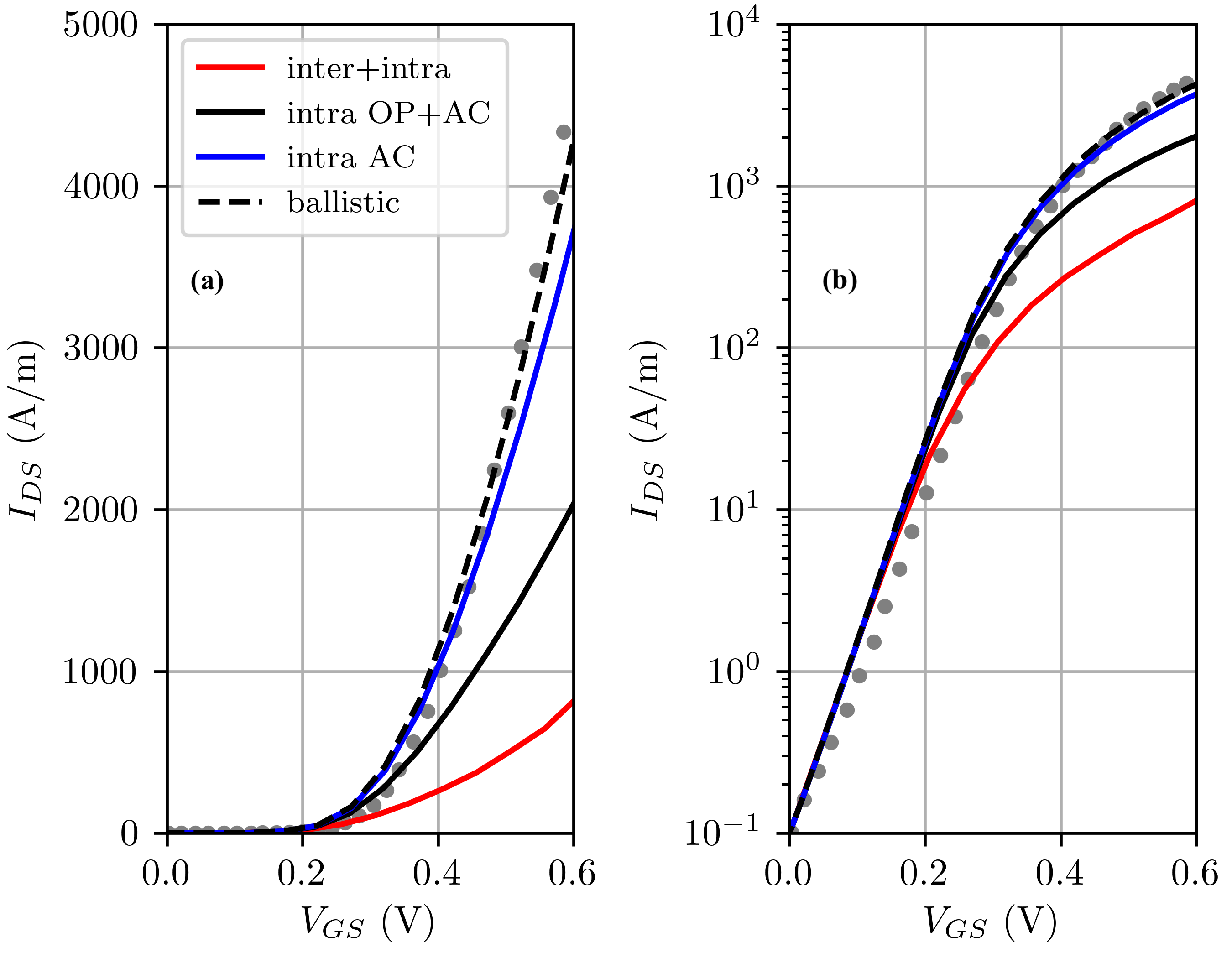
We show in Fig. 2 the transfer characteristics of armchair-antimonene-based MOSFET with nm. To illustrate the role played by the different electron-phonon scattering channels we carry out the simulations in three cases: (1) including only the intravalley acoustic scattering (elastic), (2) including only the intravalley scattering (elastic and inelastic), and (3) including all the intravalley and intervalley scattering (elastic and inelastic).
For a clearer comparison of different calculations and following the common practice, we shift all the transfer characteristics in order to set the OFF state, chosen to be the device state in which A/m itr , at . Accordingly, the ON state is at =0.55 V, and the corresponding current defines the ON current (). The subthreshold swing (SS) is defined as the inverse slope of the - curve in semi-logarithmic scale in the subthreshold regime ( A/m), SS=.
As shown in Fig. 2 for an antimonene-based MOSFET with nm, the SS is unaffected by the EPC. However, the ON state performance is strongly degraded, especially by the intervalley scatterings, consistently with the high amplitude of the associated deformation potentials. In quantitative terms, when all the significant scattering processes are included, the ON current drops by a factor larger than 4 with respect to the ballistic or ADP scattering approximation. Similar results are obtained in the case of the MOSFET based on arsenene and can be found in the Supplementary Information. More in general, these data strongly suggest that modeling the transport in 2D-material-based transistors as elastic, either in the ballistic or in the ADP scattering approximation, is not sufficient to reliably predict the device performance. On the contrary, inelastic intravalley and intervalley scattering mechanisms dominate and significantly affect the transport, even at gate lengths as short as 5 nm.
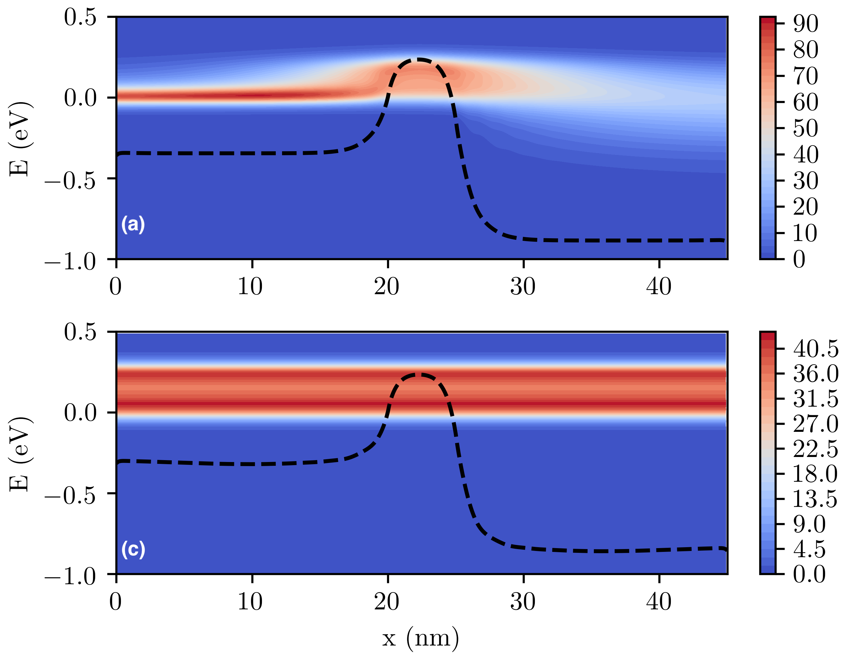
To elucidate the effects of EPC on the charge transport all along the device, we plot in Fig. 3 the current spectrum in the OFF and in the ON states for 5 nm. We consider both the case in which all the relevant scattering processes are included (panels (a) and (b)) and the case in which only the elastic scattering between electrons and acoustic phonons is taken into account (panels (c) and (d)). We first compare the current spectra in the OFF state. In Fig. 3 (a), it can be seen that the injection energies associated to the inelastic current spectrum gather around the source Fermi level (set to 0 eV). However, close to the barrier the spectrum broadens over a wider energy window, similar to that over which the elastic current concentrates (Fig. 3 (c)). This effect is driven by the significant optical phonon absorption, which rises electrons at energies for which the tunneling probability through the barrier is higher. The net result is that the barycenter of the inelastic current spectrum crossing the barrier is close to that observed in elastic transport conditions. Moreover, due to the smallness of the charge density in the channel in the subthreshold region, the conduction band profile is unaffected by the transport and only determined by the device geometry and by the dielectric properties of the materials (see the Supplementary Information for related data). Particularly, the efficiency of the gate in modulating the barrier turns out to be independent of the electron-phonon scattering processes taken into account. Since the SS is completely determined by the energy distribution of carriers and by the gate modulation efficiency, the previous considerations explain the closeness between the SS values in the elastic and inelastic transport cases. This argument holds respectless of the considered gate length (see the Supplementary Information for the data at =9 nm).
We now focus on the ON state. The current spectrum in Fig. 3 (b) and (d), shows that, contrarily to the behavior in the OFF state, electrons are now mainly injected at higher energies with respect to the top of the channel barrier. The current spectrum in Fig. 3 (b), obtained by including the inelastic scattering processes, demonstrates that electrons gradually lose energy by emitting optical phonons. The strong emission processes entail a significant backscattering and explains the considerable decrease of the current with respect to the case in which only elastic electron-phonon interactions are considered.

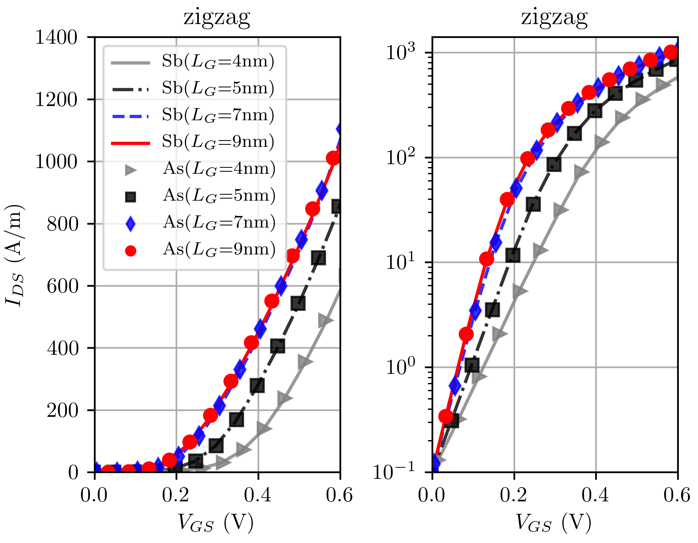
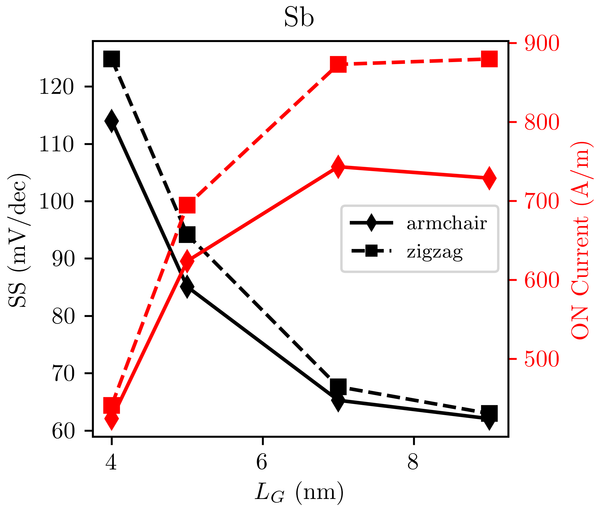
Figure 4 summarizes the simulated transfer characteristics of the antimonene- and arsenene-based MOSFET for varying from 4 to 9 nm, and the transport axis along the armchair and zigzag directions. All the relevant electron-phonon scattering processes are included. In all the considered cases the antimonene- and arsenene-based devices exhibit very similar transfer characteristics. The extracted SS and the ON current for the antimonene-based MOSFET are reported in Fig. 5. The very similar data obtained for the arsenene-based transistor can be found in the Supplementary Information. We observe that the armchair and zigzag transport directions are not equivalent, since the rotation by /4 needed to switch between them is not a symmetry of the crystal. Particularly, while the density of states and the scattering rates associated to the six degenerate valleys are invariant under arbitrary rotations, the anisotropy of the valleys makes the average effective mass seen in the armchair and zigzag directions different. The higher ON current in the zigzag direction arises from a smaller average transport effective mass , and thus a higher group velocity. On the other hand, the smaller entails a larger source-to-drain tunneling (STDT), which results in higher SS values.
II.4 Reducing phonon scattering by valley-engineering
Since the six-fold degenerate conduction band valleys are inherited from the crystal rotational symmetry, applying an external symmetry-breaking uniaxial strain along the zigzag direction (see Fig. 1) can split the six valleys into four higher-energy and two lower-energy valleys on the armchair axis. On the contrary, if the uniaxial strain is along the armchair direction, only two valleys will be pushed up to higher energy Sohier et al. (2019). In the following, we will consider the uniaxial strain along the zigzag direction. A sizable splitting of 0.16 eV can be obtained for a small uniaxial strain of 2% in the case of arsenene, while the splitting is 0.1 eV in antimonene Sohier et al. (2019). The effect on EPC and effective masses by such small strain has been shown to be negligible Sohier et al. (2019). Instead, since the strain shifts the energy of the valleys, it effectively turns off the intervalley scattering channels between the lower-energy and the higher-energy valleys. In addition, the transport becomes anisotropic, since the two lower-lying valleys both have the large effective mass in the armchair direction and the small one in the zigzag direction.
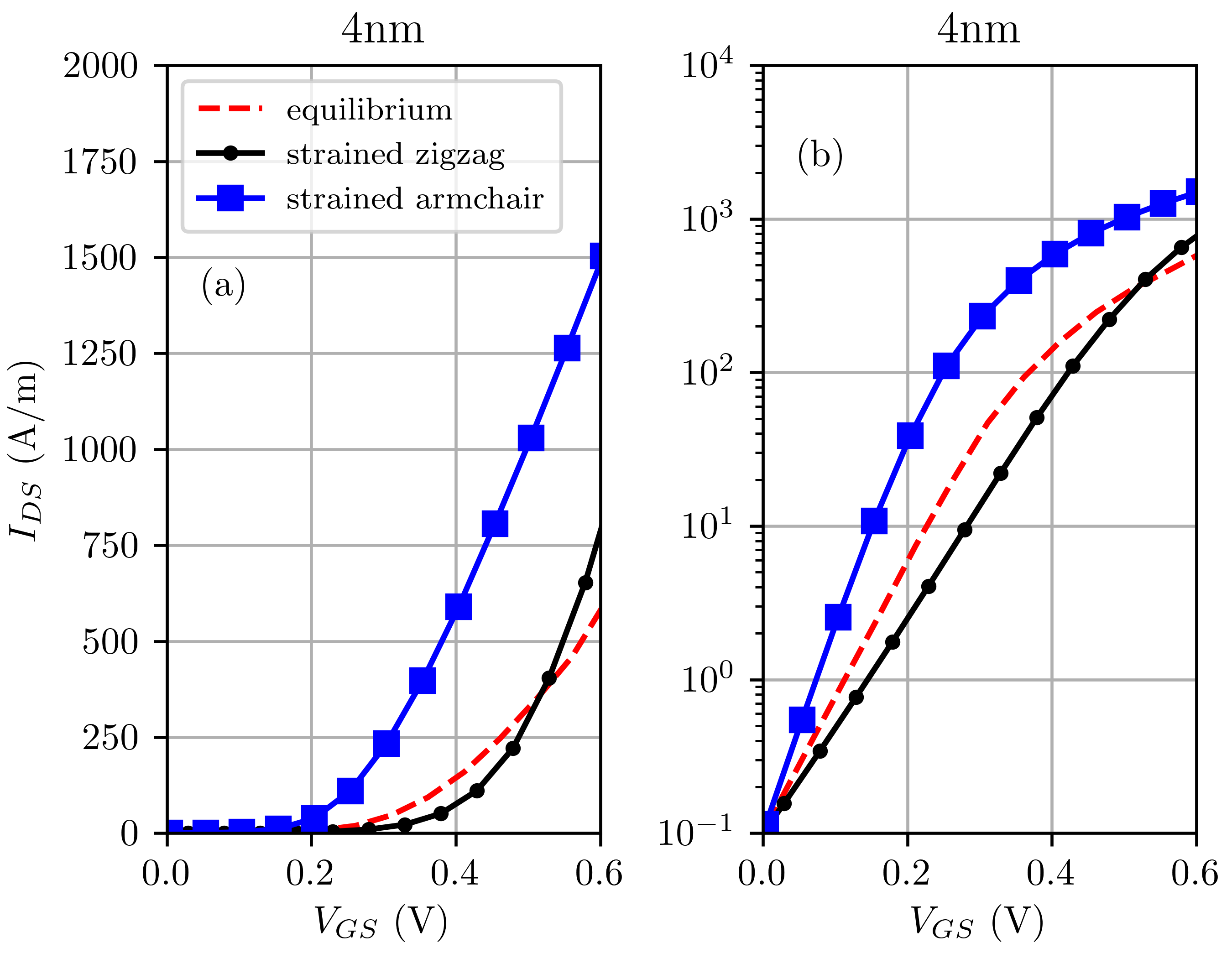
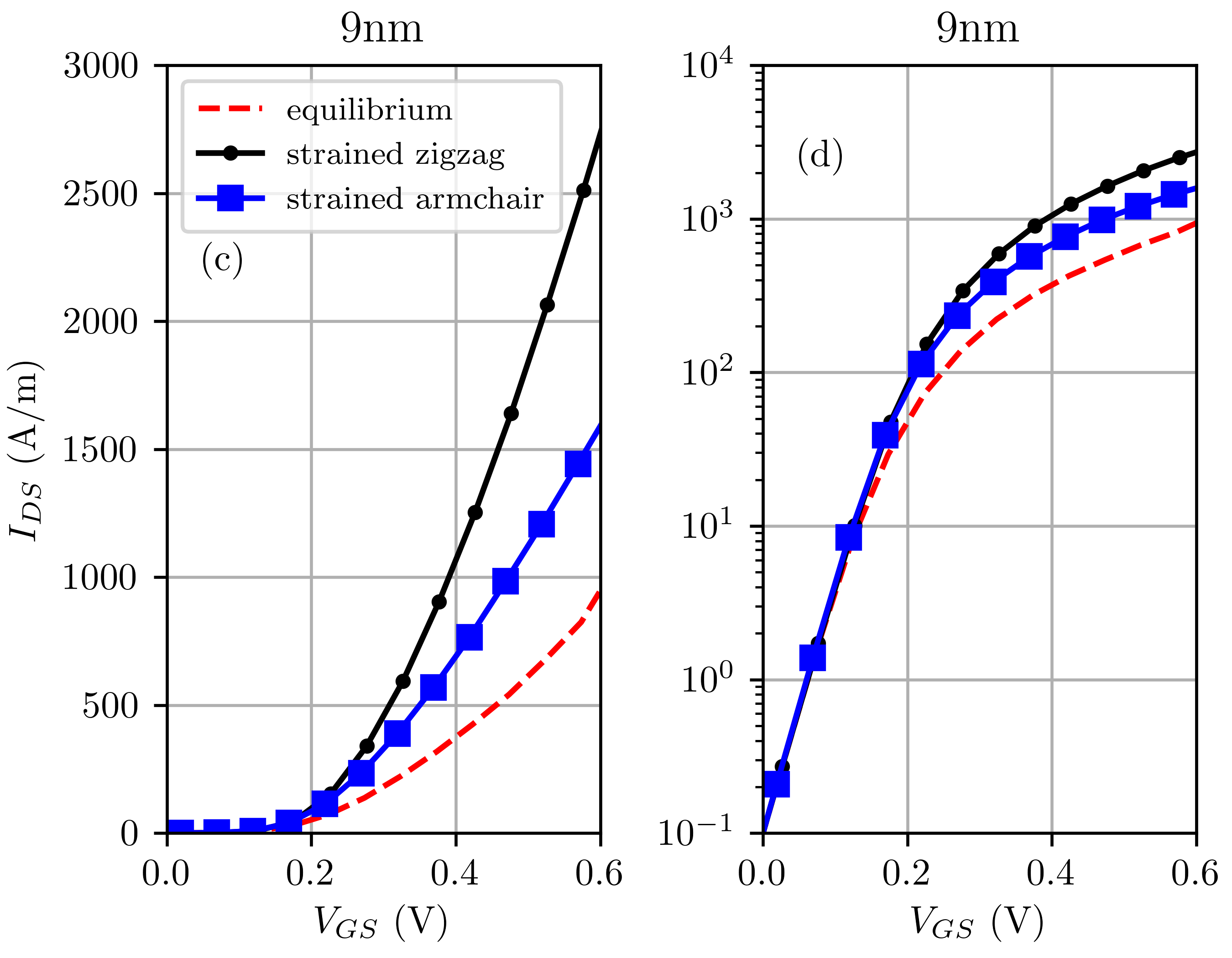
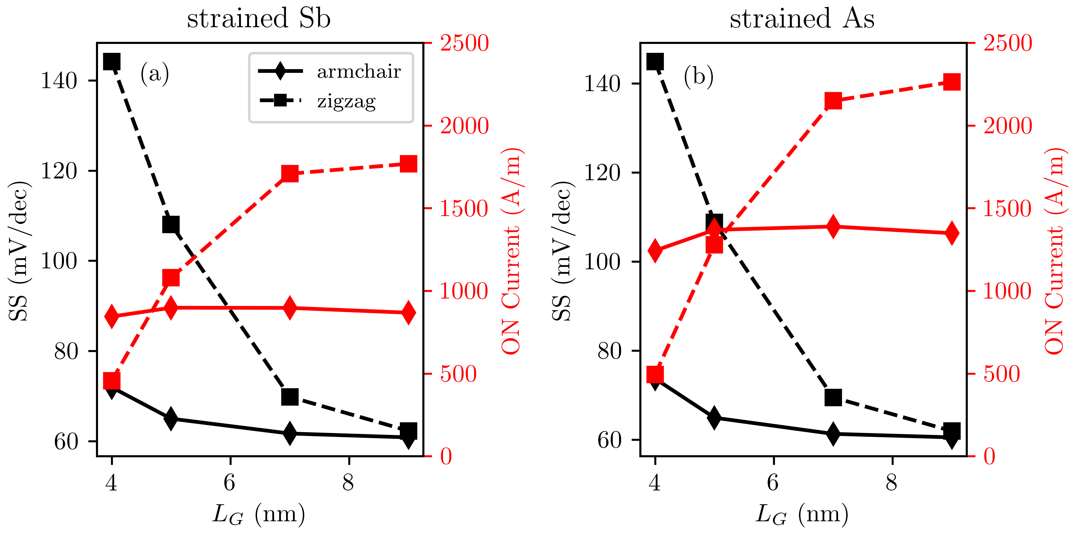
Figure 6 compares the transfer characteristics of the strained-arsenene-based MOSFET along the armchair and zigzag directions, for =4 and 9 nm. The transfer characteristics of the unstrained device are also plotted for reference. The simulations clearly shows an improvement of the ON current for all the considered configurations. Such an improvement is in excess of a factor 2.5 in the zigzag direction for =9 nm and amounts to approximately a factor 2 in the armchair direction for =4 nm. Similar improvements (a factor of 2.4 in the zigzag direction for =9 nm and 2 in the armchair direction for =4 nm) are obtained for MOSFETs based on strained antimonene. The corresponding data are reported in the Supplementary Information.
The SS and for both arsenene- and antimonene-based MOSFETs are quantified in Fig. 7 for =4, 5, 7, and 9 nm. The plots shows that, while the transistors fabricated by using the two monolayers exhibit almost identical SSs as a function of , that based on arsenene can achieve higher values of . In both cases, at short channel lengths (< 5 nm) the best performance are obtained when the transport occurs along the armchair direction. Indeed, due to the higher effective mass along this direction, the is less degraded by the STDT, which results in a better scaling behavior. On the contrary, at longer gate lengths, the transport along the zigzag direction is more advantageous, due to the higher injection velocity associated to the small effective mass. We remark that also the low ratio plays a significant role in enhancing the carrier velocity, since at each given energy it entails a larger kinetic component in the transport direction.
III Conclusion
We have investigated the dissipative transport in single-layer arsenene and antimonene MOSFETs by performing first-principle-based NEGF quantum simulations including all the relevant intra- and intervalley electron-phonon scattering mechanisms. We have shown that even for a gate length of 5 nm the ON current can be strongly decreased by the optical intravalley and intervalley phonon scatterings, and that, as a consequence, the simulations in the ballistic regime and/or only including the acoustic phonon scattering can largely overestimate the performance of real devices. Due to the combination of the six-fold degeneracy of the conduction band valleys, the large magnitude of the electron-phonon couplings, and the low optical phonon frequencies, the intervalley electron-phonon scattering is the dominant scattering mechanism in the arsenene- and antimonene-based MOSFETs at room temperature.
Moreover, we have investigated a viable approach to mitigate the impact of intervalley phonon scattering by removing the valley degeneracy via a small uniaxial strain along the zigzag direction. Our calculations indicate that for gate lengths larger than 5 nm, the ON current in the zigzag direction can be increased by a factor 2.5. For gate lengths shorter than 5 nm, selecting the armchair direction as the transport direction minimizes the source-to-drain tunneling effect and results in a two times ON-current improvement with respect to the case with unstrained material.
Overall, our work can provide useful guidelines to the simulation of transistors based on 2D materials, and suggests that there are room and opportunities to overcome the obstacles on the way towards the development of a future 2D-based electronics.
IV Methods
IV.1 The anisotropic effective mass model
The conduction band of Sb and As monolayers has six-fold degenerate valleys located at the midpoint of the -M paths. These valleys have a larger effective mass along the high-symmetry -M direction, denoted by . The effective mass along the direction perpendicular to -M is denoted by . By using local -coordinates for each valley, we can write the conduction band energy in the anisotropic effective mass model as
| (1) |
where is the reduced Planck constant, the electron mass, and , the wavevector components along the -M and the orthogonal direction, respectively. For transport calculations, we need to express and in terms of and , namely the wave vector components in the transport and transverse directions, respectively (see Fig. 1 (d)):
| (2) |
where denotes the angle between the -axis and the transport direction .
The kinetic energy of electrons in terms of and reads:
| (3) |
The Hamiltonian in the form employed in the simulations is obtained by replacing with the differential operator . We enforce periodic boundary conditions in the transverse direction, thus the Hamiltonian maintains a parametric dependence on . The value of to be considered for each valley depends on the chosen transport direction (armchair or zigzag).
IV.2 Quantum transport
To simulate the electron transport, we adopt the Keldysh-Green’s function formalism Fetter and Walecka (2003), which allows us to include the electron-phonon coupling by means of local self-energies. We self-consistently solve the following equations for every valley
| (4) |
where is the electron energy, is the identity matrix, is the anisotropic effective mass Hamiltonian matrix, and are the retarded self-energies corresponding to source and drain contacts and to the electron-phonon coupling, is the retarded Green’s function, and , and are the corresponding lesser-than and greater-than quantities. Equations (4) are spatially discretized over a uniform mesh with stepsize equal to 0.5 Å.
For the intravalley acoustic phonons, the local self-energies at the -th discrete space site along the transport direction at room temperature can be expressed in the quasi-elastic approximation as Rogdakis et al. (2009)
| (5) |
where is the elastic modulus, the acoustic deformation potential, the Boltzmann constant, the temperature, the transverse phonon wavevector and is the valley index.
For the intravalley optical phonons, the self-energies related to a phonon with branch can be expressed as
| (6) |
where is the mass density, is the Bose-Einstein distribution at temperature of a phonon with frequency at point, and the upper/lower sign of the term corresponds to lesser/greater-than self-energies.
The self-energies associated to the intervalley scattering are analogously obtained as:
| (7) |
where is the phonon wavevectors connecting two degenerate valley minima, and the three scattering processes shown in Fig. 1 are considered.
The total lesser-than and greater-than self-energies are obtained by summing the self-energies associated to all the different scattering processes. The retarded self-energy is then computed by
| (8) |
The real part of the retarded self-energy, which only contributes to a shift of the energy levels, is neglected.
Equations (4-8) are iteratively solved within the so-called self-consistent Born approximation (SCBA) until the convergence is achieved. The SCBA convergence ensures that the electronic current is conserved along the device structure. Once the SCBA loop achieves the convergence, the electron and transport current densities are determined from the Green’s functions of all the valleys
| (9) |
and
| (10) |
where the integration range from to includes all the energy states contributing to transport. We discretize the energy into a uniform grid with a stepsize meV for antimonene and meV for arsenene. Each energy interval of width is further discretized by defining 3 quadrature nodes. The charge and current densities are computed by first performing an integration over each interval by using the Gauss-Legendre quadrature rule and then adding the contributions of all the intervals. The 2D charge density is used to set up the Poisson equation, which is solved in the device - cross-section. The simulation runs over a loop between the Green’s function equations and the Poisson problem until an overall self-consistent solution is reached.
IV.3 First-principles calculation details
The DFT simulations were performed in a plane wave basis by means of the Quantum Espresso suite Giannozzi et al. (2009, 2017). The antimonene and arsenene monolayers were simulated by using scalar relativistic norm-conserving pseudopotentials based on the local density approximation exchange-correlation functional. In both cases, a Monkhorst-Pack (M-P) k-point grid was used, with a cutoff energy of 90 Ry. A vacuum layer of 28 Å is considered along the perpendicular direction to eliminate the interlayer interactions due to the periodic boundary conditions.
The phonon dispersion relations were computed within the DFPT framework by using a 881 M-P -point grid and a 16161 M-P -point grid.
The electron-phonon matrix elements between two electronic states and connected by a phonon mode of wavevector were computed within the DFTP framework as
| (11) |
where is the unit cell mass, and are band indices, and is the lattice periodic part of the perturbed Kohn-Sham potential expanded to first order in the atomic displacement. The were computed on a 16161 -point grid and a 881 -point grid, and then interpolated on a denser grid by projection on a basis of maximally localized Wannier functions by using the wannier90 code Pizzi et al. (2020) and the EPW code Poncé et al. (2016). Six Wannier orbitals were employed to reproduce accurately the conduction and valence bands close to the bandgap and achieve good spatial localization of the Wannier orbitals. The scattering rates for each phonon mode were computed through the EPW code, by interpolating the electron-phonon matrix elements on a 1201201 -point grid. The intravalley and intervalley electron-phonon coupling were described by the matrix element at and , respectively, where and correspond to two degenerate valley minima. The deformation potentials were finally computed as
| (12) |
V Data Availability
The data that support the findings of this study are available from the corresponding author upon reasonable request.
Supporting Information
Acknowledgements
This work is supported by Natural Science Foundation of Jiangsu Province under Grants No. BK20180456 and BK20180071, and National Natural Science Foundation of China under Grant No. 11374063. M.P. acknowledges financial support from the Agence Nationale de la Recherche through the "2D-ON-DEMAND" project (Grant No. ANR-20-CE09-0026-02). J.C. acknowledges support from the European Unions Horizon 2020 Research and Innovation Programme, under the Marie Skłodowska-Curie Grant Agreement "CAMPVANS" No. 885893. S.Z. acknowledges financial support from the Training Program of the Major Research Plan of the National Natural Science Foundation of China (Grant No. 91964103). H.Z. acknowledges financial support from the Shanghai Municipal Natural Science Foundation under Grant No. 19ZR1402900.
Author Contribution
J.C., D.L. and M.P. developed the theory and simulation code for the quantum transport calculations. J.C. performed the quantum transport simulations and analysed the data. Y.W. and H.Z. performed the ab-initio calculations. M.P., H.Z. and S.Z. designed the simulations. All the authors discussed the results and contributed to the writing of the manuscript.
Competing Interests
The authors declare that there are no competing interests.
References
- Fiori et al. (2014) G. Fiori, F. Bonaccorso, G. Iannaccone, T. Palacios, D. Neumaier, A. Seabaugh, S. K. Banerjee, and L. Colombo, “Electronics based on two-dimensional materials,” Nat. Nanotechnol. 9, 768–779 (2014).
- Novoselov et al. (2016) K. S. Novoselov, A. Mishchenko, A. Carvalho, and A. H. Castro Neto, “2D materials and van der Waals heterostructures,” Science 353 (2016).
- Schaibley et al. (2016) J. R. Schaibley, H. Yu, G. Clark, P. Rivera, J. S. Ross, K. L. Seyler, W. Yao, and X. Xu, “Valleytronics in 2D materials,” Nat. Rev. Mater. 1, 16055 (2016).
- Yang, Jiang, and Wei (2017) S. Yang, C. Jiang, and S.-h. Wei, “Gas sensing in 2D materials,” Appl. Phys. Rev. 4, 021304 (2017).
- Jin et al. (2018) C. Jin, E. Y. Ma, O. Karni, E. C. Regan, F. Wang, and T. F. Heinz, “Ultrafast dynamics in van der Waals heterostructures,” Nat. Nanotechnol. 13, 994–1003 (2018).
- Liu and Hersam (2019) X. Liu and M. C. Hersam, “2D materials for quantum information science,” Nat. Rev. Mater. 4, 669–684 (2019).
- Das et al. (2019) S. Das, D. Pandey, J. Thomas, and T. Roy, “The Role of Graphene and Other 2D Materials in Solar Photovoltaics,” Adv. Mater. 31, 1802722 (2019).
- Zhang et al. (2018) S. Zhang, S. Guo, Z. Chen, Y. Wang, H. Gao, J. Gómez-Herrero, P. Ares, F. Zamora, Z. Zhu, and H. Zeng, “Recent progress in 2D group-VA semiconductors: from theory to experiment,” Chem. Soc. Rev. 47, 982–1021 (2018).
- Radisavljevic et al. (2011) B. Radisavljevic, A. Radenovic, J. Brivio, V. Giacometti, and A. Kis, “Single-layer MoS2 transistors,” Nat. Nanotechnol. 6, 147–150 (2011).
- Wang et al. (2012) H. Wang, L. Yu, Y.-H. Lee, Y. Shi, A. Hsu, M. L. Chin, L.-J. Li, M. Dubey, J. Kong, and T. Palacios, “Integrated Circuits Based on Bilayer MoS2 Transistors,” Nano Lett. 12, 4674–4680 (2012).
- Chhowalla, Jena, and Zhang (2016) M. Chhowalla, D. Jena, and H. Zhang, “Two-dimensional semiconductors for transistors,” Nat. Rev. Mater. 1, 16052 (2016).
- Cao et al. (2016) J. Cao, D. Logoteta, S. Özkaya, B. Biel, A. Cresti, M. G. Pala, and D. Esseni, “Operation and Design of van der Waals Tunnel Transistors: A 3-D Quantum Transport Study,” IEEE Trans. Electron Devices 63, 4388–4394 (2016).
- Pizzi et al. (2016) G. Pizzi, M. Gibertini, E. Dib, N. Marzari, G. Iannaccone, and G. Fiori, “Performance of arsenene and antimonene double-gate MOSFETs from first principles,” Nat. Commun. 7, 12585 (2016).
- Polyushkin et al. (2020) D. K. Polyushkin, S. Wachter, L. Mennel, M. Paur, M. Paliy, G. Iannaccone, G. Fiori, D. Neumaier, B. Canto, and T. Mueller, “Analogue two-dimensional semiconductor electronics,” Nat. Electron. 3, 486–491 (2020).
- Allain et al. (2015) A. Allain, J. Kang, K. Banerjee, and A. Kis, “Electrical contacts to two-dimensional semiconductors,” Nat. mater. 14, 1195–1205 (2015).
- Allain and Kis (2014) A. Allain and A. Kis, “Electron and Hole Mobilities in Single-Layer WSe2,” ACS Nano 8, 7180–7185 (2014).
- Li et al. (2014) L. Li, Y. Yu, G. J. Ye, Q. Ge, X. Ou, H. Wu, D. Feng, X. H. Chen, and Y. Zhang, “Black phosphorus field-effect transistors,” Nat. Nanotechnol. 9, 372–377 (2014).
- Liu et al. (2018) Y. Liu, X. Duan, Y. Huang, and X. Duan, “Two-dimensional transistors beyond graphene and tmdcs,” Chem. Soc. Rev. 47, 6388–6409 (2018).
- Sohier et al. (2018) T. Sohier, D. Campi, N. Marzari, and M. Gibertini, “Mobility of two-dimensional materials from first principles in an accurate and automated framework,” Phys. Rev. Materials 2, 114010 (2018).
- Cheng, Zhang, and Liu (2020) L. Cheng, C. Zhang, and Y. Liu, “Why Two-Dimensional Semiconductors Generally Have Low Electron Mobility,” Phys. Rev. Lett. 125, 177701 (2020).
- Poncé, Margine, and Giustino (2018) S. Poncé, E. R. Margine, and F. Giustino, “Towards predictive many-body calculations of phonon-limited carrier mobilities in semiconductors,” Phys. Rev. B 97, 121201 (2018).
- Poli et al. (2008) S. Poli, M. G. Pala, T. Poiroux, S. Deleonibus, and G. Baccarani, “Size Dependence of Surface-Roughness-Limited Mobility in Silicon-Nanowire FETs,” IEEE Trans. Electron Devices 55, 2968–2976 (2008).
- Grillet et al. (2017) C. Grillet, D. Logoteta, A. Cresti, and M. G. Pala, “Assessment of the Electrical Performance of Short Channel InAs and Strained Si Nanowire FETs,” IEEE Trans. Electron Devices 64, 2425–2431 (2017).
- Liao et al. (2020) W. Liao, S. Zhao, F. Li, C. Wang, Y. Ge, H. Wang, S. Wang, and H. Zhang, “Interface engineering of two-dimensional transition metal dichalcogenides towards next-generation electronic devices: recent advances and challenges,” Nanoscale Horiz. 5, 787–807 (2020).
- Kaasbjerg, Thygesen, and Jacobsen (2012) K. Kaasbjerg, K. S. Thygesen, and K. W. Jacobsen, “Phonon-limited mobility in -type single-layer MoS2 from first principles,” Phys. Rev. B 85, 115317 (2012).
- Fischetti and Vandenberghe (2016) M. V. Fischetti and W. G. Vandenberghe, “Mermin-Wagner theorem, flexural modes, and degraded carrier mobility in two-dimensional crystals with broken horizontal mirror symmetry,” Phys. Rev. B 93, 155413 (2016).
- Sohier, Calandra, and Mauri (2016) T. Sohier, M. Calandra, and F. Mauri, “Two-dimensional Fröhlich interaction in transition-metal dichalcogenide monolayers: Theoretical modeling and first-principles calculations,” Phys. Rev. B 94, 085415 (2016).
- Cheng and Liu (2018) L. Cheng and Y. Liu, “What limits the intrinsic mobility of electrons and holes in two dimensional metal dichalcogenides?” Journal of the American Chemical Society, Journal of the American Chemical Society 140, 17895–17900 (2018).
- Cheng, Zhang, and Liu (2019) L. Cheng, C. Zhang, and Y. Liu, “The optimal electronic structure for high-mobility 2d semiconductors: Exceptionally high hole mobility in 2d antimony,” Journal of the American Chemical Society, Journal of the American Chemical Society 141, 16296–16302 (2019).
- Szabó, Rhyner, and Luisier (2015) A. Szabó, R. Rhyner, and M. Luisier, “Ab initio simulation of single- and few-layer transistors: Effect of electron-phonon scattering,” Phys. Rev. B 92, 035435 (2015).
- Logoteta et al. (2020) D. Logoteta, J. Cao, M. Pala, P. Dollfus, Y. Lee, and G. Iannaccone, “Cold-source paradigm for steep-slope transistors based on van der Waals heterojunctions,” Phys. Rev. Research 2, 043286 (2020).
- Takagi et al. (1994) S. Takagi, A. Toriumi, M. Iwase, and H. Tango, “On the universality of inversion layer mobility in Si MOSFET’s: Part I-effects of substrate impurity concentration,” IEEE Trans. Electron Devices 41, 2357–2362 (1994).
- Bardeen and Shockley (1950) J. Bardeen and W. Shockley, “Deformation Potentials and Mobilities in Non-Polar Crystals,” Phys. Rev. 80, 72–80 (1950).
- Wang et al. (2017) Y. Wang, P. Huang, M. Ye, R. Quhe, Y. Pan, H. Zhang, H. Zhong, J. Shi, and J. Lu, “Many-body Effect, Carrier Mobility, and Device Performance of Hexagonal Arsenene and Antimonene,” Chem. Mater. 29, 2191–2201 (2017).
- Sohier et al. (2019) T. Sohier, M. Gibertini, D. Campi, G. Pizzi, and N. Marzari, “Valley-Engineering Mobilities in Two-Dimensional Materials,” Nano Lett. 19, 3723–3729 (2019).
- Pala et al. (2016) M. G. Pala, C. Grillet, J. Cao, D. Logoteta, A. Cresti, and D. Esseni, “Impact of inelastic phonon scattering in the off state of tunnel-field-effect transistors,” J. Comput. Electron. 15, 1240–1247 (2016).
- Klinkert et al. (2020) C. Klinkert, Á. Szabó, C. Stieger, D. Campi, N. Marzari, and M. Luisier, “2-D Materials for Ultrascaled Field-Effect Transistors: One Hundred Candidates under the Ab Initio Microscope,” ACS Nano 14, 8605–8615 (2020).
- Wu et al. (2021) Y. Wu, B. Hou, C. Ma, J. Cao, Y. Chen, Z. Lu, H. Mei, H. Shao, Y. Xu, H. Zhu, Z. Fang, R. Zhang, and H. Zhang, “Thermoelectric performance of 2d materials: the band-convergence strategy and strong intervalley scatterings,” Mater. Horiz. , Advance Article (2021).
- (39) “See “International Technology Roadmap for Semiconductors” (last accessed November 25, 2020),” .
- Fetter and Walecka (2003) A. Fetter and J. Walecka, Quantum Theory of Many-Particle Systems (Dover, New York, 2003).
- Rogdakis et al. (2009) K. Rogdakis, S. Poli, E. Bano, K. Zekentes, and M. G. Pala, “Phonon- and surface-roughness-limited mobility of gate-all-around 3C-SiC and Si nanowire FETs,” Nanotechnology 20, 295202 (2009).
- Giannozzi et al. (2009) P. Giannozzi, S. Baroni, N. Bonini, M. Calandra, R. Car, C. Cavazzoni, D. Ceresoli, G. L. Chiarotti, M. Cococcioni, I. Dabo, A. Dal Corso, S. de Gironcoli, S. Fabris, G. Fratesi, R. Gebauer, U. Gerstmann, C. Gougoussis, A. Kokalj, M. Lazzeri, L. Martin-Samos, N. Marzari, F. Mauri, R. Mazzarello, S. Paolini, A. Pasquarello, L. Paulatto, C. Sbraccia, S. Scandolo, G. Sclauzero, A. P. Seitsonen, A. Smogunov, P. Umari, and R. M. Wentzcovitch, “QUANTUM ESPRESSO: a modular and open-source software project for quantum simulations of materials,” J. Phys.: Condensed Matter 21, 395502 (19pp) (2009).
- Giannozzi et al. (2017) P. Giannozzi, O. Andreussi, T. Brumme, O. Bunau, M. B. Nardelli, M. Calandra, R. Car, C. Cavazzoni, D. Ceresoli, M. Cococcioni, N. Colonna, I. Carnimeo, A. D. Corso, S. de Gironcoli, P. Delugas, R. A. D. Jr, A. Ferretti, A. Floris, G. Fratesi, G. Fugallo, R. Gebauer, U. Gerstmann, F. Giustino, T. Gorni, J. Jia, M. Kawamura, H.-Y. Ko, A. Kokalj, E. Küçükbenli, M. Lazzeri, M. Marsili, N. Marzari, F. Mauri, N. L. Nguyen, H.-V. Nguyen, A. O. de-la Roza, L. Paulatto, S. Poncé, D. Rocca, R. Sabatini, B. Santra, M. Schlipf, A. P. Seitsonen, A. Smogunov, I. Timrov, T. Thonhauser, P. Umari, N. Vast, X. Wu, and S. Baroni, “Advanced capabilities for materials modelling with QUANTUM ESPRESSO,” J. Phys.: Condensed Matter 29, 465901 (2017).
- Pizzi et al. (2020) G. Pizzi, V. Vitale, R. Arita, S. Blügel, F. Freimuth, G. Géranton, M. Gibertini, D. Gresch, C. Johnson, T. Koretsune, J. Ibañez-Azpiroz, H. Lee, J.-M. Lihm, D. Marchand, A. Marrazzo, Y. Mokrousov, J. I. Mustafa, Y. Nohara, Y. Nomura, L. Paulatto, S. Poncé, T. Ponweiser, J. Qiao, F. Thöle, S. S. Tsirkin, M. Wierzbowska, N. Marzari, D. Vanderbilt, I. Souza, A. A. Mostofi, and J. R. Yates, “Wannier90 as a community code: new features and applications,” J. Phys.: Condensed Matter 32, 165902 (2020).
- Poncé et al. (2016) S. Poncé, E. Margine, C. Verdi, and F. Giustino, “Epw: Electron–phonon coupling, transport and superconducting properties using maximally localized wannier functions,” Comput. Phys. Commun. 209, 116 – 133 (2016).