Integrated multiplexed microwave readout of silicon quantum dots in a cryogenic CMOS chip
Solid-state quantum computers require classical electronics to control and readout individual qubits and to enable fast classical data processing Arute et al. (2019); Watson et al. (2018); Reilly (2015). Integrating both subsystems at deep cryogenic temperatures Charbon et al. (2016), where solid-state quantum processors operate best, may solve some major scaling challenges, such as system size and input/output (I/O) data management Reilly (2019). Spin qubits in silicon quantum dots (QDs) could be monolithically integrated with complementary metal-oxide-semiconductor (CMOS) electronics using very-large-scale integration (VLSI) and thus leveraging over wide manufacturing experience in the semiconductor industry Maurand et al. (2016). However, experimental demonstrations of integration using industrial CMOS at mK temperatures are still in their infancy.
Here we present a cryogenic integrated circuit (IC) fabricated using industrial CMOS technology that hosts three key ingredients of a silicon-based quantum processor: QD arrays (arranged here in a non-interacting 33 configuration), digital electronics to minimize control lines using row-column addressing and analog LC resonators for multiplexed readout, all operating at 50 mK. With the microwave resonators (6-8 GHz range), we show dispersive readout of the charge state of the QDs and perform combined time- and frequency-domain multiplexing, enabling scalable readout while reducing the overall chip footprint.
This modular architecture probes the limits towards the realization of a large-scale silicon quantum computer integrating quantum and classical electronics using industrial CMOS technology.
Quantum computing is poised to be an innovation driver of the decade, given its theoretically-demonstrated capability to solve certain computational problems more efficiently than classical computers Montanaro (2016). However, constructing the required quantum hardware is one of the greatest technological challenges for the scientific community. Single electron spins isolated in silicon QDs are one of the most promising solid-state systems to achieve that goal: recent demonstrations of long coherence times Veldhorst et al. (2014), high-fidelity spin readout Urdampilleta et al. (2019), and one- and two-qubit gates Yoneda et al. (2018); Huang et al. (2019); Zajac et al. (2018), fulfill the basic requirements to build a quantum computer approaching fault-tolerant thresholds Fowler et al. (2012). Until now, silicon QDs have been typically fabricated using custom processes Kawakami et al. (2014); Veldhorst et al. (2014), but recent results have revealed they can be manufactured at scale using industry-compatible Maurand et al. (2016) or even industry-standard processes Yang et al. (2020a); Bonen et al. (2019). This allows to leverage the integration capabilities of the semiconductor industry to scale up.
Researchers have already produced blueprints of large-scale quantum computers in silicon Veldhorst et al. (2017); Vandersypen et al. (2017); Li et al. (2018). The proposals share common concepts: MOS-based QD arrays to host the qubits, digital electronics for I/O data management and analog classical electronics for control and readout. Full system integration will bring the benefits of reduced footprint, ease of signal synchronization, reduced latency and minimized inter-chip wiring. However, the ultimate level of possible integration is still uncertain, given the reduced cooling power availability at mK temperatures for typical classical electronics. Exploring the limits of integration is hence paramount to realize any fully-fledged solid-state quantum processor Le Guevel et al. (2020); Opremcak et al. (2018).
For silicon, one approach has been to operate qubits at elevated temperatures (1.2 K) Yang et al. (2020b); Petit et al. (2020) to enable larger cooling power budgets for the classical electronics Xue et al. (2020), but so far this has come at the cost of reduced fidelity and/or coherence times. Alternatively, ICs that operate at mK temperatures have been produced for control Pauka et al. (2019), readout Hornibrook et al. (2014), signal multiplexing Pauka et al. (2020); Potočnik et al. (2020); Paquelet Wuetz et al. (2020), or single devices have been used for time-multiplexed readout Schaal et al. (2019), but these circuits have not been fully integrated with the quantum devices.
Here we present an IC fabricated using industrial 40-nm CMOS technology that enables scalable multiplexed microwave readout of a non-interacting array of silicon QDs, all operating at mK temperatures in the same monolithic chip. The QDs are hosted in the channel of minimum size transistors and placed in a 33 array. Individual QDs can be randomly addressed via digital transistors using a row-column architecture to minimize the number of inputs. The readout is performed using gate-based microwave reflectometry, a technique readily compatible with industrial CMOS technology West et al. (2019). For the first time, we combine time- and frequency-domain multiplexing in one demonstration to minimize circuit footprint, otherwise compromised by using one readout resonator per qubit, while preserving a degree of parallel readout, ideal for quantum error correction.
A fully-integrated DRAM-like readout matrix architecture
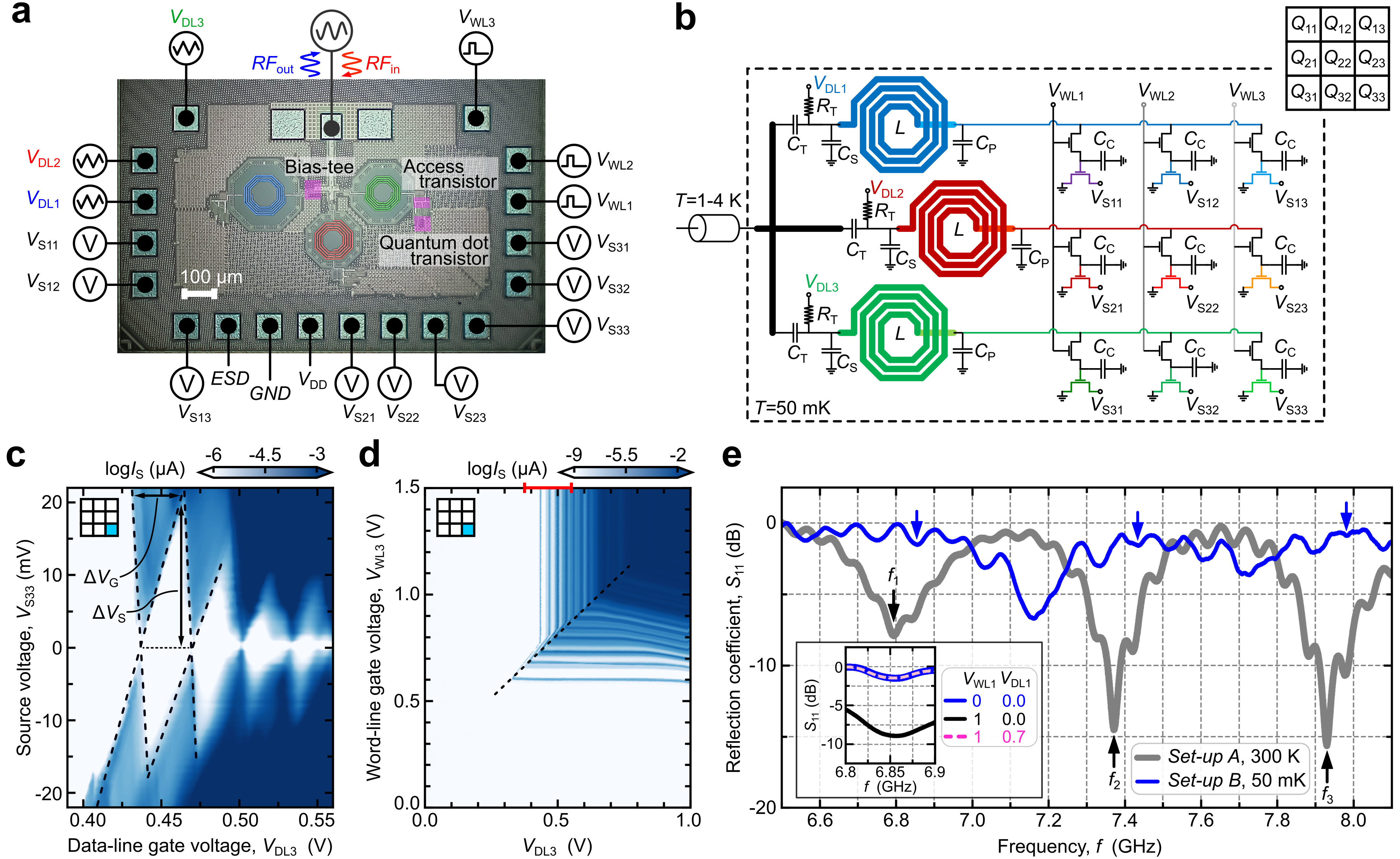
The proposed quantum-classical readout interface has been designed and fabricated in an industrial 40-nm bulk CMOS technology. Fig. 1a and Fig. 1b present the chip micrograph and its schematic, respectively. The modular architecture consists of a 33 array of 9 identical cells, arranged in a row-column random-access configuration similar to a dynamic random-access memory (DRAM). Each cell contains a silicon QD device, i.e. for =1,2,3, implemented as a MOS transistor. Furthermore, the gate of each quantum device is connected to the source of an access MOS transistor with a channel length =40 nm and a channel width =15 m, allowing conditional access, and to a storage capacitor (200 fF), to store the voltage at the gate of the quantum device (see Supplementary Information S1). The access transistors in column are controlled by the same word-line signal . The cells in row are connected to both a shared data-line signal , providing a bias voltage to control the QDs through an on-chip bias-tee, and a LC resonator , to perform microwave reflectometry readout Colless et al. (2013); Wallraff et al. (2004). When applying data-line voltage and word-line voltage , a quantum device is accessed, and its charge state can be read out via . We also included independent source voltages to perform a full electrical characterization of the individual QD devices in the quantum regime.
This architecture reduces the resources needed for control and readout of quantum devices from to just lines and resonators, respectively, substantially improving upon the circuit complexity of current paradigms.
Quantum-classical circuits in standard CMOS
The QD devices are designed as minimum size (=120 nm/40 nm) nMOS transistors, to minimize channel volume. The devices have a low threshold voltage and they are implemented as single gate planar NPN transistors in a deep n-well, to isolate them from substrate noise. When we cool these devices down to 50 mK and apply a positive voltage () with high , single electrons are trapped in the small area under the gate at the oxide-silicon interface, i.e. few-electron QDs Zwanenburg et al. (2013) are formed, which we observe at low , as shown in Fig. 1c.
Here we measured the source-drain current as a function of the and voltages for the QD transistor and we observe Coulomb diamonds. From this plot, a charging energy ==21.42 meV ( is the electron charge) can be extracted, which enables electron trapping even at 4.2 K as ( and are the Boltzmann constant and temperature, respectively). At 50 mK, all 9 devices in the matrix exhibit Coulomb blockade oscillations.
In Fig. 1d we demonstrate the functionality of the access transistor-QD cell and highlight the allowed and forbidden regions for readout. When 0.277 V, the access transistor channel resistance becomes comparable to the QD transistor gate leakage resistance , therefore the effective gate voltage for the QD transistor =()/(+) is reduced. So, the QD becomes effectively decoupled from the data-line (see Supplementary Information S1). However, when is far higher than this threshold, i.e., above the dashed black line in Fig. 1d, then , and Coulomb blockade oscillations are observed as a function of .
This demonstrates the realization of a quantum-classical integrated circuit in industrial bulk CMOS technology at 50 mK.
Radio-frequency characterization
We designed the resonators to have different resonant frequencies , so as to enable frequency selective readout over the corresponding rows. Fig. 1e shows the frequency spectrum for the integrated LC resonators. At 300 K, the reflection coefficient presents 3 minima at the resonant frequencies (, , )=(6.810, 7.374, 7.941) GHz (see grey trace). At 50 mK, when all are set to 0 V, the spectrum shows high mismatch (see blue trace), while, by turning on, for example, the column voltage , all the access transistors on that column turn on, modifying the total impedance of the system and hence the reflected power (see black trace in the inset). The resonators are designed to match the high impedance of the QD device gate to the 50 microwave input when the access transistors are on, allowing maximum power transfer and enhanced sensitivity Ares et al. (2016). To demonstrate the frequency selectivity of the readout, we then increase the data line voltage to turn off the access transistor (see pink dashed line in the inset). Only when is switched off, the reflected power at returns to its original value. At 50 mK, the probing frequencies are identified as (, , )=(6.872, 7.420, 7.951) GHz.
Frequency-multiplexing interfaces have been previously reported Hornibrook et al. (2014), however typically readout frequencies below 1 GHz have been used West et al. (2019). More recently, silicon QDs were interfaced with microwave resonators in the 6-8 GHz range to explore coherent spin-photon interactions Samkharadze et al. (2018); Mi et al. (2018). Although these resonators enabled fast state readout Zheng et al. (2019), hybrid manufacturing was necessary. Here, the resonators and the QDs are co-integrated in the same industrial CMOS process.
Operating at higher readout frequency has several advantages. Firstly, it reduces the footprint of the inductors, the largest elements of the architecture. Furthermore, the resonator quality factor, critical for the sensitivity of the technique Ahmed et al. (2018a), is higher for smaller inductors used at higher frequencies. Our quality factors are modest (), compared to superconductor-based resonators, but show the state-of-the-art of what can be achieved with standard CMOS. Finally, the sensitivity of gate-based dispersive readout is higher at higher frequencies Gonzalez-Zalba et al. (2015).
Gate-based dispersive readout
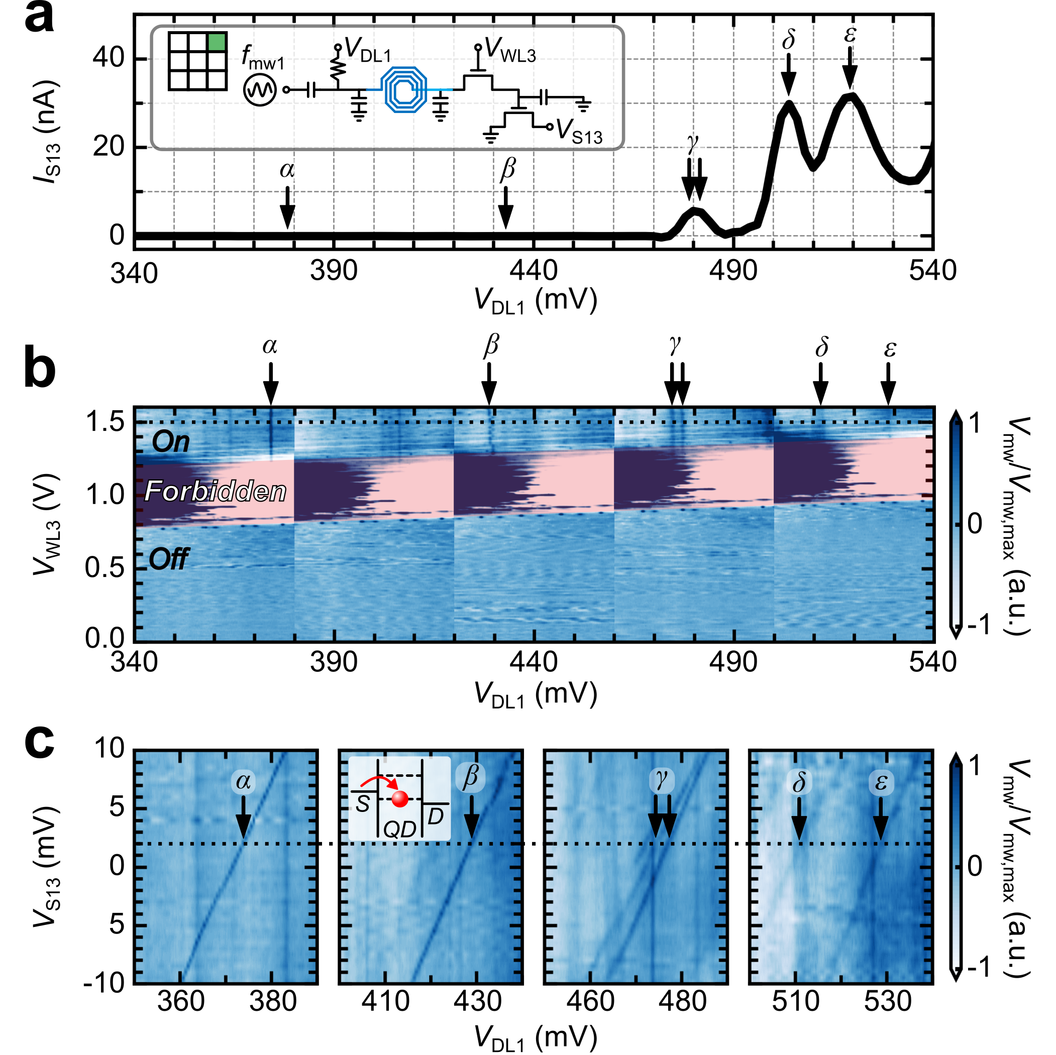
We use the resonators as sensors to perform integrated gate-based dispersive readout of the QD charge states. The resonators produce an oscillatory voltage on the gate of the QD which can result in cyclic tunneling of electrons back and forth the electronic reservoirs Ahmed et al. (2018b). This results in an equivalent capacitance that modifies the impedance of the resonator producing a change in the reflected voltage ().
To benchmark the method, we performed DC transport measurements, shown in Fig. 2a, for device , and observe Coulomb peaks , , and . We compare these results with those measured via reflectometry in the same region (Fig. 2b), while exploring the dependence with the state of the access transistor. At low V, the access transistor is highly resistive and the microwave signal is highly attenuated (Off region). At intermediate , the access transistor is in the depletion region and the oscillatory voltage at the transistor input produces changes in the capacitance that are picked-up as large changes in the reflected signal (Forbidden region). Finally, at high V, the access transistor presents a low resistance state and the microwave signal can travel through (On region), exciting cyclic tunneling in the QD, which manifests as regions of enhanced . Besides the same transitions as in Fig. 2a, two additional peaks, and , are observed. These are results of cyclic tunneling to one of the electron reservoirs only (as opposed to current, that requires sizable tunneling rates to both source and drain). This highlights the efficiency of gate-based sensing in detecting electronic transitions even if the QDs are offset from the center of the channel and present low tunnel rates to one ohmic contact. To provide further evidence of the nature of these transitions, we present individual - maps in Fig. 2c. The dependence on suggests that and peaks are originated from cyclic tunneling to the source. A lineshape analysis (see Methods) from the data in Fig. 2c, reveals a signal-to-noise ratio (SNR) of 28.7 in 400 ms of integration time and a tunnel rate to the source of 48.3 GHz.
These measurements represent the first demonstration of fully-integrated conditional gate-based readout of quantum dots implemented in an industrial CMOS technology.
Time-multiplexed readout
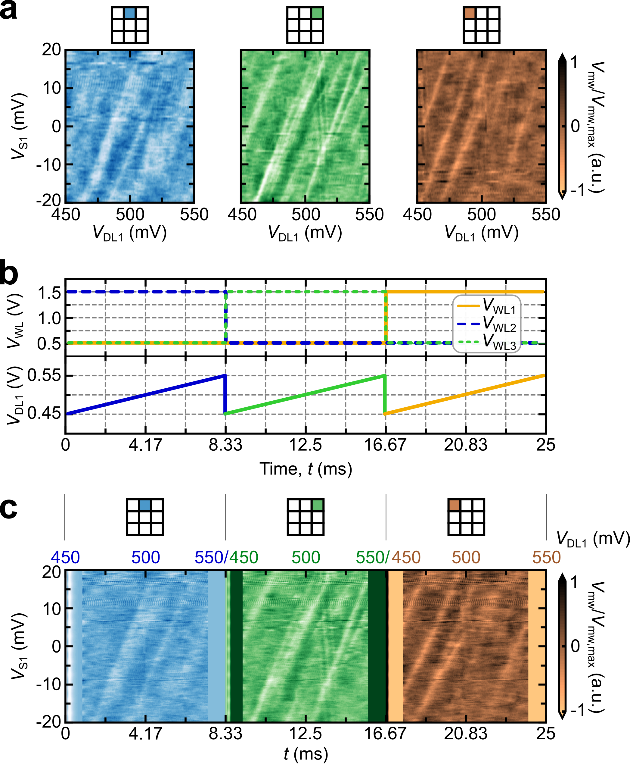
We then performed time-multiplexed reflectometry measurements of QD devices in the same row, by addressing them at the frequency of the shared resonator and activating the corresponding columns, one after the other. We chose with a carrier frequency = 6.872 GHz and used the 13 quantum dot array [].
We first measured the charge stability diagrams for each individual (Fig. 3a), when the corresponding access transistor is active. We used such data as the control set, we then performed the dynamic characterization in time-domain multiplexing and compared the results. The dynamic voltage sequence consists of a digital high voltage (=1.5 V) applied to the cell to be read, while the other two cells are set at low voltages (=0.5 V). The digital values are selected according to the On-Off regions in Fig. 2b. During that period, we simultaneously applied a voltage ramp to the data-line to acquire the data from the of the corresponding cell. We then sequentially raised the voltage of the next cell while keeping the other two low. The full sequence is illustrated in Fig. 3b, where we first measured followed by and . Finally, we repeated the full sequence as we stepped the voltages to acquire the charge stability maps in Fig. 3c. The match between the control set and the dynamic measurements indicates the success of the protocol.
We note that time-domain multiplexing does not necessarily require sequential addressing but can be performed in a random-access manner similar to DRAM architectures. These results represent fully-integrated time-multiplexed reflectometry measurements of silicon QDs and demonstrate an important reduction in the analog readout infrastructure of quantum circuits, since multiple devices can be read out by a single resonator.
Frequency-multiplexed readout
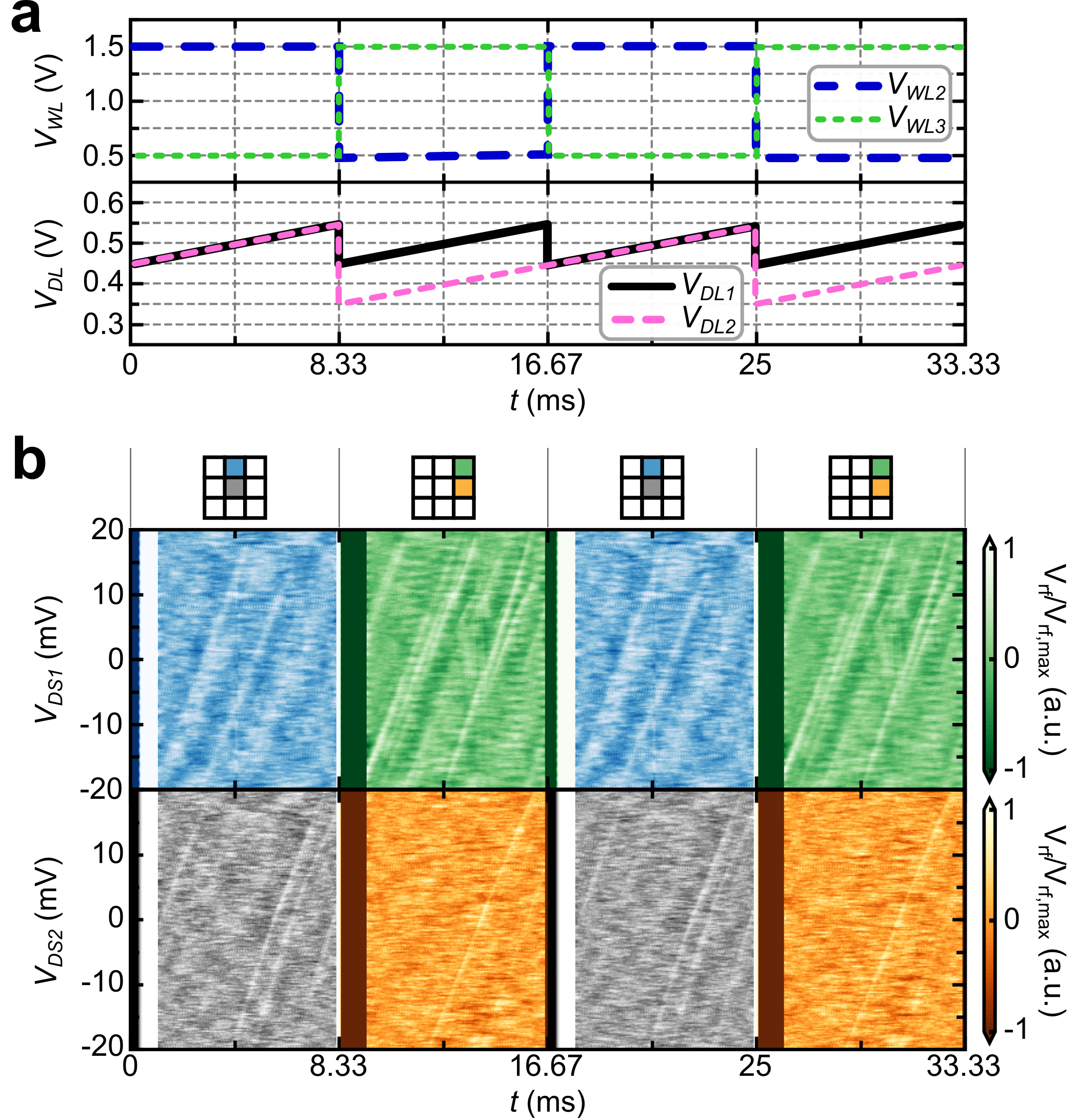
Once time-multiplexing (addressing columns) in reflectometry has been demonstrated, using the second degree of freedom in the matrix, we demonstrate frequency-multiplexing (addressing rows). For this experiment, we used at =7.419 GHz with at =6.873 GHz, to perform parallel readout of two independent QDs on different rows (addressable at different frequencies). As shown in Fig. 4a (left panels, up to 8.33 ms), the word-line voltage was kept high to activate column 2, while both and were ramped up to activate row 1 and 2. As a result, a 21 parallel set of Coulomb peak transitions from and was obtained (Fig. 4b, left panels, up to 8.33 ms).
Parallel readout reduces the overall integration time to read large quantum circuits by clustering in the same time step the readout of a number of devices. This feature is of particular relevance to quantum error correction sequences, such as the surface code, that requires continuous qubit readout at scale Fowler et al. (2012).
These results demonstrate fully-integrated frequency-multiplexing gate-based readout of silicon quantum dots on a single chip and in the 6-8 GHz range.
Time- and frequency-multiplexed readout
Finally, we combined time- and frequency domain multiplexing. and were used simultaneously for sensing the sub-arrays [, ] and [, ], respectively. Similar to the time-domain multiplexing readout, a sequence of square waves was applied to the word-lines, as shown in Fig. 4a, to selectively read out the transistors in different columns. Simultaneous arbitrary waves in and synchronized to and , as shown in Fig. 4a, were applied to read out two parallel rows. The result is a 22 matrix of Coulomb maps from the addressed quantum dots (Fig. 4b). The results presented here demonstrate, for the first time, the combination of time- and frequency-multiplexing gate-based readout for silicon QDs, in a fully-integrated platform, with a scalable architecture.
Conclusion
We have presented a cryogenic IC fabricated using industrial 40-nm CMOS technology that contains three elements required in a silicon-based quantum computer: QDs, I/O management and multiplexed readout electronics. Our results probe the limits of integration using commercial CMOS technology and pave the way to the realization of an integrated silicon quantum processor. On the way forward, spin control will require attention. Single qubit control could be achieved by embedding the IC in a 3D cavity to perform electron spin resonance conditionally controlled by Stark shifts Laucht et al. (2015). Two-qubit gates will require bringing the cells in close proximity to enable spin exchange interaction. Current industrial design rules for this process set the gate pitch limit to 120 nm, therefore some process customization will be required to bring it down to 70 nm, where sizeable tunnel coupling occurs Ansaloni et al. (2020). Finally, the SNR could be improved by lowering the tunnel rates closer to the probing frequency, by increasing the quality factor of the inductors using industry-compatible superconductors (TiN) Shearrow et al. (2018) and by using traveling-wave or Josephson parametric amplification Schaal et al. (2020). These improvements could reduce the minimum integration time by a factor of 100 or more, to bring it below the coherence time of the qubits Veldhorst et al. (2014), a necessity for error correction protocols.
References
- Arute et al. (2019) F. Arute et al., “Quantum supremacy using a programmable superconducting processor,” Nature 574, 505–510 (2019).
- Watson et al. (2018) T. F. Watson et al., “A programmable two-qubit quantum processor in silicon,” Nature 555, 633–637 (2018).
- Reilly (2015) D. J. Reilly, “Engineering the quantum-classical interface of solid-state qubits,” npj Quantum Information 1, 15011 (2015).
- Charbon et al. (2016) E. Charbon et al., “Cryo-CMOS for quantum computing,” in 2016 IEEE International Electron Devices Meeting (IEDM) (2016) pp. 13.5.1–13.5.4.
- Reilly (2019) D. J. Reilly, “Challenges in Scaling-up the Control Interface of a Quantum Computer,” in 2019 IEEE International Electron Devices Meeting (IEDM) (2019) pp. 31.7.1–31.7.6.
- Maurand et al. (2016) R. Maurand et al., “A CMOS silicon spin qubit,” Nature Communications 7, 13575 (2016).
- Montanaro (2016) A. Montanaro, “Quantum algorithms: an overview,” npj Quantum Information 2, 15023 (2016).
- Veldhorst et al. (2014) M. Veldhorst et al., “An addressable quantum dot qubit with fault-tolerant control-fidelity,” Nature Nanotechnology 9, 981–985 (2014).
- Urdampilleta et al. (2019) M. Urdampilleta et al., “Gate-based high fidelity spin readout in a CMOS device,” Nature Nanotechnology 14, 737–741 (2019).
- Yoneda et al. (2018) J. Yoneda et al., “A quantum-dot spin qubit with coherence limited by charge noise and fidelity higher than 99.9%,” Nature Nanotechnology 13, 102–106 (2018).
- Huang et al. (2019) W. Huang et al., “Fidelity benchmarks for two-qubit gates in silicon,” Nature 569, 532–536 (2019).
- Zajac et al. (2018) D. M. Zajac et al., “Resonantly driven CNOT gate for electron spins,” Science 359, 439–442 (2018).
- Fowler et al. (2012) A. G. Fowler et al., “Surface codes: Towards practical large-scale quantum computation,” Physical Review A 86, 032324 (2012).
- Kawakami et al. (2014) E. Kawakami et al., “Electrical control of a long-lived spin qubit in a Si/SiGe quantum dot,” Nature Nanotechnology 9, 666–670 (2014).
- Yang et al. (2020a) T.-Y. Yang et al., “Quantum Transport in 40-nm MOSFETs at Deep-Cryogenic Temperatures,” IEEE Electron Device Letters 41, 981–984 (2020a).
- Bonen et al. (2019) S. Bonen et al., “Cryogenic Characterization of 22-nm FDSOI CMOS Technology for Quantum Computing ICs,” IEEE Electron Device Letters 40, 127–130 (2019).
- Veldhorst et al. (2017) M. Veldhorst et al., “Silicon CMOS architecture for a spin-based quantum computer,” Nature Communications 8, 1766 (2017).
- Vandersypen et al. (2017) L. M. K. Vandersypen et al., “Interfacing spin qubits in quantum dots and donors-hot, dense, and coherent,” npj Quantum Information 3, 34 (2017).
- Li et al. (2018) R. Li et al., “A crossbar network for silicon quantum dot qubits,” Science Advances 4, 3960 (2018).
- Le Guevel et al. (2020) L. Le Guevel et al., “A 110mK 295W 28nm FDSOI CMOS Quantum Integrated Circuit with a 2.8GHz Excitation and nA Current Sensing of an On-Chip Double Quantum Dot,” in 2020 IEEE International Solid-State Circuits Conference - (ISSCC) (2020) pp. 306–308.
- Opremcak et al. (2018) A. Opremcak et al., “Measurement of a superconducting qubit with a microwave photon counter,” Science 361, 1239–1242 (2018).
- Yang et al. (2020b) C. H. Yang et al., “Operation of a silicon quantum processor unit cell above one Kelvin,” Nature 580, 350–354 (2020b).
- Petit et al. (2020) L. Petit et al., “Universal quantum logic in hot silicon qubits,” Nature 580, 355–359 (2020).
- Xue et al. (2020) X. Xue et al., “CMOS-based cryogenic control of silicon quantum circuits,” (2020), arXiv:2009.14185 [quant-ph] .
- Pauka et al. (2019) S. J. Pauka et al., “A Cryogenic Interface for Controlling Many Qubits,” (2019), arXiv:1912.01299 [quant-ph] .
- Hornibrook et al. (2014) J. M. Hornibrook et al., “Frequency multiplexing for readout of spin qubits,” Applied Physics Letters 104, 103108 (2014).
- Pauka et al. (2020) S. J. Pauka et al., “Characterizing Quantum Devices at Scale with Custom Cryo-CMOS,” Phys. Rev. Applied 13, 054072 (2020).
- Potočnik et al. (2020) A. Potočnik et al., “Millikelvin temperature cryo-CMOS multiplexer for scalable quantum device characterisation,” (2020), arXiv:2011.11514 [quant-ph] .
- Paquelet Wuetz et al. (2020) B. Paquelet Wuetz et al., “Multiplexed quantum transport using commercial off-the-shelf CMOS at sub-Kelvin temperatures,” npj Quantum Information 6, 43 (2020).
- Schaal et al. (2019) S. Schaal et al., “A CMOS dynamic random access architecture for radio-frequency readout of quantum devices,” Nature Electronics 2, 236–242 (2019).
- West et al. (2019) A. West et al., “Gate-based single-shot readout of spins in silicon,” Nature Nanotechnology 14, 437–441 (2019).
- Colless et al. (2013) J. I. Colless et al., “Dispersive Readout of a Few-Electron Double Quantum Dot with Fast rf Gate Sensors,” Phys. Rev. Lett. 110, 046805 (2013).
- Wallraff et al. (2004) A. Wallraff et al., “Strong coupling of a single photon to a superconducting qubit using circuit quantum electrodynamics,” Nature 431, 162–167 (2004).
- Zwanenburg et al. (2013) F. A. Zwanenburg et al., “Silicon quantum electronics,” Rev. Mod. Phys. 85, 961–1019 (2013).
- Ares et al. (2016) N. Ares et al., “Sensitive Radio-Frequency Measurements of a Quantum Dot by Tuning to Perfect Impedance Matching,” Phys. Rev. Applied 5, 034011 (2016).
- Samkharadze et al. (2018) N. Samkharadze et al., “Strong spin-photon coupling in silicon,” Science 359, 1123–1127 (2018).
- Mi et al. (2018) X. Mi et al., “A coherent spin-photon interface in silicon,” Nature 555, 599–603 (2018).
- Zheng et al. (2019) G. Zheng et al., “Rapid gate-based spin read-out in silicon using an on-chip resonator,” Nature Nanotechnology 14, 742–746 (2019).
- Ahmed et al. (2018a) I. Ahmed et al., “Radio-Frequency Capacitive Gate-Based Sensing,” Phys. Rev. Applied 10, 014018 (2018a).
- Gonzalez-Zalba et al. (2015) M. F. Gonzalez-Zalba et al., “Probing the limits of gate-based charge sensing,” Nature Communications 6, 6084 (2015).
- Ahmed et al. (2018b) I. Ahmed et al., “Primary thermometry of a single reservoir using cyclic electron tunneling to a quantum dot,” Communications Physics 1, 66 (2018b).
- Laucht et al. (2015) A. Laucht et al., “Electrically controlling single-spin qubits in a continuous microwave field,” Science Advances 1, e1500022 (2015).
- Ansaloni et al. (2020) F. Ansaloni et al., “Single-electron operations in a foundry-fabricated array of quantum dots,” Nature Communications 11, 6399 (2020).
- Shearrow et al. (2018) A. Shearrow et al., “Atomic layer deposition of titanium nitride for quantum circuits,” Applied Physics Letters 113, 212601 (2018).
- Schaal et al. (2020) S. Schaal et al., “Fast Gate-Based Readout of Silicon Quantum Dots Using Josephson Parametric Amplification,” Phys. Rev. Lett. 124, 067701 (2020).
- Beckers et al. (2018) A. Beckers et al., “Cryogenic MOS Transistor Model,” IEEE Transactions on Electron Devices 65, 3617–3625 (2018).
- Patra et al. (2020) B. Patra et al., “Characterization and Analysis of On-Chip Microwave Passive Components at Cryogenic Temperatures,” IEEE Journal of the Electron Devices Society 8, 448–456 (2020).
Methods
Chip design and implementation
The chip architecture was designed and simulated using Cadence Virtuoso, and industry-standard design tool for integrated circuit design and implementation. The initial design of quantum dot transistors, access transistors and passive elements, such as inductors, capacitors and resistors in the resonators and bias-tees, was based on existing device models at 300 K provided in the process design kit (PDK) of the 40-nm CMOS foundry. Subsequently, cryogenic models Beckers et al. (2018); Patra et al. (2020) have been used to establish more predictive circuit design at 1-4 K temperatures, based on modified compact models for transistors, adjusted lumped-element equivalent models for resistors, capacitors and inductors, and electro-magnetic (EM) simulations with modified cryogenic substrate for custom microwave signal lines and connections. This allowed to provide a closer prediction of the chip performance at 50 mK, given that no established models exist for cryogenic circuit design at 1-4 K, let alone deep-cryogenic temperatures of 50 mK. Final simulations of the chip operation and performance have been performed using Cadence Virtuoso with such custom-modified cryogenic models and Keysight ADS Momentum (an industry-standard 3D planar EM solver) for electro-magnetic simulations of the whole chip, including all microwave lines, resonators, input ground-signal-ground (GSG) pads, bond-wires and external printed-circuit board (PCB) substrate, using modified material properties for cryogenic operation. The physical layout implementation was also performed with Cadence Virtuoso, while the physical design verification in terms of design rule check (DRC) and layout versus schematic (LVS) was performed using Mentor Graphics Calibre. The chip was finally fabricated by a standard VLSI manufacturing process in 40-nm technology in a multi-project wafer (MPW) without any custom modification. The values of the circuit components in Fig. 1b are listed in Table 1.
Experimental setup
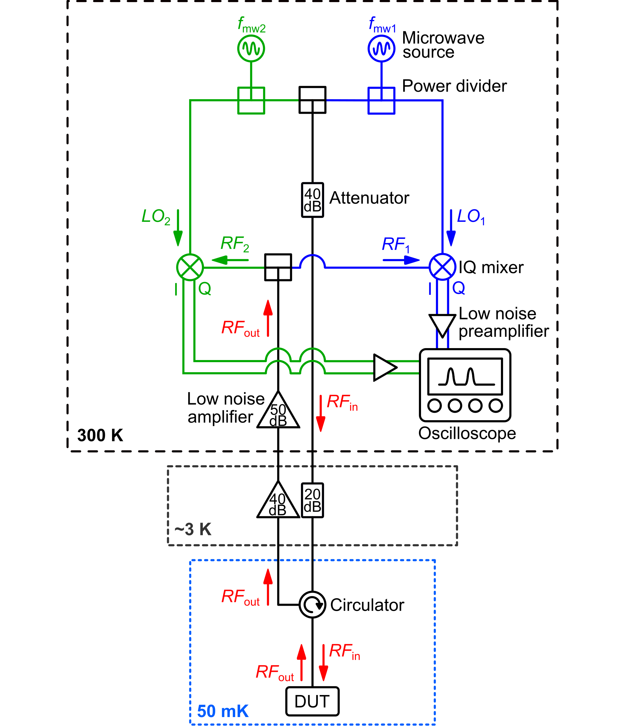
All the measurements reported at 50 mK were performed in an Oxford Instruments Triton 200 dilution fridge. The designed chip was glued to a PCB and wire-bonded to a microwave transmission line on board. The device under test (DUT) was placed on the sample stage of the dilution fridge. All DC measurements were performed using DC lines in the fridge connected to a room temperature parameter analyzer HP 4156A, and/or source measure unit (SMU) Keithley 2400, used to apply and measure source, gate, drain voltages and currents. The gate DC voltages were alternatively applied using voltage sources HP 3245A and Keysight 33500B. Reflectometry measurements were performed with a modified setup, including a discrete cryogenic amplifier (Low Noise Factory LNF-LNC4_8C) placed on a higher temperature stage (1-4 K), and a discrete cryogenic circulator (QUINSTAR QCY-G0400801) placed at the mixing chamber plate of the dilution fridge. A vector network analyzer (Rohde Schwarz ZVA 24) has been used to measure the frequency spectrum. To perform gate-based reflectometry measurements, externally, additional low-noise amplifiers (PASTERNACK PE1524 and/or PE1522) and an IQ mixer (Marki IQ-0618MXP) have been used at room temperature to perform signal demodulation. Microwave sources (Anritsu 3692B and 3694C) were employed to provide the local oscillator signal for down-conversion in a homodyne scheme, and an oscilloscope (Teledyne LeCroy HDO4054A) was used to acquire the IF signals after they were amplified by low noise pre-amplifiers (Stanford Research Systems SR560). For time-multiplexing, arbitrary waveform generators (Keysight 33500B) were used to generate the square wave and ramp signal sequences used for and , respectively. Finally, for (time- and) frequency-multiplexed measurements, two microwave signal sources have been used at room temperature with a power combiner (PASTERNACK PE2068) to generate multiplexed single-tone microwave probing signals towards the DUT and two IQ mixers have been used to demodulate the two tones separately by using the same microwave sources as local oscillators, respectively. The obtained signals have been acquired by the oscilloscope simultaneously. The complete setup is shown in Fig. 5.
Data processing
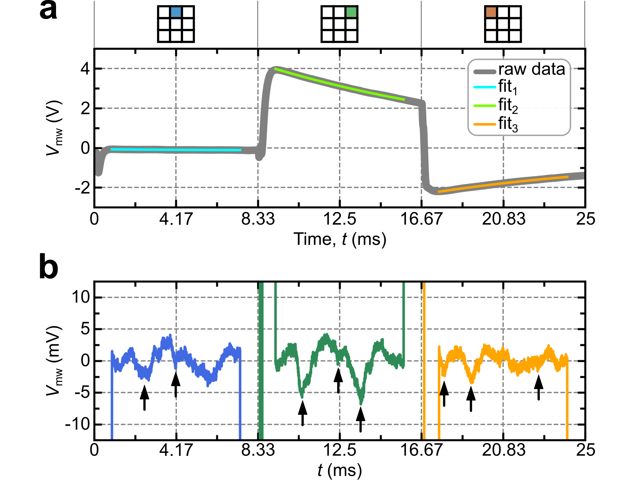
The time- (and frequency-)multiplexing readout data presented in this paper are processed data, and this is the data processing applied to it. In order to selectively address different columns in the quantum dot transistor array, square waves are applied to the word-lines when performing time-domain multiplexing readout. However, the rapid switches in the word-line voltages create large backgrounds which mask the reflectometry signals, as shown in Fig. 6a. Hence, we use polynomial fits to the data as backgrounds. After subtracting the backgrounds from the original data, as shown in Fig. 6b, the Coulomb blockade peaks are revealed and consistent with the individual reflectometry measurement for transistors , , and in Fig. 3a.
Data analysis
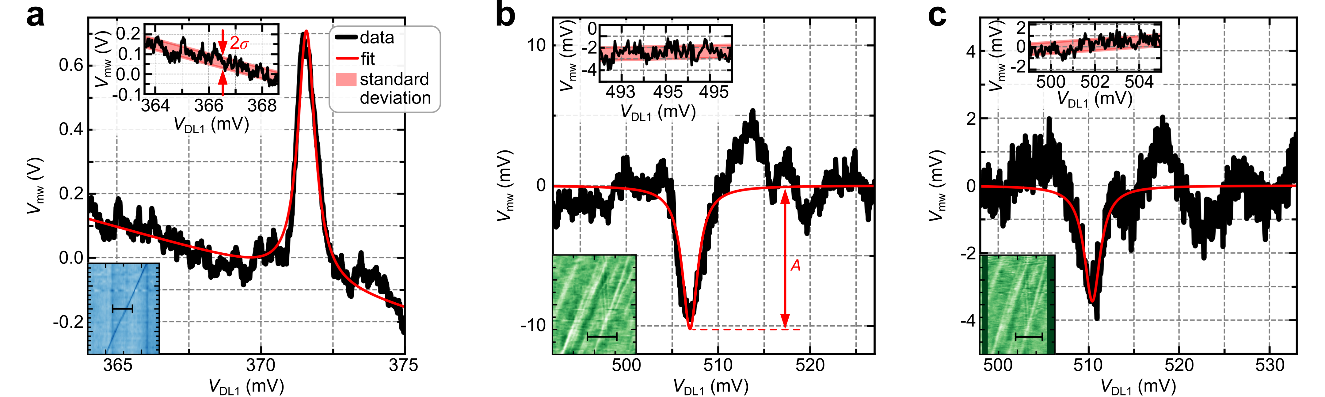
The signal-to-noise ratio (SNR) can be derived from the reflectometry signal , as shown in Fig. 7a, and SNR=A/=28.7, where is the Coulomb blockade peak amplitude and is the standard deviation of the noise signals. To extract the amplitude, we use a Lorentzian fit corresponding to the expected lineshape for lifetime broadened transitions Ahmed et al. (2018b):
| (1) |
where is the tunnel rate, the lever arm or gate coupling factor and the data-line voltage at which the source and gate Fermi levels align. We compare the individual device measurement and the time-domain multiplexing measurement in Fig. 7b and Fig. 7c respectively, and show a benchmark in Table 2. Furthermore, we estimate the minimum integration time (defined as the time to reach SNR=1) from the bandwidth of the measurement and the number of averages. The tunnel rate for Source-QD is estimated as well. These results are shown in Table 2.
Data availability
The data that support the plots within this paper and all the findings of this study are available from the corresponding author upon reasonable request.
Acknowledgments
We are grateful to Simon Schaal for providing useful comments.
The research leading to these results has received funding from the European Union’s Horizon 2020 research and innovation programme under grant agreement No. 688539 and 951852. M. F. G.-Z. acknowledges support from the Royal Society.
Author contributions
A. R., M. F. G.-Z. and E. C. conceived the architecture and devised the experiments; A. R. and Y. P. designed the chip with inputs from E. C. and M. F. G.-Z.; T.-Y. Y., J. M., M. F. G.-Z. and A. R. performed the experiments and analyzed the results; A. R., T.-Y. Y. and M. F. G.-Z. wrote the manuscript with inputs from all the coauthors, M. F. G.-Z. and E. C. supervised all the experiments.
Competing interests
The authors declare no competing interests.
Additional information
Supplementary information is available for this paper.
Correspondence should be addressed to A. R. (andrea.ruffino@epfl.ch).
Request for materials should be addressed to T.-Y. Y. (tyy20@cam.ac.uk).
Supplementary Information
S1. Retention time study
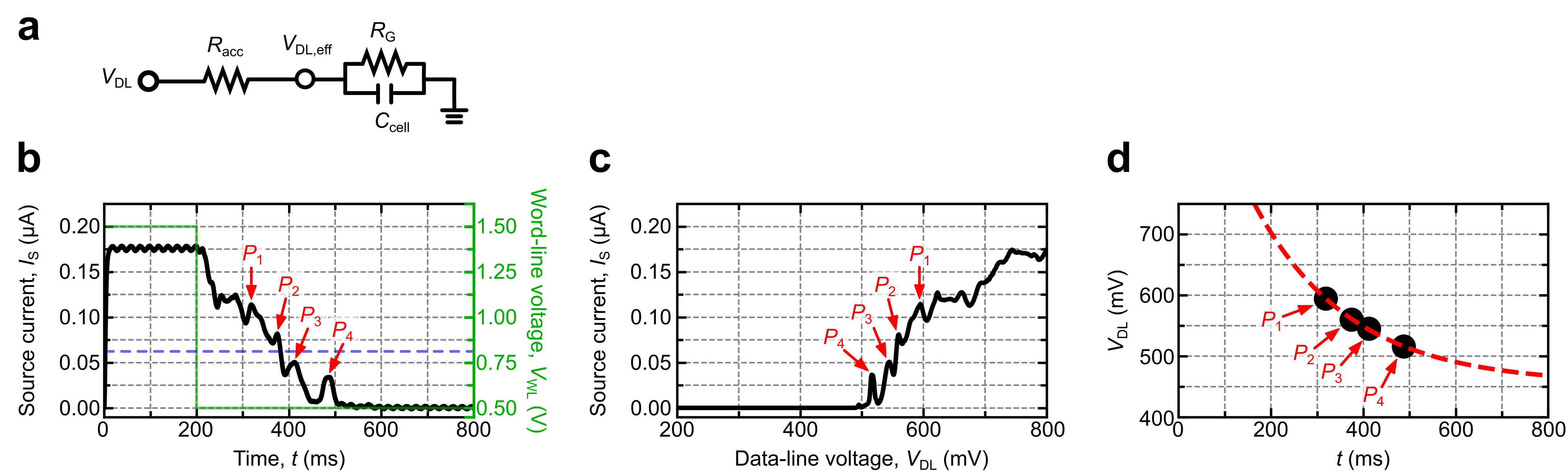
We characterize the charge retention time for an individual cell at 50 mK. A simple equivalent circuit model is shown in Fig. 8a Schaal et al. (2019). To extract the retention time, we apply the sequence (i) charging and (ii) discharging. For (i) charging: the cell is firstly charged by applying =1.49 V, much higher than the threshold voltage of the access transistor, while =0.8 V, as in Fig. 8b, setting the access transistor well in the ON state. This is then followed by (ii) discharging: is reduced to 0.5 V, where the access transistor is highly resistive. The effective voltage on the QD transistor gate as a function of time can be expressed as:
| (2) |
where is the equilibrium voltage at the QD transistor gate at , and and are the gate leakage resistance of the QD transistor and the channel resistance of the access transistor, respectively. is the circuit time constant, i.e., retention time, where is the parallel sum of the QD transistor gate capacitance and storage capacitance in Fig. 1b. By monitoring after is switched from 1.49 V to 0.5 V, Coulomb oscillations are observed as a function of time due to the decay of in time, as shown in Fig. 8b. The observed Coulomb peaks in the time domain, marked as , , , and , have their counterparts in the voltage domain, as shown in Fig. 8c. Combining the marked Coulomb peaks in time and voltage domains, we fit the data points to Equation (2) and find the time constant 207 ms in this cell, as shown in Fig. 8d. From Fig. 1d in the main text, we deduce that at =0.5 V, and leakage occurs primarily through the gate resistance of the QD device. Considering =200 fF, we obtain 1 T. Further improvements in the gate voltage retention time will require increasing .
It is also worth mentioning that limited charge injection is visible in Fig. 8b after switching. The design only uses a single nMOS pass transistor, instead of a transmission gate (nMOS and pMOS) for the access transistor, but additional dummy single-finger transistors have been included in the layout next to the access transistor to absorb and minimize the charge injected by switching.
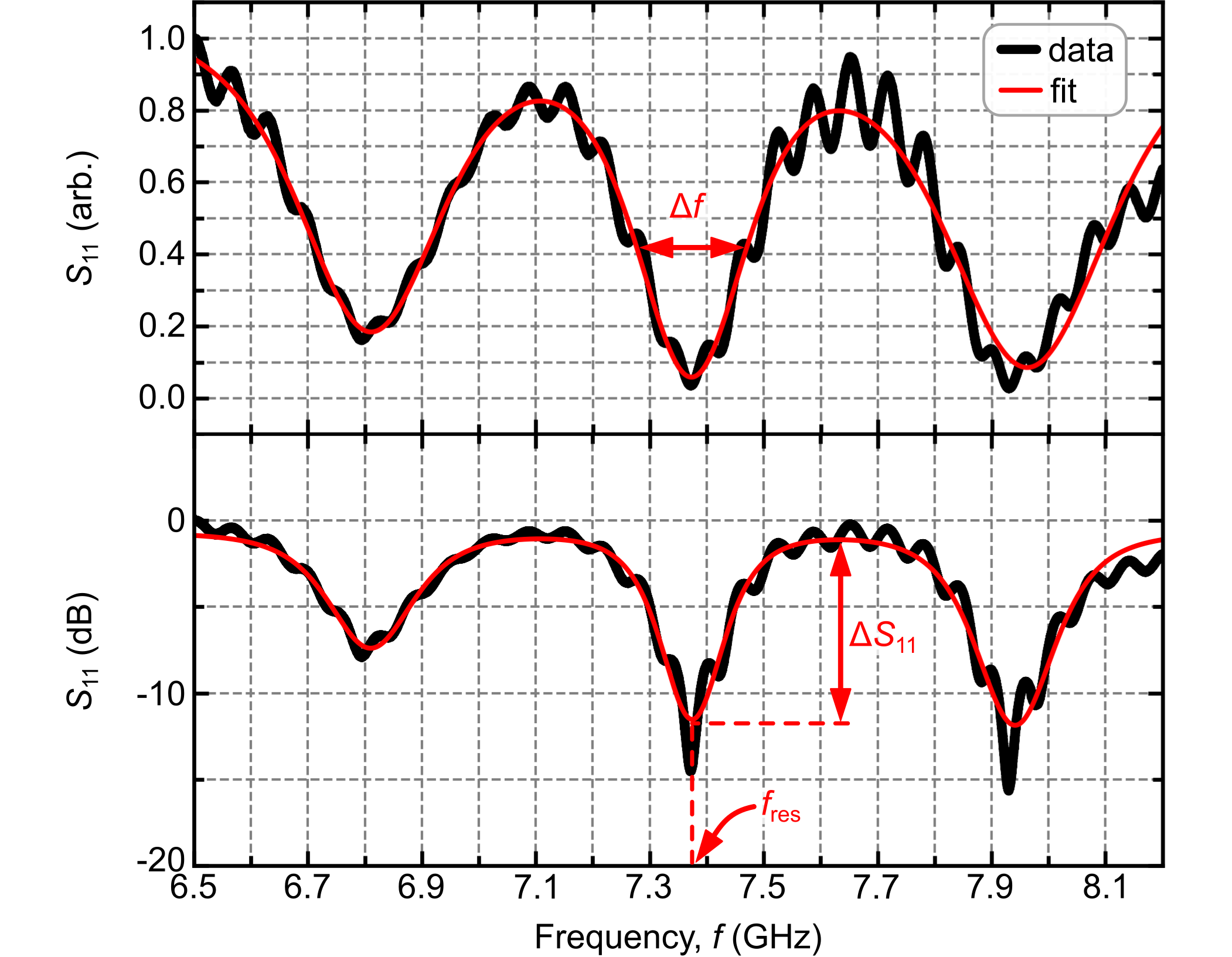
S2. Resonator characterization at room temperature
We characterize the integrated LC resonators by measuring the frequency spectrum, as shown in Fig. 9. We perform the measurement at room temperature by directly connecting a VNA to the microwave port on the PCB (Set-up A). We perform numerical fittings to the data by initially estimating the resonance frequencies () where the reflection coefficient has local minima, i.e., around (6.8, 7.4, 7.9) GHz for (, , ), respectively. The resonance frequencies and the reflection coefficients at the resonance frequencies () are then extracted from the fitted results (red curves in Fig. 9). Furthermore the quality factors (Q) can be derived from , where is the full width at half maximum of the fit. The characteristics of the three integrated resonators are listed in Table 3.
It is worth mentioning that the resonators on chip are, instead of more conventional L-shaped LC matching networks, CLC matching networks (, , ), since the former would impose a fixed matching network quality factor determined by the ratio of source (50 ) and load impedance (the gate of the QD device), while the latter introduces an additional degree of freedom, thus allowing to independently determine the matching network quality factor. Therefore, all components in the matching network are functional, not due to parasitics. Finally, however, the measured quality factor is in any case determined by the component quality factor, in this case mostly by inductors.
Extended Data
![[Uncaptioned image]](/html/2101.08295/assets/figures/Table1_2021-01-16.png)
![[Uncaptioned image]](/html/2101.08295/assets/figures/Table2_2021-01-16.png)
![[Uncaptioned image]](/html/2101.08295/assets/figures/Table3_2021-01-16.png)