QUBIC IV: Performance of TES Bolometers and Readout Electronics
Abstract
A prototype version of the Q & U bolometric interferometer for cosmology (QUBIC) underwent a campaign of testing in the laboratory at Astroparticle Physics and Cosmology laboratory in Paris (APC). The detection chain is currently made of 256 NbSi transition edge sensors (TES) cooled to 320 mK. The readout system is a 128:1 time domain multiplexing scheme based on 128 SQUIDs cooled at 1 K that are controlled and amplified by an SiGe application specific integrated circuit at 40 K. We report the performance of this readout chain and the characterization of the TES. The readout system has been functionally tested and characterized in the lab and in QUBIC. The low noise amplifier demonstrated a white noise level of 0.3 . Characterizations of the QUBIC detectors and readout electronics includes the measurement of I-V curves, time constant and the noise equivalent power. The QUBIC TES bolometer array has approximately 80% detectors within operational parameters. It demonstrated a thermal decoupling compatible with a phonon noise of about at 410 mK critical temperature. While still limited by microphonics from the pulse tubes and noise aliasing from readout system, the instrument noise equivalent power is about , enough for the demonstration of bolometric interferometry.
1 Introduction
QUBIC is an international ground based experiment dedicated to the observation of cosmic microwave background (CMB) polarisation. It will be deployed in Argentina, at the Alto Chorrillos mountain site (altitude of 4869 m a.s.l.) near San Antonio de los Cobres, in the Salta province. QUBIC has two configurations: the “technological demonstrator” (TD) and the “full instrument” (FI). The TD and FI share the same cryostat and cryogenics but the TD has only one-quarter of the 150 GHz TES focal plane (256 TESs), an array of 64 horns and switches and a smaller optical combiner. The QUBIC TD has demonstrated the feasibility of the bolometric interferometry after extensive tests at APC laboratory since 2018. In this paper, we present the main results of this characterization phase on the detection chain.
This paper is organized as follows. An overview of the QUBIC detection chain is given in Section 2. The tests of the readout system is described in Section 3. Section 4 describes the TES characterizations in terms of critical temperature, TES parameters, power background, time constants and noise performance. Finally, some concluding remarks are given in Section 5.
2 QUBIC detection chain
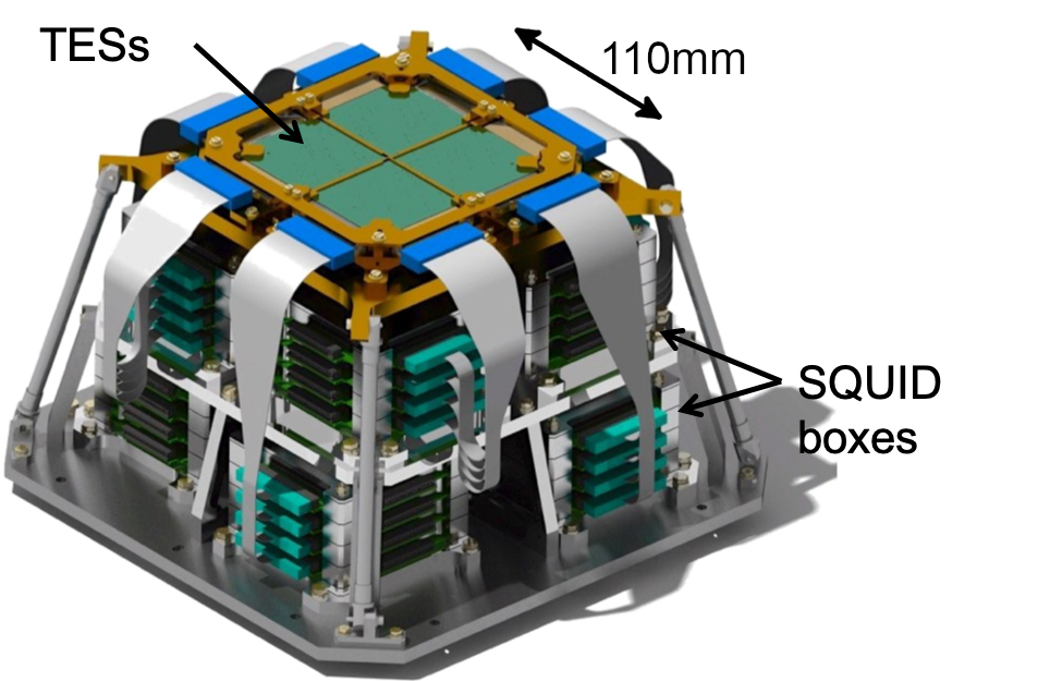
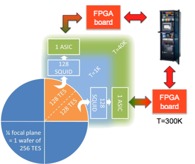
The QUBIC detection chain architecture is shown on Figure 1. Each focal plane is composed of four 256-pixel TES arrays assembled together to obtain 1024-pixel detector cooled at about 320 mK by a 3He fridge. For each quarter focal plane, two blocks of 128 SQUIDs (superconducting quantum interference devices) are used at 1 K in a 128:1 time domain multiplexing (TDM) scheme [1, 2]. Each block is controlled and amplified by an ASIC (application specific integrated circuit) cooled to 40 K while a warm FPGA (field programmable gate array) board ensure the control and acquisition of the signal to the acquisition computer.
2.1 TES
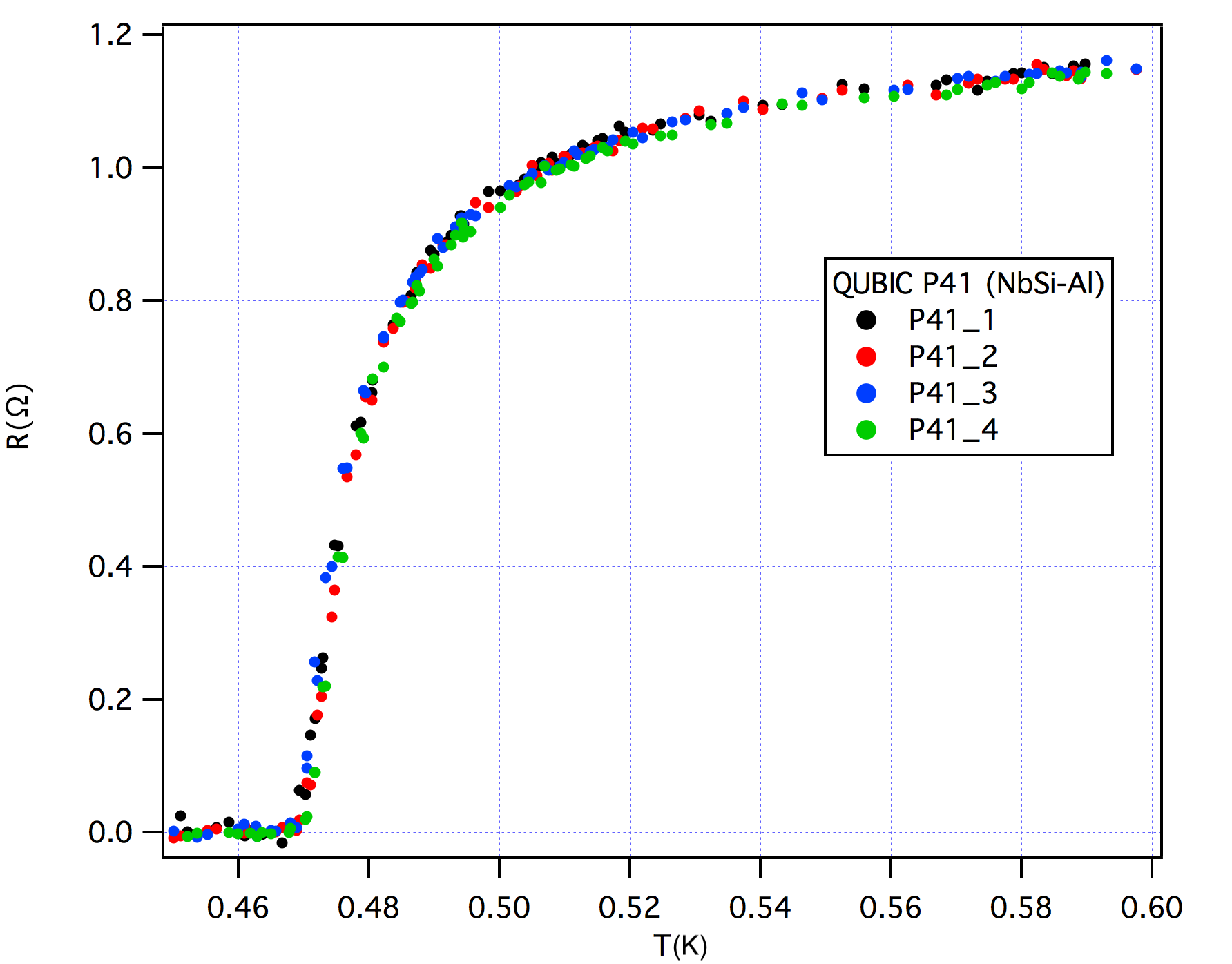
The detectors are TESs made with a NbxSi1-x amorphous thin film (x0.15 in our case). Their transition temperature Tc (Figure 2) can be adapted by changing the composition of the compound. The array currently used (reference P87) has a critical temperature of about 410 mK. The normal state resistance Rn is adjusted to about 1 with interleaved electrodes for optimum performance. To adapt to the optics, the pixels have 3 mm spacing while the grid absorber structure is 2.7 mm wide without sensitivity to polarization.
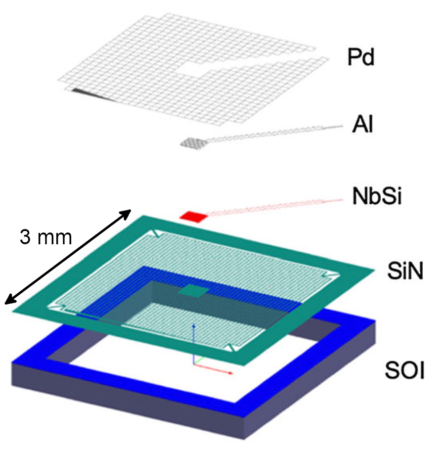
The low thermal coupling between the TES and the thermal bath is obtained using 500 nm thin SiN suspended and patterned membranes, which exhibit thermal conductance in the range 50-500 pW/K depending on the precise pixel geometry and temperature. The noise equivalent power (NEP) is expected to be of the order of at 150 GHz with a natural time constant of about 100 ms [3]. Light absorption is achieved using a Palladium metallic grid placed in a quarter-wave cavity optimizing the absorption efficiency. The back-short distance of 400 m has been chosen after electromagnetic simulations in order to have absorption higher than 94% at both 150 and 220 GHz. The routing of the signal between the TES and the bonding pads at the edge of the array is realised by superconducting aluminium lines patterned on the silicon frame supporting the membranes. The detailed fabrication process of the QUBIC detectors is given in [4]. The latest upgrade of the production process allows excellent fabrication quality with a dead-pixel yield as low as 5% at room temperature.
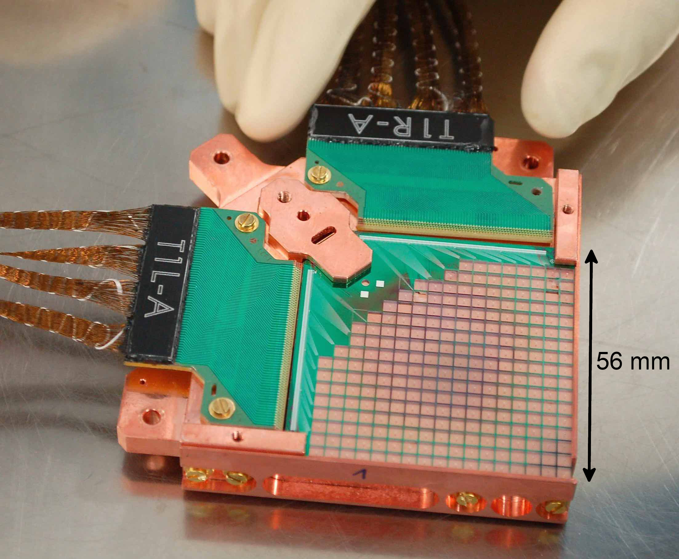
The 256-pixel array is finally integrated within the focal plane holder and electrically connected to an aluminium printed circuit board (PCB, provided by Omni Circuit Boards111www.omnicircuitboards.com) using ultrasonic bonding of aluminium wires (Figure 3).
2.2 SQUIDs
The second stage of the detection chain is composed of the SQUIDs maintained at a temperature of about 1 K by a 4He fridge. Each TES is in series with the input inductance of the SQUID and is voltage biased with a resistor in parallel as shown in Figure 4. The input inductance of the SQUID converts the TES current into a magnetic flux that is converted in an output voltage by the SQUID. The latter is therefore a trans-impedance amplifier with a gain of the order of 100 V/A. To compensate the flux variation, a current from a feedback loop is injected to create a feedback flux . The voltage sent by the digital to analog converter (DAC) to create this feedback current through the feedback resistor is the QUBIC signal (Figure 4). This process, allowing to lock the flux operating point in the SQUID is known as a flux locked loop (FLL) [5].
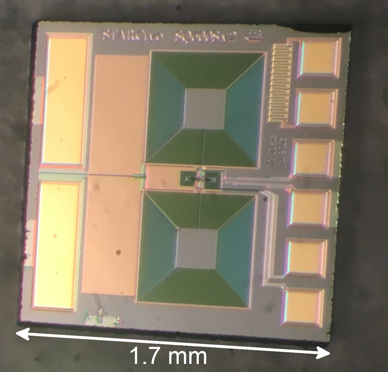
In addition to being cryogenic amplifiers, SQUIDs also enable the multiplexing because of their large bandwidth. As shown in Figure 5, the SQUID multiplexer is composed of 4 columns of 32 SQUIDs AC-biased with capacitors in order to reduce power dissipation and noise. The SQUIDs used in QUBIC shown in Figure 6 have a dual-washer gradiometric layout. They are based on a SQ600S commercial design provided by StarCryoelectronics222starcryo.com, slightly modified in order to reduce the area of each die.
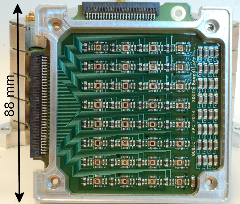
Visual inspections and room temperature tests with a probe-station are used to select the SQUIDs before integration on a specific PCB. One SQUID PCB is composed of 32 SQUIDs and is integrated in an aluminium box. The architecture therefore uses 4 of these PCB boxes to read out 128 pixels. As shown in Figure 1, 4 stack of 8 SQUID boxes is installed at 1 K below the TESs in the cryo-mechanical structure, surrounded with a Cryophy333www.aperam.com magnetic shield.

2.3 ASIC
In addition to the SQUIDs, a 4 to 1 multiplexed low noise amplifier (LNA) reads out sequentially 4 columns of 32 SQUID each. The resulting multiplexing factor is 128. The LNA, together with sequential biasing of the SQUID and the overall clocking of this 128:1 multiplexer, is all done in a cryogenic ASIC operating at about 40 K [6]. The TDM readout is based on the association of 4 columns of 32 SQUIDs in series with the dedicated cryogenic ASIC.
The ASIC is designed in full-custom using CADENCE CAD tools. The technology is a standard m BiCMOS SiGe from Austria MicroSystem (AMS). This technology consists of p-substrate, 4-metal and 3.3 V process. It includes standard complementary MOS transistors and high speed vertical SiGe NPN hetero-junction bipolar transistors (HBT). Bipolar transistors are preferentially used for the design of analog parts because of their good performance at cryogenic temperature [1]. The design of the ASIC is based on pre-experimental characterizations results, and its performance at cryogenic temperature is extrapolated from simulation results obtained at room temperature, using CAD tools.
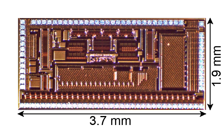
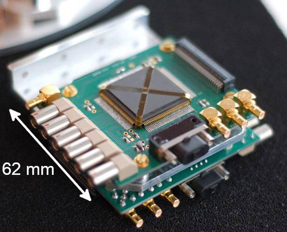
Each ASIC board (shown in Figure 7) has a power dissipation of typically 16 mW and is placed on the 40-K stage. The ASIC integrates all parts needed to achieve the readout, the multiplexing and the control of an array of up to 128 TESs/SQUIDs. It includes a differential switching current source to address sequentially 32 lines of SQUIDs, achieving a first level of multiplexing of 32:1. In this configuration, the SQUIDs are AC biased through capacitors which allows good isolation (low cross-talk between SQUID columns) and no power dissipation. A cryogenic SiGe low-noise amplifier ( 0.3 nV/, gain = 70, bandwidth of about 6 MHz in simulations) with 4 multiplexed inputs, performs a second multiplexing stage between each of the 4 columns. The low frequency noise of the LNA increases with decreasing temperature. An operation at about 40 K appears to be a good trade-off between this corner frequency and the white noise level.
This cryogenic ASIC includes also the digital synchronization circuit of the overall multiplexing switching (AC current sources and multiplexed low-noise amplifier). A serial protocol allows focusing on sub-array as well as adjusting the amplifiers and current sources with a reduced number of control wires. We have developed a full-custom CMOS digital library dedicated to cryogenic applications and ionizing environments (rad-hard full custom digital library) [1].
2.4 Warm electronics and acquisition software
The final stage of the readout electronics operates at room temperature on a board called NetQuiC. It is connected to the acquisition computer via a network switch. Each NetQuiC board is based on a differential amplifier (gain = 100, bandwidth limited to 1 MHz with a second-order anti aliasing low-pass filter), a 2 MHz 16-bit analog to digital converter (ADC), seven 16-bit DACs and a Xilinx Spartan 6 FPGA (XEM6010 board from Opal Kelly). It also contains 2 feedback resistors of 10 k and 100 k that could be individually connected for large dynamic range or sensitive measurements respectively. This system is designed to adjust the operating biasing of the TESs and to control the feedback of the SQUIDs. Moreover, it takes the signal from the cryogenic multiplexing ASIC, computes the scientific signal and sends it to the data acquisition system. For this detection chain each FPGA manages 128 detectors, with a total of 16 FPGAs for the full 2048 pixel focal planes. A dedicated software named QUBIC Studio was developed at the Institute for Research in Astrophysics and Planetology (IRAP) for the data acquisition [7, 2]. QUBIC Studio interfaces with the generic electrical ground support equipment (EGSE) tool, called “dispatcher”, which was also developed at IRAP. QUBIC Studio has a user-friendly interface to manage the connection with the readout electronics. This tool gives a global visualization of the complete detection chain.
3 Readout tests and characterization
The core of the readout is made of an ASIC cooled to 40 K that controls the multiplexing and amplifies the voltage from the SQUIDs. This device has been first tested and validated since it has been used to further characterize the SQUIDs.
3.1 ASIC tests and characterizations
3.1.1 Implemented functions
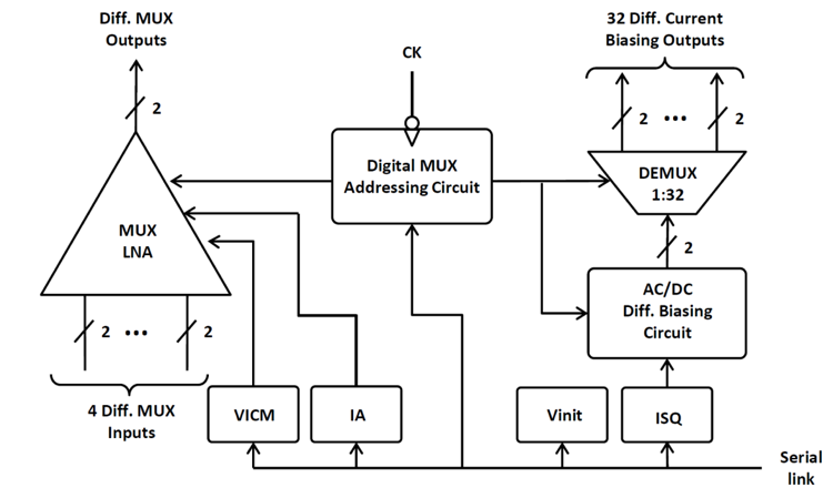
The ASIC called SQMUX128evo has been designed to control the time-domain multiplexing and to amplify the signals from 4 columns of 32 SQUIDs in series (see Figure 5) i.e. 128 channels. Its block diagram is outlined on Figure 8. The following functions have been integrated:
-
•
An ultra low noise voltage amplifier with 4 multiplexed inputs for reading 4 columns of SQUIDs,
-
•
a current source for the polarization of the multiplexed amplifier,
-
•
an AC bias current source associated with a 1:32 multiplexer for addressing the 32 SQUIDs lines through addressing capacitors,
-
•
two voltage references for adjusting the common mode at the input of the multiplexed amplifier and at the output of the AC bias source of the SQUID,
-
•
a digital circuit which controls the row / column addressing of the multiplexer from an external clock signal CK,
-
•
a serial link for addressing configurable blocks such as voltage references, bias current sources or the multiplexer’s row/column addressing circuit.
This ASIC has been integrated on a specific PCB in order to be fully characterized at room and cryogenic temperatures. It has been tested and proven functional down to 4.2 K thanks to a low power dissipation of about 16 mW per ASIC whatever the number of columns to read out. In QUBIC, the ASIC operates at approximately 40 K due to the available cryogenic power.
3.1.2 Current sources and voltage references
The ASIC SQMUX128evo integrates digitally adjustable current sources and voltage references for the biasing of the multiplexed input amplifier and for the SQUID AC bias circuit. The current sources are based on a fixed current reference (A typically) followed by current DACs whose values are encoded on 3 and 4 bits for the amplifier bias and the SQUID AC bias circuit respectively. The reference current is obtained by taking the current flowing through an external resistor under a fixed voltage (forward-biased diode voltage, about 0.7 V at room temperature). This allows to precisely adjust the reference current value according to the operating temperature. For a nominal current A:
-
•
The output of the 3-bit current DAC allows to adjust the bias of the amplifier with multiplexed inputs (IA in Figure 8) from 1.65 mA to 2.85 mA in steps of 200 A;
-
•
The output of the 4-bit DAC in current adjusts the AC bias of the SQUIDs (ISQ in Figure 8) from 5 A to 40 A in steps of 2.5 A.
The ASIC SQMUX128evo also incorporates two 3-bits voltage references for common mode adjustment at the input of the multiplexed amplifier (VICM) and at the output of the SQUID AC bias source (Vinit). This voltage ranges from 1.453 V to 1.895 V.
For the voltage references and current sources, the values measured at room temperature are fully compliant to those simulated. At low temperatures, an adjustment of the reference resistance and of the threshold voltage of a forward-biased diode from 0.7 V to about 1 V needs to be done to reproduce the results in simulation for the current sources. The agreement between measurement and simulation has been achieved thanks to the use of a proven standard technology with a reliable design kit.
3.1.3 Amplifier with 4 multiplexed inputs
The amplifier is made of 4 differential pairs of SiGe bipolar transistors (each with a trans-conductance ) whose collectors are connected to a common resistor ( at room temperature and at 40 K). The multiplexing is achieved by means of a set of CMOS switches that sequentially bias each differential pair that has to be activated ( typically). A common mode (VICM) is applied at the input of each differential pair through 2 series resistors of each (differential input impedance of ) connected to a 3-bit voltage reference. Each output of the differential stage is followed by a common collector amplifier in order to reduce the output impedance to about at low temperature. The expected maximum gain is about 20 and 70 at room and cryogenic temperature respectively.
Gain and noise measurements were performed using an Agilent444http://www.agilent.com HP89410 vector analyser. For the gain measurement, as the vector analyser does not have differential sources and inputs, the setup uses a ”single to differential” circuit, made from an AD8132, to differentiate the signal coming from the analyser source and drive the input of the amplifier under test. The output common mode of the AD8132 is adjusted to match the VICM of the amplifier under test. A Stanford Research SR560 amplifier is used to differentiate between the outputs of the amplifier under test before feedback to the input of the analyser. This external amplifier limits the bandwidth to about 1 MHz. For noise measurement, this amplifier is also used to provide the extra gain needed to overcome the noise floor of the analyser. In addition, the noise measurement is performed by shunting the differential inputs of the amplifier under test with a short circuit in the lab or with zero bias of the SQUIDs in QUBIC. The amplifier with multiplexed inputs is biased at maximum current (1.80 mA at 300 K and 2.85 mA at 77 K) so that the voltage gain is as high as possible.
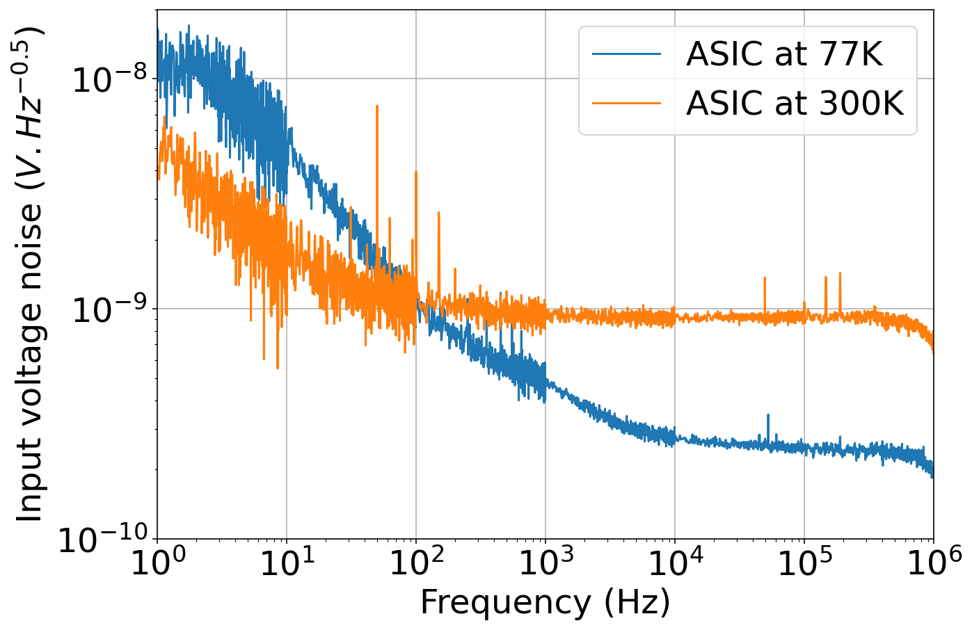
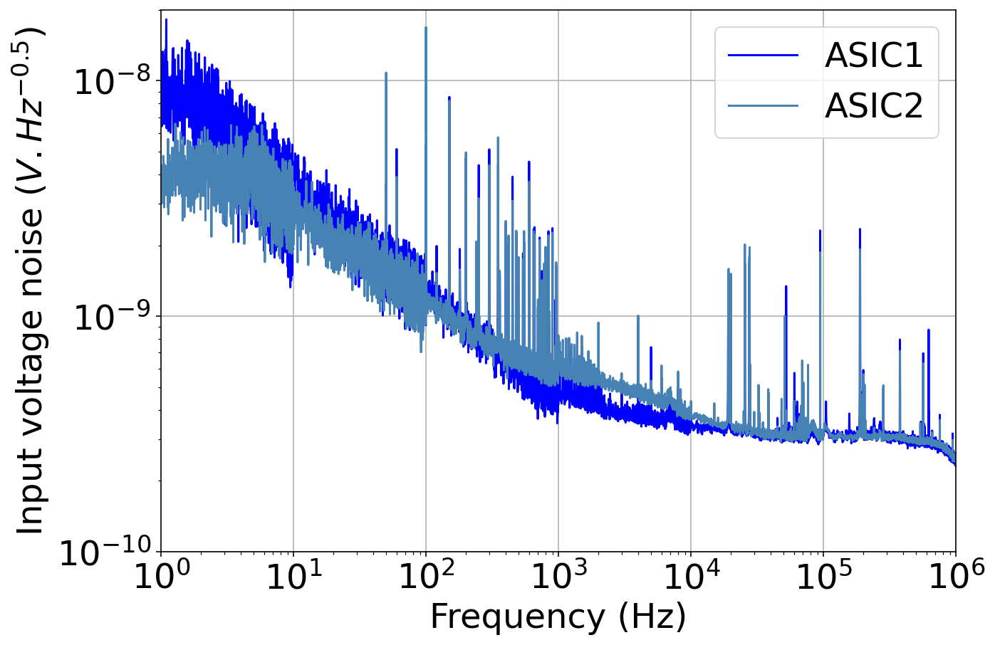
From 300 K to 77 K, the voltage gain increases from 20 to 70 as expected and the white noise level decreases from 0.95 nV/ to 0.25 nV/ as shown in Figure 9. The corner frequency also increases from about 100 Hz at room temperature to about 6 kHz at 77 K. The presence of an excess noise below 100 Hz at low temperature is not understood. The 3 dB bandwidth of the LNA is estimated at about 6 MHz by simulation, not measured precisely because of the limitation from the measurement setup.
3.1.4 AC bias current source
The AC bias current source allows to alternately bias two consecutive SQUIDs of the same row at + and - through addressing capacitors (no power dissipation on the cryogenic stages as compared to the addressing with resistors). It consists of two differential branches, each of them having an inverter degenerated by current mirrors referenced to the biasing current source described above. These inverters are controlled in phase opposition to the rate imposed by the column changes. Alternately, the outputs of these inverters simultaneously push and pull the same biasing current through each SQUID of the same row through the addressing capacitors. A 1:32 multiplexer located at the output of the inverters of the AC source allows the selection of the row to be biased. In order to avoid a drift of the operating point at the output of the inverters of the AC biasing circuit and a risk of saturation of the current sources, these outputs are connected to the voltage reference through 2 external resistors of 10 k.
3.1.5 Multiplexer addressing circuit
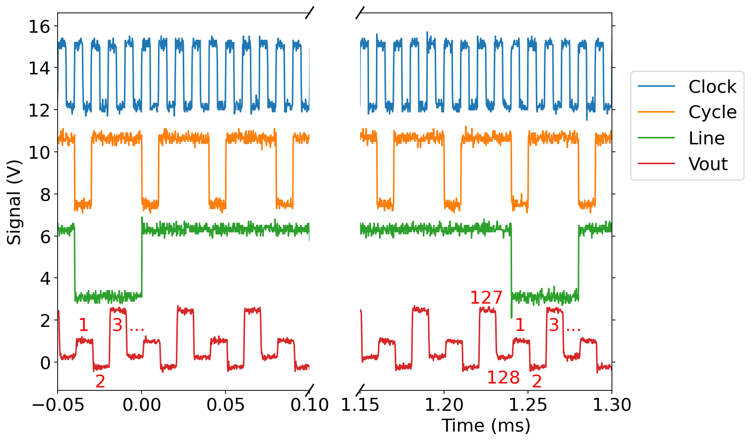
The sequencing of the multiplexing is carried out internally in the ASIC by an integrated digital circuit referenced to an external clock signal CK of 100 kHz nominal frequency. In addition to the control of the LNA and the SQUID biasing circuit, it generates two signals active on falling edge, SYNCCb and SYNCLb, that indicate the end of row and complete cycle respectively. The addressing circuit clocked at a multiplexing frequency of 100 kHz was functionally tested down to a temperature of 4.2 K as shown in Figure 10 [8].
3.1.6 Functional tests of the ASIC with SQUIDs
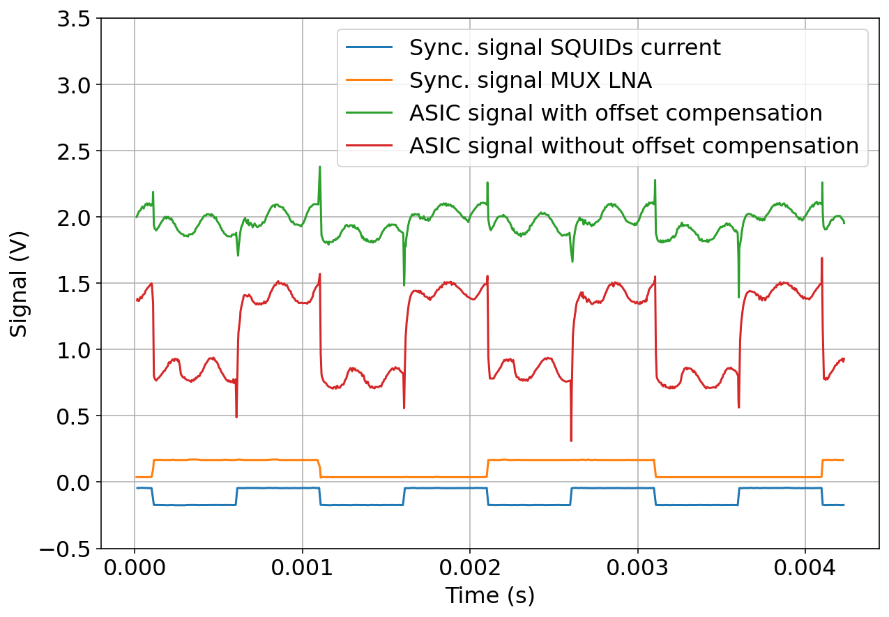
Functional tests of the ASIC have been performed down to 4.2K in a dedicated cryostat on a small array of 2 columns of 2 SQUIDs in series as shown in Figure 10. The settle time of the system after switching from one channel to the other is of the order of 5 s. These tests have validated the AC SQUID biasing operation and the overall multiplexing topology (switching AC current sources, multiplexed LNA and digital clocking).
3.2 SQUIDs tests and characterizations
The SQUIDs are first selected with room temperature measurements and furthermore characterized at two temperatures in the QUBIC readout system.
3.2.1 Selection and sorting of SQUIDs at 300 K
Before installation in QUBIC, the manufactured SQUIDs undergo a visual inspection in a clean room in order to detect and remove the ones exhibiting evidence of defects during fabrication or storage. We further proceed in the measurement of 4 resistance values at room temperature: heater, SQUID washer, feedback inductance and input inductance. The distribution of these values is found to be close to a Gaussian with a standard deviation of about 5% the mean value. SQUIDs with all parameters within 2 of the mean values are selected for installation in QUBIC. SQUIDs that are between 2 and 3 for one or more measurements are held aside as a possible option in case there are not enough SQUIDs passing the first criteria. All SQUIDs with any parameter larger than 3 from the mean are rejected. While these room temperature measurements do not guarantee that a SQUID is functional, the 2 and 3 selection process has been chosen as a trade-off between the number of available chips and the expected homogeneity in the SQUID behaviour. A further selection process is performed based on the leakage resistance between SQUID washer and the input inductance. Leakage measured at cryogenic temperature is typically a few M between a full stack of 32 SQUIDs and the 32 input inductances. This level of leakage does not significantly degrade the operation of the SQUIDs. The pass/fail level for leakage to the input inductance was therefore set at 2 M, with the majority of leakage values measured closer to 20 M. SQUIDs with leakage to the input inductance less than 2 M were rejected in order to avoid any risk of electrostatic discharge damage. For the same reason, the leakage between the SQUID washer and the feedback must be that of an open circuit (), otherwise the SQUID is rejected. We typically obtained a yield of about 82% for tested SQUIDs.
3.2.2 Tests at Cryogenic Temperature
The characterization of the SQUIDs is performed at the begining of the calibration phase, with the focal plane temperature kept just above the TES critical temperature in order to be in normal state and to reduce the detector current noise contribution. The main goal is to define the optimal SQUID bias current to be used during observations.
The principle of the procedure is the following: a slow sinusoidal signal of 12 seconds period and 1 V peak-to-peak amplitude is injected into the feedback inductance through the feedback resistor =10 k and the bias current of the SQUIDs is increased step by step. For each value of the input current , the response of the SQUID is therefore measured as shown in Figure 12.
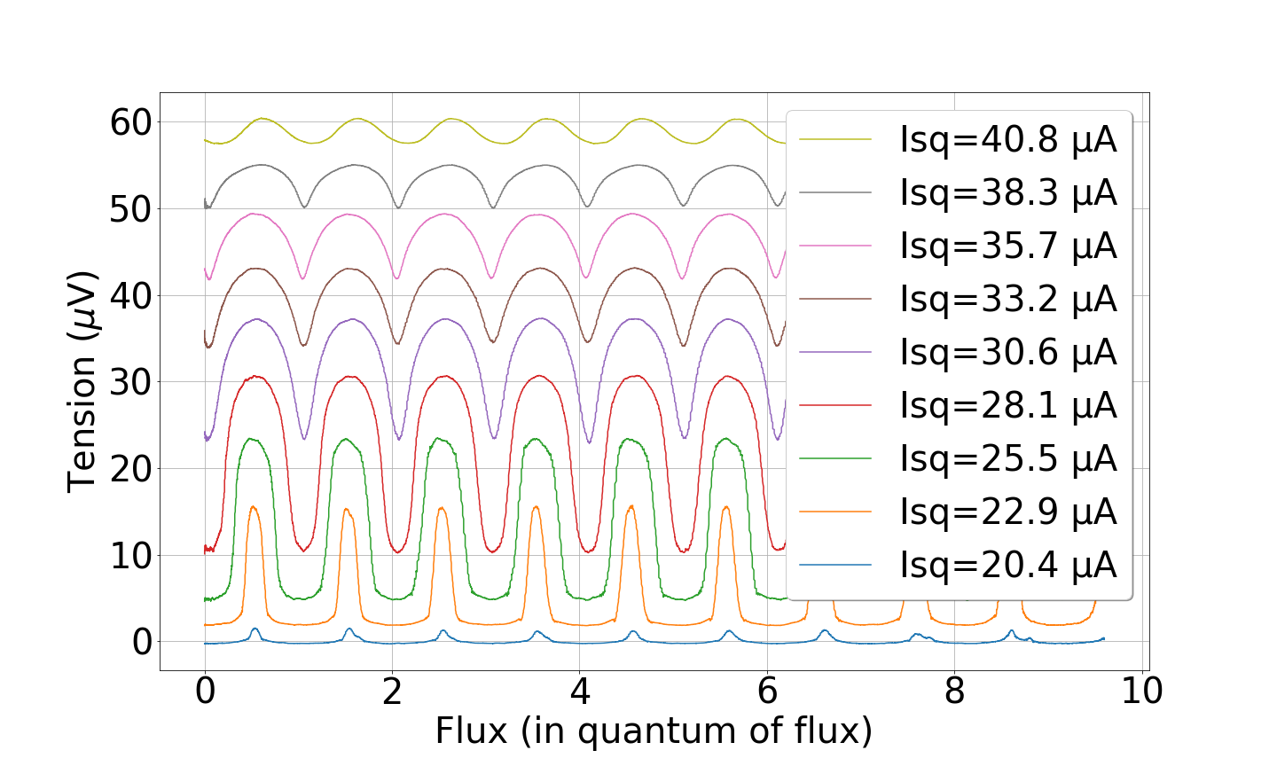
As the SQUID current increases, the amplitude of the response of the SQUID also increases until it reaches a maximum and then it decreases. The optimum corresponds to the maximum amplitude of the SQUID response. Since the same must be supplied to all the SQUIDs per ASIC, it is necessary to select a single bias index for all the SQUIDs for each ASIC. While it seems natural to choose the SQUID current bias corresponding to the majority of the SQUIDs, in reality it does not maximize the number of operational SQUIDs. A SQUID is considered operational if its response is greater than 10 V. The SQUID current is therefore chosen to maximize the number of operational SQUIDs. We also deduced from these data the current noise by dividing the voltage noise (averaged between 40 Hz and 50 Hz) by the slope in the middle of the flux-to-voltage transfer function and by the input coil mutual inductance. Figure 13 shows the histograms of the SQUID response and the deduced current noise for three bias current for the two ASICs.
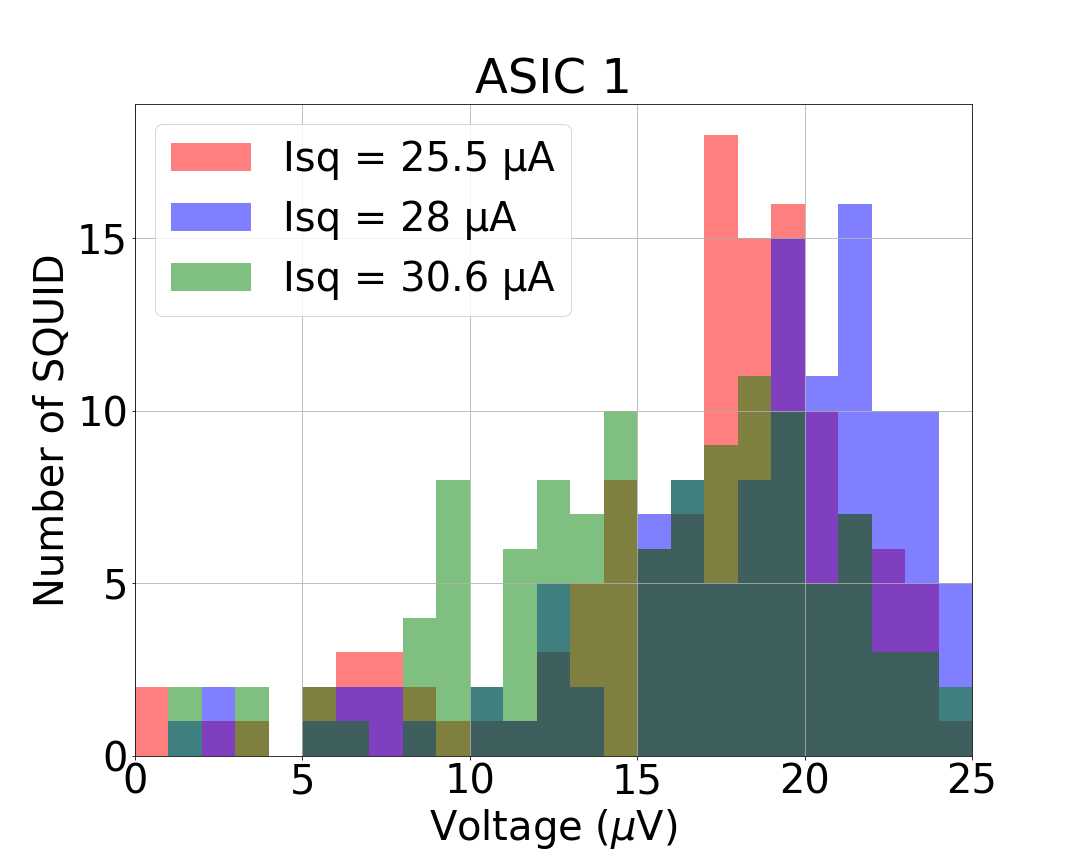
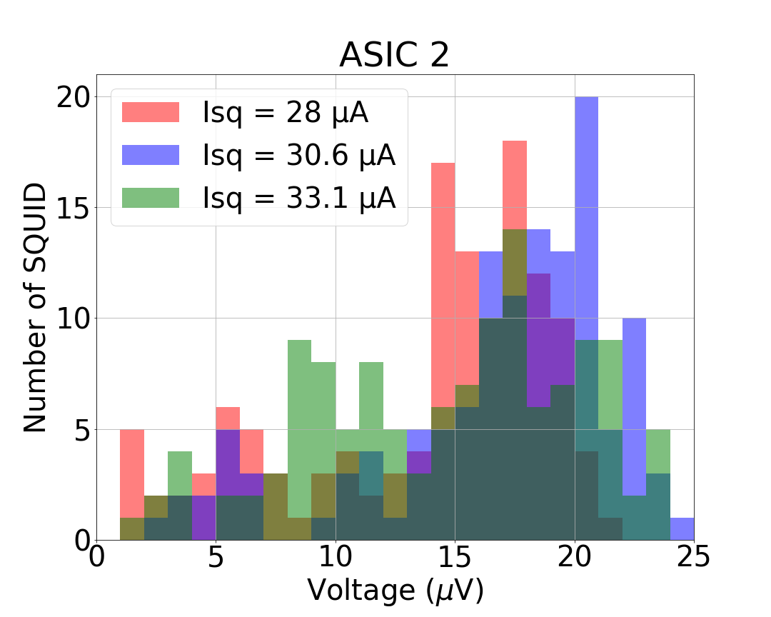
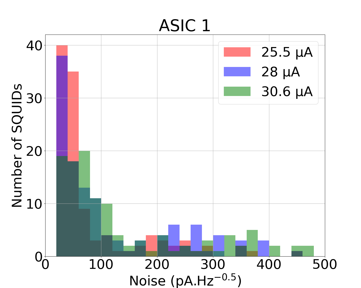
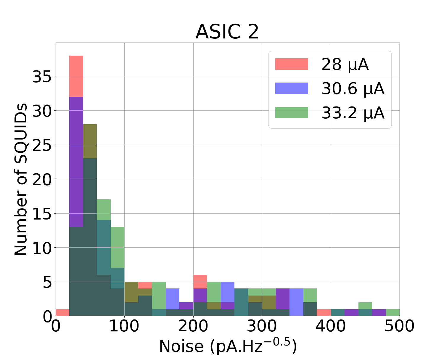
The SQUID voltage swing histograms of Figure 13 show that 28 A is the optimal bias current for ASIC 1 for which 93% of the SQUIDs are operational. For ASIC 2, the histograms give 30.6 A as the best bias current with 91.1% operational SQUIDs. In terms of current noise, the distribution is slightly more peaked for these optimal bias current as shown in the bottom histograms of Figure 13, with a median value around 70 dominated by the TES aliased current noise (see section 4.9).
The yield of SQUIDs for the QUBIC TD is 93% for the 128 SQUIDs connected to ASIC 1, and 89% for the 128 SQUIDs connected to ASIC 2. This corresponds to 119 operational SQUIDs for ASIC 1 and 114 operational SQUIDs for ASIC 2. The total yield is therefore 91%. The optimum bias current is 28.1 A for ASIC 1 and 30.6 A for ASIC 2.
4 TES characterization
The TES array currently used in QUBIC has the reference P87 of the production series. It has been selected after characterizations both at room and cryogenic temperatures. This array has been also fully characterized during the QUBIC calibration phase.
4.1 Selection process and integration
The TES arrays that have been successfully produced undergo visual inspections and resistance measurements at room temperature on a probe station. These measurements are done before integration and wire bonding to detect possible defects or issues with the routing. If successful, the array is integrated in the QUBIC holder and Al wire bonded (Figure 3).
The next steps consist in characterizations at cryogenic temperature. They are done in an Oxford Instrument dilution fridge before integration in the QUBIC cryostat.
4.2 Critical Temperature
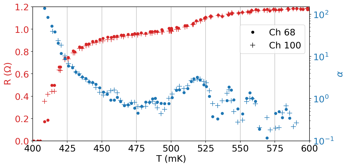
The QUBIC detector wafer includes 8 dark pixels, 4 for each ASIC besides the 124 active ones. These channels consist in NbSi thermal sensors of the same geometry as the ones used on TESs, without thermal decoupling from the silicon wafer. They are located outside the focal plane and are therefore shielded from radiation. Figure 14 shows measurements of the transition from normal to superconducting state for 2 of these dark pixels, measured in a dilution fridge cryostat (which is a dedicated test bed for selection of detectors) by increasing slowly the temperature and with a QUBIC readout chain. The critical temperature is about 412 mK and some temperature dependence is still present above the transition, which allows to still have some sensitivity in case of saturation. The unit-less parameter has been evaluated from these transition curves and is higher than 100 for the lowest part in the transition. A small transition is visible at about 520 mK in this P87 array which is not understood.
4.3 TES normal and parasitic resistances
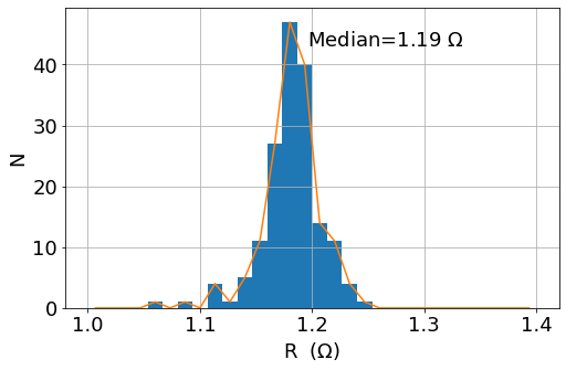
With the bath temperature below the TES critical one, the detectors need to be over-biased (above about 7 V) in order to be in the normal state. A slow and small sine wave voltage oscillation was added in order to deduce the resistance value. Figure 15 top shows the distribution of the normal resistance values for the array P87. It is highly peaked around 1.2 as expected from the transition measurement.
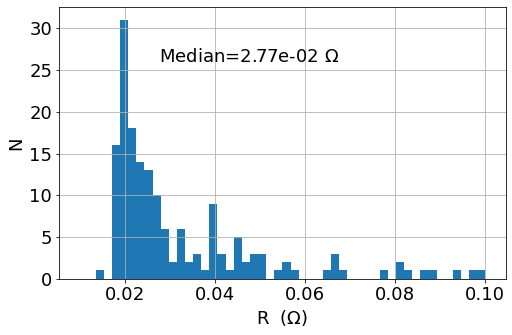
The same procedure is used to determine the resistance in superconducting state, but without any DC bias on the detectors. The residual resistance obtained from these measurements, assuming the TES resistance is 0 , is given by the sum of the shunt resistance (10 m) and the parasitic resistance which is in series with the TES. The parasitic resistance is assumed to come from the connectors used. Figure 15 bottom shows the distribution of these residual resistance values for the array P87. The median is 28 m which leads to a parasitic resistance of about 18 compatible with previous measurements on a dedicated test bench.
4.4 TES parameters
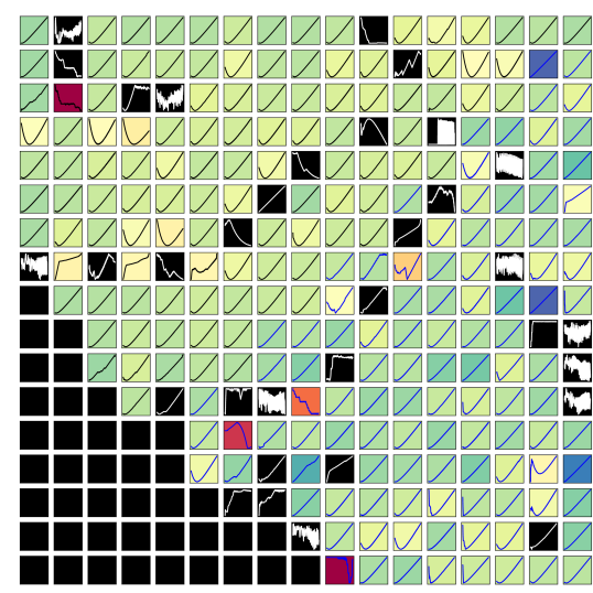
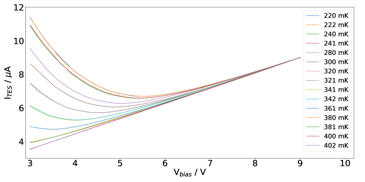
The I-V characteristics at different temperatures have been acquired both in a dilution fridge cryostat and in the QUBIC cryostat with optical window open and closed. The measurement follows the procedure outlined in [9]. Figure 16 shows the I-V curves for the P87 array measured at 360 mK in blind configuration and Figure 17 is an example of the I-V curves for one TES on ASIC2 at different temperatures. The strong Electro-Thermal Feedback (ETF) regime is clearly seen with the increase of the TES current at low bias voltages. An overall yield of about 84% is furthermore obtained in this I-V characterization.
The physical parameters of each TES can be deduced from these measurements. Assuming the TES is in the strong ETF regime and that it is blind, the Power-Temperature relation is classically given by:
| (4.1) |
where is the bias power dissipated in the TES, is the bath temperature, the TES critical temperature, and are constants that depend on the thermal link between the absorber and the bath. In the ETF regime, the bias power is therefore constant for a given bath temperature. The dynamic thermal conductance G is further given by the following equation:
| (4.2) |
Figure 18 shows an example of the Power-Temperature relation for the same TES as in Figure 17. A curve fitting algorithm based on Eq. 4.1 is used to derive the values of , and from measured temperatures and powers.
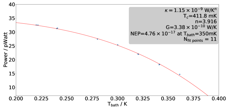
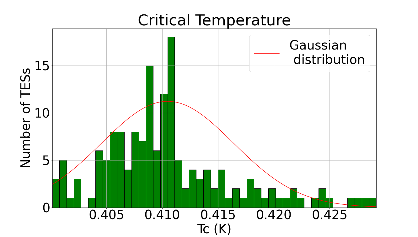
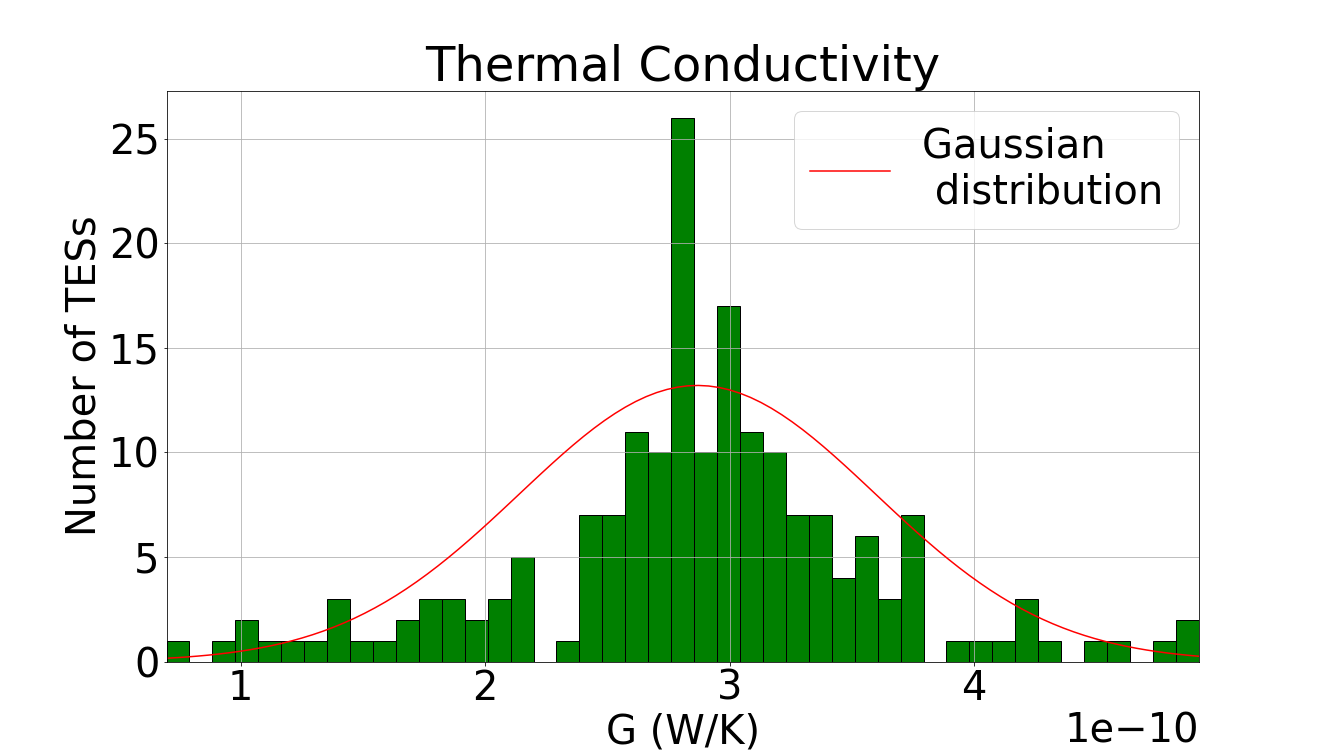
While degenerate with as shown in [3], the index of the power law is around 4 as expected for 500 nm thickness Si3N4 legs. Figure 19 shows the distribution of the critical temperature and dynamic thermal conductance obtained with the fit. The critical temperature is around 410 mK as measured on the dark pixels and the median dynamic thermal conductance is about 300 pW/K. The spread in these parameters is probably inherent to the previously quoted degeneracy between parameters in the fit.
4.5 Detector biasing
A common bias voltage is used for all 128 TESs readout by one ASIC. As seen in Figure 16, there are some inhomogeneity in the pixel behavior, especially below the turnover, which could leads to over or under biasing some pixels. Going deeper in the transition should wipe out this effect since the responsivity depends only on the bias voltage in strong ETF. We nevertheless experienced some instability at low bias due to the fact that the FLL is no more fast enough with respect to TES time constant. The yield therefore decreases when going deeper in the transition. As a consequence, an optimum has to be found between stability and responsivity, which is usually between 2 and 3 V.
4.6 Power background
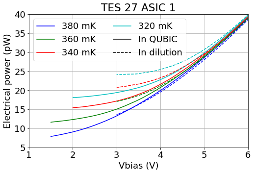
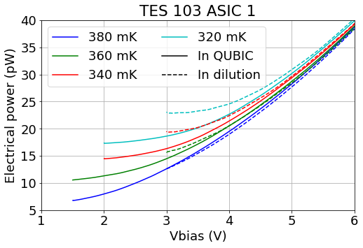
The P-V curves measured during blind characterizations and with the QUBIC optical window open are compared in Figure 20. The comparison leads to an estimate of the power background of the order of a 5 pW which is higher than the expected 1-2 pW from the photometric model of the instrument. This could be due to a difference in temperature sensor calibration between the cryostat used for blind characterizations and QUBIC.
4.7 Phonon Noise Equivalent Power
The expected Phonon Noise Equivalent Power (NEPphonon) was derived from the fitted parameters with the relation [10]:
| (4.3) |
where is the Boltzmann constant, is the bolometer temperature and is a correction coefficient given by:
| (4.4) |
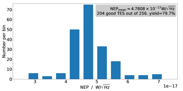
Figure 21 shows histograms of the distribution of the phonon NEP values for the full array derived from the fitted parameters. There is a strong clustering of NEP values around . The dominance of this value in the histogram is an indication of the homogeneity in the fabrication process of the TES array ([11]).
4.8 Time constants
The performances of QUBIC have been tested using a monochromatic calibration source [12] To estimate the time constants, the calibration source is modulated in power with a square wave signal with a frequency of 0.6 Hz and a duty cycle of 33%. The amplitude is chosen to avoid saturation of the detectors while having sufficient signal-to-noise ratio (SNR). The power amplitude on the focal plane is however not constant but corresponds to the synthetic beam. By using a detector located on the calibration source, we checked that the intrinsic rise and fall time is much faster than the expected time constant of the detectors (which is of the order of a few tens of ms).
To process the data, we did a very mild low-pass and high-pass filtering as we do not want the filtering to alter the time constants. We then fold the data for each TES into one period of the calibration source. The filtering and the resulting folded signal is shown in Figure 22 for one TES. The signal peaks on the spectrum can be easily seen.
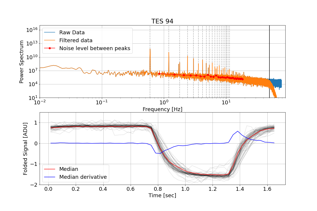
Figure 22 lower shows the normalized (removed average and divided by RMS) folded data for each TES in black, the median is shown in red. The derivative is shown in blue and helps finding the first guess for the start-time of the calibration source shown as a red dot. Note that no selection has been made at this stage to remove TESs with low SNR.
We then fit each TES folded signal (not normalized - meaning with its proper amplitude) with a model for the calibration source signal including a rise time and a fall time.
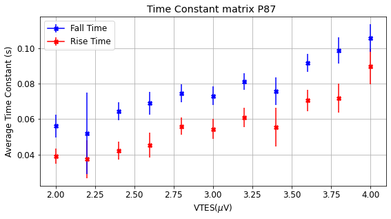
Figure 23 shows the average time constants of all TESs as a function of . The rise time constant appears lower than the fall time indicating again the effect of ETF, but also the fact that we are probably reaching a non-linear regime for most TESs. For small signals, we expect to have a single time constant reaching at most the value of the rise time measured during this sequence, so about 40 ms. This value is enough for QUBIC since the considered scanning speed is about 1 deg/s which leads to a duration of 500 ms for a 30 arcmin beam width.
4.9 Noise characterizations
Aliasing of the TES Johnson noise is a limitation to Time Domain Multiplexing performance. Any source of noise before the SQUIDs with a bandwidth higher than the sampling frequency will be aliased. In Time Domain Multiplexing, the signal of each detector is averaged during the duration of measurement which is smaller than the sampling period by a factor which is the total number of pixels readout in the multiplexing scheme. The noise bandwidth of this averaging is therefore given by . The aliasing leads to an increase of noise given by the square root of the ratio between the noise bandwidth and the Nyquist frequency , that is .
In QUBIC, the ADC frequency drives the multiplexing. The main parameters are therefore: (i) The number of samples to be read out for each TES, and (ii) the total number of pixels to be read out. The maximum number of pixels is equal to which is 128. By reducing the number of pixels sampled, the sampling frequency per pixel is increased. The sampling frequency per TES is . Typical parameters are and leading to and .
The SQUID input inductance value is which leads to a bandwidth higher than 24 kHz for TES resistance above 100 m. For such resistance values, Johnson noise is increased by a factor . To overcome this limitation, a Nyquist inductor can be added in series with the TES. A value of will reduce the noise bandwidth of Johnson noise to 1 kHz for a 100 m resistance giving an increase of noise of 3.6 for the typical parameters. The number of samples can also be reduced in order to increase the sampling frequency and further reduce the aliasing. This limitation in aliasing was expected for the TD and will be improved for the Full Instrument by both adding a Nyquist inductor and increasing the sample rate. The result for the TD is a constraint on NEP of about , which is a factor 2 higher than the FI requirement, but this sensitivity is acceptable for the QUBIC-TD.
4.9.1 Noise in normal and superconducting states
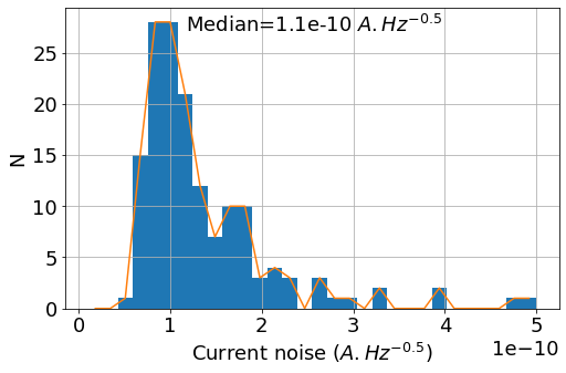
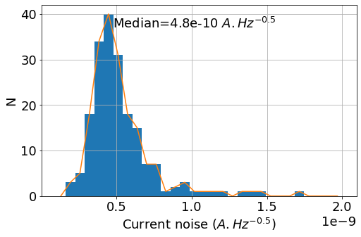
Figure 24 shows the histogram of the measured current noise between 1 Hz and 2 Hz in normal (bias voltage at 8 V) and superconducting state of the TES. In the normal state, a typical value of 110 is obtained, compatible with the expectation within a factor of 2 taking into account the aliasing effect. In the superconducting state, the median current noise is 470 , compatible with the expectation taking into account the aliasing effect and the fact that the shunt resistor and probably part of the parasitic resistance are located on the 1 K stage, which was cooled to only about 2.6 K during this measurement.
4.9.2 Noise in the transition
The detector current noise can be converted into NEP assuming the TES are in strong Electro-Thermal Feedback mode. In this case, the TES responsivity is given by the inverse of the TES voltage, . The TES voltage is obtained from the bias voltage assuming the TES resistance is higher than the shunt resistance: .
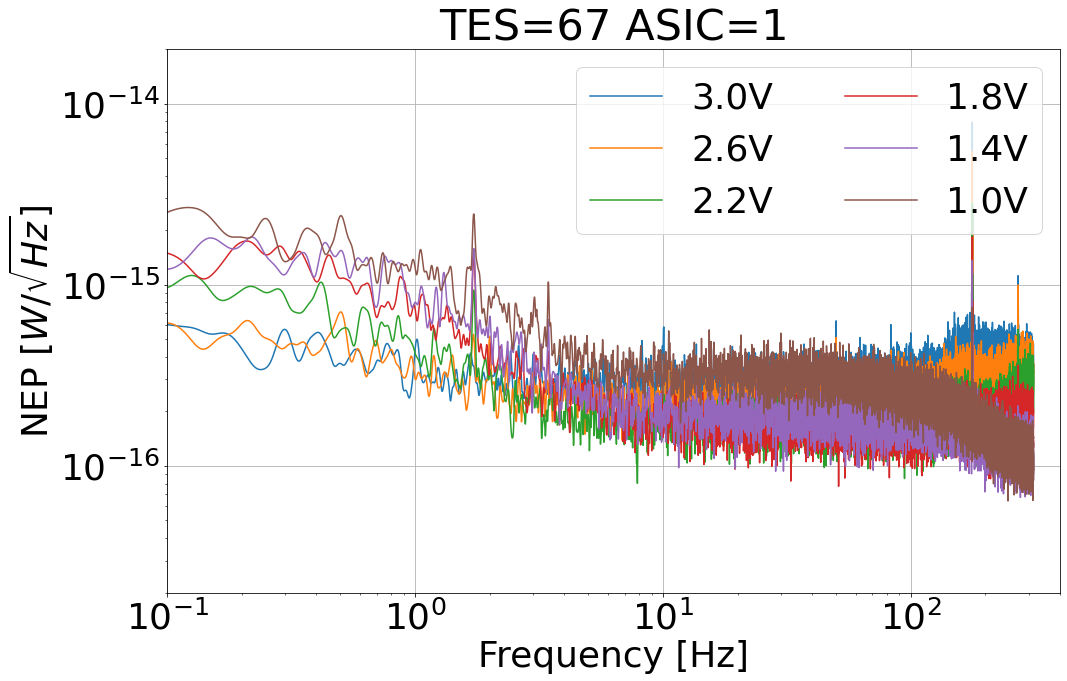
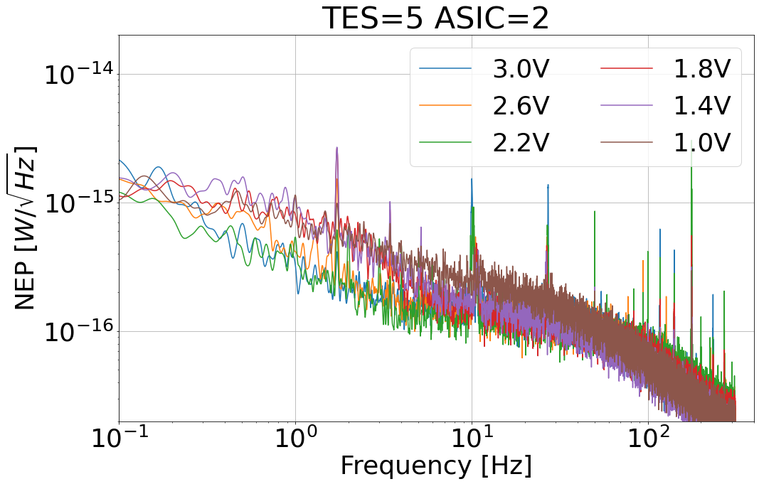
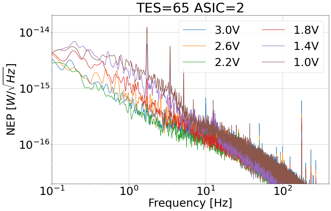
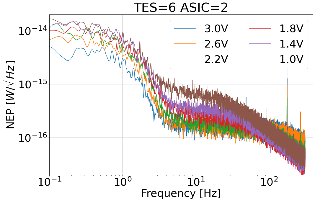
Figure 25 shows some typical NEP spectra at different bias voltages. There is clear evidence of a noise increase at low frequency when decreasing the bias voltage, which is usually produced by the phonon noise in the TES. The noise level is however much higher than expected and it varies between the TES, as seen in Figure 25. This elevated level has further been attributed to a high sensitivity to microphonics from the pulse tubes (PT) as demonstrated in the following.
A test of sensitivity to pulse tube microphonics was carried out by stopping the two units for a few minutes. An example timeline and associated time-frequency analysis is shown in Figure 26. The noise level below few Hz is reduced when both PTs are off while it remains the same at higher frequency. This frequency range where a noise improvement is measured corresponds to the detector bandwidth. The induced parasitic signal is therefore thermal on the detector. The remaining excess of low frequency noise when both PTs are off is attributed to temperature drift.
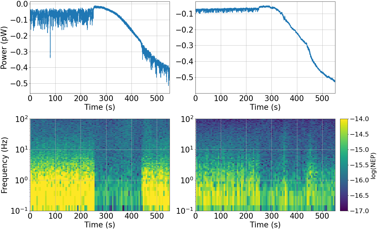
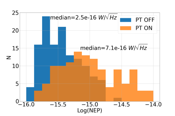
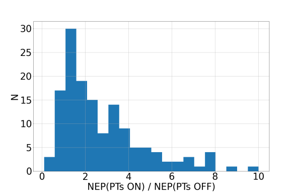
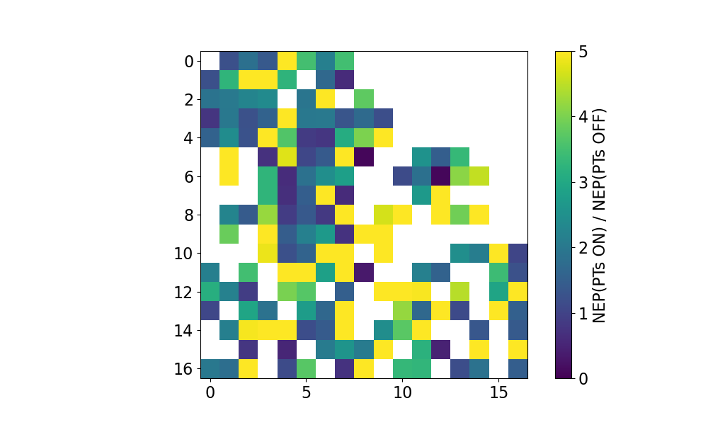
Figure 27 (left) shows the distribution in NEP for two cases: PTs on or off. It appears that the median NEP when the PT are on is about 3 times higher than when they are off. We are clearly dominated by the PT microphonics. The distribution of the NEP ratio between PTs on and off is presented in Figure 27 right and Figure 28 shows the degradation of noise because of the PTs on the TES array. If there are mechanical resonances on the wafer, we expect to measure an increase of excess noise in specific locations and most probably in the middle of the array. It is not clear at this stage if we see here some mechanical specific location on the wafer.
The origin of these perturbations was investigated. We checked from temperature stability measurements that it is not due to thermal fluctuations of the TES or of the 1 K stage. The interpretation is the following: The pulse tube vibrations are exciting mechanical resonance on the TES support structure but also on the TES themselves. This mechanical resonance further dissipates heat on different parts of the system. This assumption is supported by 3 arguments:
-
1.
In the timelines of Figure 26 after the PTs are switched off, we see a small increase in the TES power which is due to a small cooling of the detector, before heating up due to background increase.
-
2.
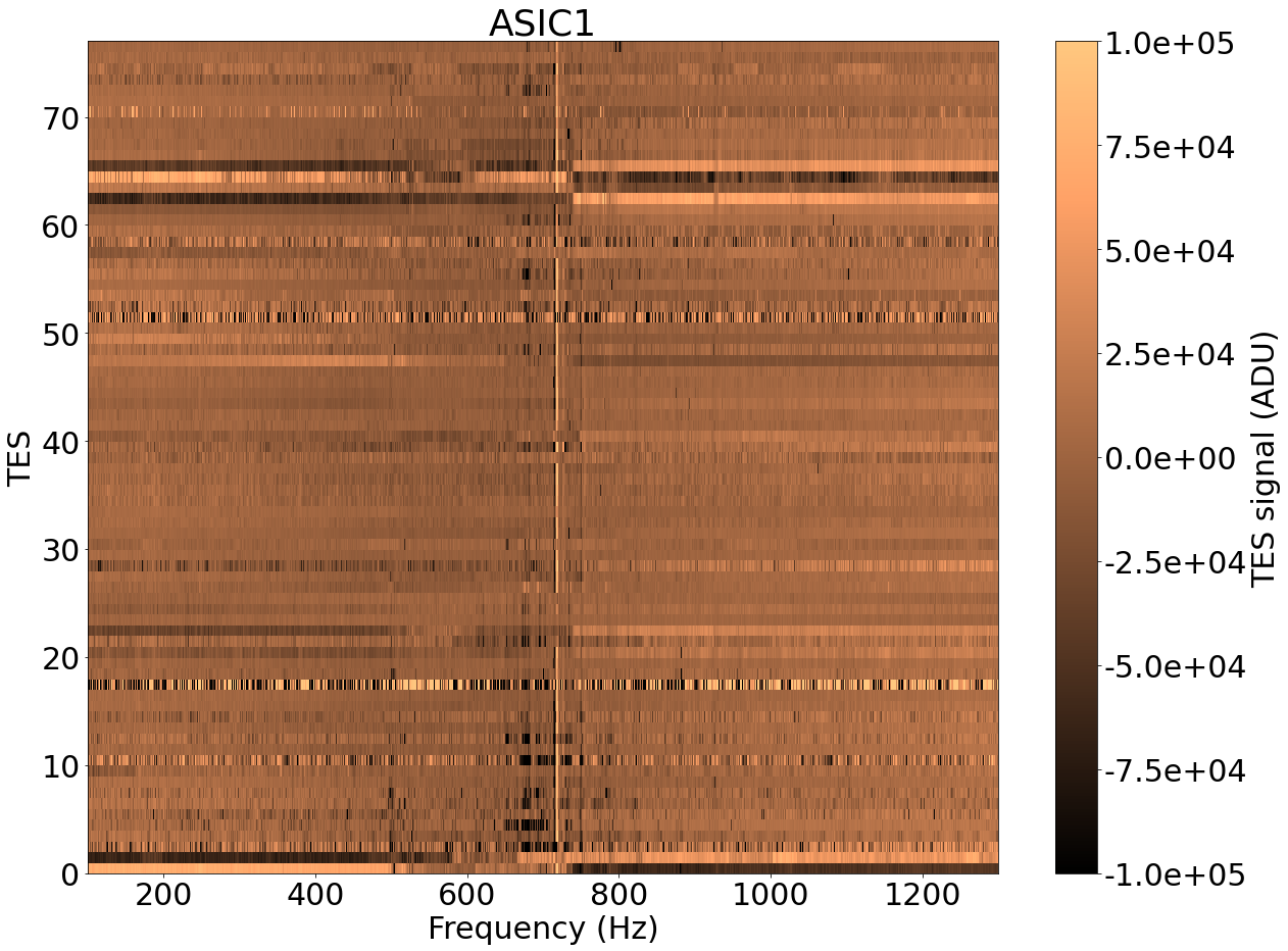
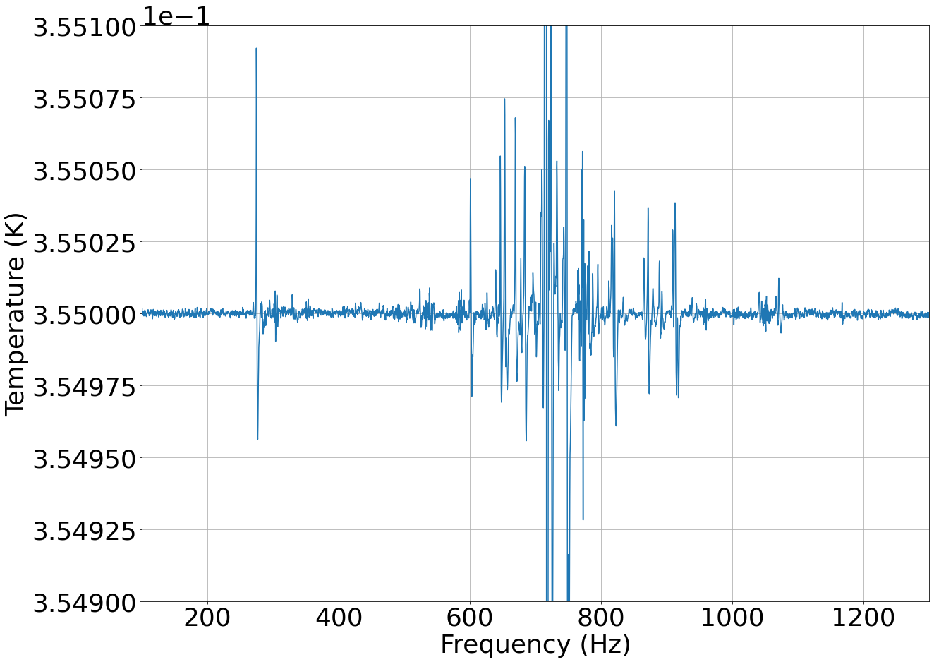
We excited mechanically the cryostat with a speaker connected to an audio amplifier and a sine wave generator sweeping from 100 Hz to 1300 Hz in one hour. Figure 29 shows signals of TES and of the TES stage thermometer as a function of the excited frequency. Resonances are clearly seen, especially around 700 Hz, probably due to a mechanical resonance.
-
3.
With the same setup, we excited the cryostat at a resonance (251 Hz) but the sine wave is modulated in amplitude at 1.5 Hz with 50% depth. Figure 30 shows that this 1.5 Hz is seen directly by the TES. When changing the frequency of resonance (238 Hz for instance), the 1.5 Hz line disappeared from the TES spectra.
We are therefore seeing some heat dissipation produced mainly by the PT vibrations. The environment could also contribute to a lesser extent, for example the traffic on the road nearby.
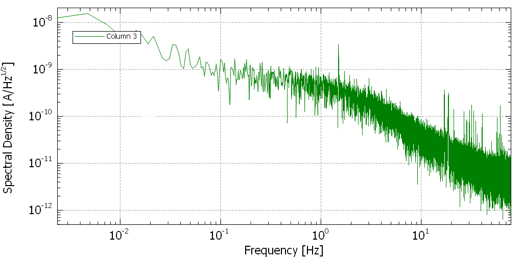
A better mechanical decoupling of the two PTs is needed to overcome this problem. The current thermal straps on the 40 K cold heads are made of thin copper plates which are soft in only one direction. Very soft copper braids will replace these thermal strap to the 40 K shield. The 4 K cold head is already thermally connected to the 4 K shield with very soft copper braids. On the cryostat itself, a soft bellows between the PT and the structure can be added but this needs a detailed study. It should be noted that microphonics is a common problem for PT systems but the effect depends on the detailed mechanical configuration of the setup. This explains why such a strong effect was not seen at the sub-system level. This effect is described by [13, 14, 15], and [16].
5 Conclusion
The QUBIC detection chain based on TES and SQUID, has reached an important milestone. We demonstrated an overall yield of approximately 80 of working detectors (TESs and SQUIDs included), a thermal decoupling compatible with a phonon noise of about at 410 mK critical temperature, and a time constant of about 40 ms which is enough for the instrument. The QUBIC sensitivity is however currently limited to by microphonic noise and aliasing in the readout electronics. The former will be soon improved by mechanically decoupling the first stages of the pulse tubes. The aliasing of the detector noise will be further improved by increasing the sampling frequency and adding Nyquist inductors to reduce the noise bandwidth of the detectors.
Acknowledgments
QUBIC is funded by the following agencies. France: ANR (Agence Nationale de la Recherche) 2012 and 2014, DIM-ACAV (Domaine d’Intérêt Majeur-Astronomie et Conditions d’Apparition de la Vie), CNRS/IN2P3 (Centre national de la recherche scientifique/Institut national de physique nucléaire et de physique des particules), CNRS/INSU (Centre national de la recherche scientifique/Institut national et al de sciences de l’univers). Italy: CNR/PNRA (Consiglio Nazionale delle Ricerche/Programma Nazionale Ricerche in Antartide) until 2016, INFN (Istituto Nazionale di Fisica Nucleare) since 2017. Argentina: MINCyT (Ministerio de Ciencia, Tecnología e Innovación), CNEA (Comisión Nacional de Energía Atómica), CONICET (Consejo Nacional de Investigaciones Científicas y Técnicas).
D. Burke and J.D. Murphy acknowledge funding from the Irish Research Council under the Government of Ireland Postgraduate Scholarship Scheme. D. Gayer and S. Scully acknowledge funding from the National University of Ireland, Maynooth. D. Bennett acknowledges funding from Science Foundation Ireland.
References
- [1] D. Prêle, F. Voisin, C. Beillimaz, S. Chen, M. Piat, A. Goldwurm, and P. Laurent, “SiGe Integrated Circuit Developments for SQUID/TES Readout,” Journal of Low Temperature Physics, vol. 193, pp. 455–461, Nov. 2018.
- [2] M. Piat, B. Bélier, L. Bergé, N. Bleurvacq, C. Chapron, S. Dheilly, L. Dumoulin, M. González, L. Grandsire, J. C. Hamilton, S. Henrot-Versillé, D. T. Hoang, S. Marnieros, W. Marty, L. Montier, E. Olivieri, C. Oriol, C. Perbost, D. Prêle, D. Rambaud, M. Salatino, G. Stankowiak, J. P. Thermeau, S. Torchinsky, F. Voisin, P. Ade, J. G. Alberro, A. Almela, G. Amico, L. H. Arnaldi, D. Auguste, J. Aumont, S. Azzoni, S. Banfi, P. Battaglia, E. S. Battistelli, A. Baùski, L. P. Ferreyro, D. Fracchia, C. Franceschet, M. M. Gamboa Lerena, K. Ganga, B. García, M. E. García Redondo, M. Gaspard, A. Gault, D. Gayer, M. Gervasi, M. Giard, V. Gilles, Y. Giraud-Heraud, M. Gómez Berisso, M. Gradziel, D. Harari, V. Haynes, F. Incardona, E. Jules, J. Kaplan, A. Korotkov, C. Kristukat, L. Lamagna, S. Loucatos, T. Louis, R. Luterstein, B. Maffei, S. Masi, A. Mattei, A. May, M. McCulloch, M. C. Medina, L. Mele, S. Melhuish, A. Mennella, L. Mousset, L. M. Mundo, J. A. Murphy, J. D. Murphy, F. Nati, C. O’Sullivan, A. Paiella, F. Pajot, A. Passerini, H. Pastoriza, A. Pelosi, M. Perciballi, F. Pezzotta, F. Piacentini, L. Piccirillo, G. Pisano, M. Platino, G. Polenta, R. Puddu, P. Ringegni, G. E. Romero, J. M. Salum, A. Schillaci, C. Scóccola, S. Scully, S. Spinelli, M. Stolpovskiy, F. Suarez, A. Tartari, P. Timbie, M. Tomasi, C. Tucker, G. Tucker, S. Vanneste, D. Viganò, N. Vittorio, B. Watson, F. Wicek, M. Zannoni, and A. Zullo, “QUBIC: Using NbSi TESs with a Bolometric Interferometer to Characterize the Polarization of the CMB,” Journal of Low Temperature Physics, vol. 200, pp. 363–373, Apr. 2020.
- [3] M. Salatino, B. Bélier, C. Chapron, D. T. Hoang, S. Maestre, S. Marnieros, W. Marty, L. Montier, M. Piat, D. Prêle, D. Rambaud, J. P. Thermeau, S. A. Torchinsky, S. Henrot-Versillé, F. Voisin, P. Ade, G. Amico, D. Auguste, J. Aumont, S. Banfi, G. Barbarán, P. Battaglia, E. Battistelli, A. Baú, D. Bennett, L. Bergé, J. P. Bernard, M. Bersanelli, M. A. Bigot-Sazy, N. Bleurvacq, J. Bonaparte, J. Bonis, G. Bordier, E. Bréelle, E. Bunn, D. Burke, D. Buzi, A. Buzzelli, F. Cavaliere, P. Chanial, R. Charlassier, F. Columbro, G. Coppi, A. Coppolecchia, F. Couchot, R. D’Agostino, G. D’Alessand ro, P. de Bernardis, G. De Gasperis, M. De Leo, M. De Petris, A. Di Donato, L. Dumoulin, A. Etchegoyen, A. Fasciszewski, C. Franceschet, M. M. Gamboa Lerena, B. García, X. Garrido, M. Gaspard, A. Gault, D. Gayer, M. Gervasi, M. Giard, Y. Giraud-Héraud, M. Gómez Berisso, M. González, M. Gradziel, L. Grandsire, E. Guerrard, J. C. Hamilton, D. Harari, V. Haynes, F. Incardona, E. Jules, J. Kaplan, A. Korotkov, C. Kristukat, L. Lamagna, S. Loucatos, T. Louis, A. Lowitz, V. Lukovic, R. Luterstein, B. Maffei, S. Masi, A. Mattei, A. J. May, M. A. McCulloch, M. C. Medina, L. Mele, S. Melhuish, A. Mennella, L. M. Mundo, J. A. Murphy, J. D. Murphy, C. O’Sullivan, E. Olivieri, A. Paiella, F. Pajot, A. Passerini, H. Pastoriza, A. Pelosi, C. Perbost, O. Perdereau, F. Pezzotta, F. Piacentini, L. Piccirillo, G. Pisano, G. Polenta, R. Puddu, P. Ringegni, G. E. Romero, A. Schillaci, C. G. Scóccola, S. Scully, S. Spinelli, M. Stolpovskiy, F. Suarez, A. Tartari, P. Timbie, M. Tristram, V. Truongcanh, C. Tucker, G. Tucker, S. Vanneste, D. Viganò, N. Vittorio, B. Watson, F. Wicek, M. Zannoni, and A. Zullo, “Performance of NbSi transition-edge sensors readout with a 128 MUX factor for the QUBIC experiment,” in Millimeter, Submillimeter, and Far-Infrared Detectors and Instrumentation for Astronomy IX, vol. 10708 of Society of Photo-Optical Instrumentation Engineers (SPIE) Conference Series, p. 1070845, July 2018.
- [4] S. Marnieros, P. Ade, J. G. Alberro, A. Almela, G. Amico, L. H. Arnaldi, D. Auguste, J. Aumont, S. Azzoni, S. Banfi, P. Battaglia, E. S. Battistelli, A. Baù, B. Bélier, D. Bennett, L. Bergé, J. P. Bernard, M. Bersanelli, M. A. Bigot-Sazy, N. Bleurvacq, J. Bonaparte, J. Bonis, A. Bottani, E. Bunn, D. Burke, D. Buzi, F. Cavaliere, P. Chanial, C. Chapron, R. Charlassier, F. Columbro, A. Coppolecchia, G. D’Alessandro, P. de Bernardis, G. De Gasperis, M. De Leo, M. De Petris, S. Dheilly, L. Dumoulin, A. Etchegoyen, A. Fasciszewski, L. P. Ferreyro, D. Fracchia, C. Franceschet, M. M. Gamboa Lerena, K. Ganga, B. García, M. E. García Redondo, M. Gaspard, D. Gayer, M. Gervasi, M. Giard, V. Gilles, Y. Giraud-Heraud, M. Gómez Berisso, M. González, M. Gradziel, L. Grandsire, J. C. Hamilton, D. Harari, S. Henrot-Versillé, D. T. Hoang, F. Incardona, E. Jules, J. Kaplan, C. Kristukat, L. Lamagna, S. Loucatos, T. Louis, B. Maffei, W. Marty, S. Masi, A. Mattei, A. May, M. McCulloch, L. Mele, S. Melhuish, A. Mennella, L. Montier, L. Mousset, L. M. Mundo, J. A. Murphy, J. D. Murphy, F. Nati, E. Olivieri, C. Oriol, C. O’Sullivan, A. Paiella, F. Pajot, A. Passerini, H. Pastoriza, A. Pelosi, C. Perbost, M. Perciballi, F. Pezzotta, F. Piacentini, M. Piat, L. Piccirillo, G. Pisano, M. Platino, G. Polenta, D. Prêle, R. Puddu, D. Rambaud, P. Ringegni, G. E. Romero, M. Salatino, J. M. Salum, A. Schillaci, C. Scóccola, S. Scully, S. Spinelli, G. Stankowiak, M. Stolpovskiy, A. Tartari, J. P. Thermeau, P. Timbie, M. Tomasi, S. Torchinsky, G. Tucker, C. Tucker, D. Viganò, N. Vittorio, F. Voisin, F. Wicek, M. Zannoni, and A. Zullo, “TES Bolometer Arrays for the QUBIC B-Mode CMB Experiment,” Journal of Low Temperature Physics, vol. 199, pp. 955–961, Jan. 2020.
- [5] D. Prêle, M. Piat, L. Sipile, and F. Voisin, “Operating point and flux jumps of a SQUID in flux-locked loop,” IEEE Transactions on Applied Superconductivity, vol. 26, no. 2, pp. 1–5, 2016.
- [6] D. Prêle, F. Voisin, M. Piat, T. Decourcelle, C. Perbost, C. Chapron, D. Rambaud, S. Maestre, W. Marty, and L. Montier, “A 128 Multiplexing Factor Time-Domain SQUID Multiplexer,” Journal of Low Temperature Physics, vol. 184, pp. 363–368, Jul 2016.
- [7] J. Aumont et al., “QUBIC Technical Design Report,” arXiv e-prints, p. arXiv:1609.04372, Sep 2016.
- [8] D. Prêle, F. Voisin, M. Piat, J. Martino, T. Decourcelle, and C. Chapron, “Capacitively-Coupled SQUID Bias for Time Division Multiplexing,” Journal of Low Temperature Physics, vol. 176, pp. 433–438, Aug. 2014.
- [9] C. Perbost, “TES arrays for the detection of cmb b-mode polarisation : application to the QUBIC experiment,” Archives Ouvertes, Dec 2016.
- [10] J. C. Mather, “Bolometer noise: nonequilibrium theory,” Applied Optics, vol. 21, pp. 1125–1129, Mar. 1982.
- [11] S. Marnieros et al., “TES bolometer arrays for the QUBIC B-mode CMB experiment,” in 18th International Workshop on Low Temperature Detectors, Jul 2019.
- [12] S. A. Torchinsky et al., “QUBIC – III: Laboratory Characterization,” J. Cosmo. Astroparticle Phys., vol. ?, p. ?, Oct 2020. submitted.
- [13] S. R. Dicker et al., MUSTANG: 90 GHz science with the Green Bank Telescope, vol. 7020 of Society of Photo-Optical Instrumentation Engineers (SPIE) Conference Series, p. 702005. 2008.
- [14] C. D. Sheehy et al., The Keck Array: a pulse tube cooled CMB polarimeter, vol. 7741 of Society of Photo-Optical Instrumentation Engineers (SPIE) Conference Series, p. 77411R. 2010.
- [15] R. Maisonobe, J. Billard, M. De Jesus, A. Juillard, D. Misiak, E. Olivieri, S. Sayah, and L. Vagneron, “Vibration decoupling system for massive bolometers in dry cryostats,” Journal of Instrumentation, vol. 13, p. T08009, Aug 2018.
- [16] L. Gottardi, H. van Weers, J. Dercksen, H. Akamatsu, M. P. Bruijn, J. R. Gao, B. Jackson, P. Khosropanah, J. van der Kuur, K. Ravensberg, and M. L. Ridder, “A six-degree-of-freedom micro-vibration acoustic isolator for low-temperature radiation detectors based on superconducting transition-edge sensors,” Review of Scientific Instruments, vol. 90, p. 055107, May 2019.