Large-scale parameterized metasurface design using adjoint optimization
Abstract
Optical metasurfaces are planar arrangements of subwavelength meta-atoms that implement a wide range of transformations on incident light. The design of efficient metasurfaces requires that the responses of and interactions among meta-atoms are accurately modeled. Conventionally, each meta-atom’s response is approximated by that of a meta-atom located in a periodic array. Although this approximation is accurate for metastructures with slowly varying meta-atoms, it does not accurately model the complex interactions among meta-atoms in more rapidly varying metasurfaces. Optimization-based design techniques that rely on full-wave simulations mitigate this problem but thus far have been mostly applied to topology optimization of small metasurfaces. Here, we describe an adjoint-optimization-based design technique that uses parameterized meta-atoms. Our technique has a lower computational cost than topology optimization approaches, enabling the design of large-scale metasurfaces that can be readily fabricated. As proof of concept, we present the design and experimental demonstration of high numerical aperture metalenses with significantly higher efficiencies than their conventionally-designed counterparts.
keywords:
Adjoint technique, Optimization, Metasurface, Metalensumass] Department of Electrical and Computer Engineering, University of Massachusetts Amherst, 151 Holdsworth Way, Amherst, MA 01003, USA \abbreviationsIR,NMR,UV
Introduction
Optical metasurfaces are arrangements of subwavelength meta-atoms that scatter optical waves and generate desirable wavefront, amplitude, and polarization distributions 1. Metasurface-based designs of numerous optical components have been demonstrated, including lenses 2, 3, 4, blazed gratings, 5 and holograms 6, 7, 8, 9. Their planar form factor and the potential for low-cost manufacture have spurred the recent development of complex optical systems made of multiple metasurfaces, or metasystems, such as miniaturized cameras 10, spectrometers 11 and hyper-spectral imaging systems 12. However, cascading multiple metasurfaces quickly increases a system’s optical loss and high-performance metasystems require high-efficiency metasurface components.
Currently, most metasurfaces are designed using a unit-cell-based approach in which each meta-atom is simulated as a part of a periodic array 13, 2, 5, 14. This approach is computationally inexpensive, readily scalable to arbitrarily large structures, and produces designs that can be fabricated easily. However, two implicit assumptions in the unit-cell approach can lead to inefficient metasurface designs: First, the response of a meta-atom with dissimilar neighbors differs from the response of the same meta-atom in an array with identical elements. The ‘local periodicity’ approximation breaks down in structures with rapidly varying meta-atoms, such as high numerical aperture (NA) lenses. This approximation also has reduced accuracy in structures comprising meta-atoms with lower refractive index, in which the response of a meta-atom is more strongly affected by variations of its neighbors 15, 16. Second, the response map used in unit-cell-based methods records only the normally transmitted response for normally incident light. In an actual metasurface, the transmission angle varies, and hence the true response would deviate from the response map 17. These assumptions can lead to significant mismatches between expected and actual responses of a meta-atom in a metasurface. The effect of such mismatch can be seen in reduction of the efficiency of the device, however, it is hard to exactly distinguish the contribution of each assumption without analytical models.
In the absence of simple and accurate models that capture the individual and collective behaviors of meta-atoms, optimization-based design (i.e., inverse design) is a practical alternative. Optical structures have been designed using a variety of optimization-based approaches. A comprehensive review of these methods is presented in ref. 18. Heuristic optimization algorithms based on random explorations of the optimization space (e.g., particle swarm optimization or genetic algorithms) have been used to design diffraction grating filters 19, polarization beam splitters 20 and other small structures. Heuristic optimization is well-suited to problems with a small number of degrees of freedom but inefficient for structures with larger design spaces 21.
In most problems, the gradient of the design objective, necessary for gradient-based algorithms, can be determined using an adjoint technique. Adjoint-based algorithms are suitable for optimization spaces with high dimensionality22, and have been used to design high-performance optical devices, including grating couplers 23, polarization beam splitters24, photonic crystals25, metagratings 24 and metasurfaces26, 27, 26. Adjoint-based optimization is frequently applied to topology optimization problems 28, 23, 24, 25, 26, 27, 29, 22, 30, 29, 31, 32, 33, in which a structure or its meta-atoms are defined by a large number of pixels or sets of curvilinear patterns 22, 30. This can lead to efficient metasurface designs, but because even deeply subwavelength changes in meta-atom geometries can significantly alter the scattering response of a design (see Supplementary Note 1 and Fig. S1), the meta-atom geometries should be accurately approximated during simulations. The accurate representation of meta-atoms with arbitrary shapes require high-resolution meshings, practically limiting the structures to 2D 33, 32, 31, 34, 35 or small 3D 31 designs. As a result, the technique has been mostly used for optimizing periodic structures such as gratings and cylindrical structures 36, 37, 26, 29.
To address this limitation, topology optimization recently has been combined with a local periodicity approximation 32, 29, 34, 35. In this approach, topology optimization is done on small subdomain of the device whose response within the larger structure is approximated by periodic boundary conditions. These subdomains are subsequently stitched together to form the large-scale structure. This approach enables the optimization of large devices; however, subdomains with periodic boundaries do not accurately model the local response in high-NA metalenses or other rapidly-varying structures, limiting the performance of designs arrived at by this approach.
Instead of designing free-form structures, here we propose and demonstrate an adjoint optimization method based on parameterized rectangular meta-atoms (Fig. 1). Parameterized meta-atoms lack the fine features typical of topology-optimized structures , enabling simulations to converge at relatively low resolution and thus very large metasurfaces to be designed. Confining the design space to simple shapes (e.g. rectangular meta-atoms) also reduces the cost of simulation preprocessing steps like subpixel smoothing 38, 39 (Supplementary Note 2 and Supplementary Fig. S2). More importantly, limiting the optimization to this specific subspace of structures (i.e., rectangular meta-atoms) removes a large number of potential local optima traps without significantly affecting device performance and produces designs that conform to a well-established metasurface platform that can be easily fabricated. Our method also relies on a field interpolation technique for and (see methods) and an efficient time to frequency domain conversion technique to reduce the computational cost of simulating large structures. Our method relies on full-wave, finite difference time domain (FDTD) simulations of the entire structure, and iteratively approaches an optimal design via gradient ascent. A similar parameterized approach based on Mie theory was recently proposed by Zhan et. al. 40, 41. However, the approach is limited to spherical meta-atoms, which are challenging to fabricate, and does not account for the substrate’s effect. The adjoint optimization technique does not rely on the two implicit assumptions used in the unit-cell approach, and thereby achieves higher performing designs. First, the variation in coupling among the meta-atoms caused by the rapid variation of their dimensions is accounted for. Second, no assumption is made about angular dependence of the meta-atom scattering response (i.e., its element factor). In the following, we describe our method, and, as proof of concept, use it to design and fabricate two metalenses with 50 m diameter. The focusing efficiencies of metalenses designed using this method show experimental improvements of 24% and 13% for NAs of 0.78 and 0.95 over counterparts designed by the conventional periodic unit-cell method.
Results
Parameterized adjoint design method
We first describe the metastructure design using the parameterized adjoint optimization method. The design process involves finding a set of meta-atom parameters that generate the desired transformation efficiently. As shown in Fig. 2a, to find the optimal design, we optimize the structure iteratively from a trivial initial design (e.g., a uniform array in which all meta-atoms are identical). In each iteration, the gradient of the objective function with respect to all the design parameters is calculated using only two simulations as conceptually shown in Fig. 2b-c. Based on the computed gradient, each meta-atom is updated, generating a new design that is one step closer to the optimal design. This cycle continues until all the parameters converge to their final values (Fig. 2d).
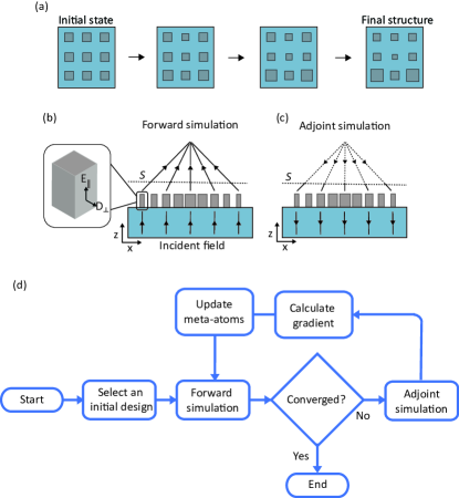
The goal of metastructure design is to transform an incident electric field into a desired transmitted or reflected field distribution . This is schematically illustrated in Fig. 2b, which shows a metasurface transforming a normally incident field into a converging transmitted field. An arbitrary desired output can be achieved by specifying an appropriate transmitted field distribution on a plane above the metasurface. The metasurface we consider consists of an arrangement of dissimilar meta-atoms positioned on a periodic lattice. Each meta-atom’s shape is described by one or more parameters that are variables in the design process. Thus a design can be expressed as a vector containing all the design parameters. In our proposed method, the design is cast as an optimization problem of maximizing the fraction of the output field in the desired field distribution. Specifically, an optimal design maximizes , where
| (1) |
Here is the desired field in the frequency domain on the plane , is the field realized by a design defined by in the forward simulation excited by (Fig. 2b), and * represents the complex conjugate operation. is the complex-valued projection of on .
Optimization starts from an initial design and is updated iteratively via gradient ascent. This process is illustrated in Fig. 2a: after each iteration, approaches its locally optimal value and the performance of the metasurface improves. The gradient is used to determine how changes in the next step and can be computed using an additional simulation called the adjoint simulation. The adjoint simulation uses the same design as the forward simulation, but the structure is instead excited by a surface current density that is placed on the plane which generates a backward propagating wave (see Fig. 2c). The electric field in the adjoint simulation is denoted .
In general, the variation of with respect to small changes in the boundaries of meta-atoms can be found using the functional derivative of . An expression for the functional derivative of based on symmetries of the Green’s tensor can be found in Ref. 42. Here, we consider the special case of rectangular meta-atoms with square cross-sections (inset of Fig. 2b). For such meta-atoms, , where represents the width of meta-atom. Based on the Lorentz reciprocity theorem 43, we show in Supporting Note 3 that the partial derivative of with respect to is given by
| (2) |
where is the angular frequency of the excitation, and are the refractive indices of meta-atom and cladding materials, represents the four side surfaces of the th meta-atom, and are the tangential components of the electric field and normal component of the displacement field obtained in the forward problem, and and are the corresponding fields in the adjoint problem. The gradient of the objective function necessary to determine the next design is given by , where represents the real part of a complex number. Both forward and adjoint simulations are performed using full-wave simulations of the entire metasurface. Although this is computationally more expensive than techniques that employ local periodicity approximations 32, 29, 34, 35, it allows the gradient to be calculated more accurately. The flow diagrams in Fig. 2d and Fig. S3 summarize the optimization procedure.
Metalens design example
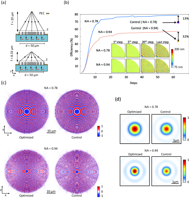
To demonstrate the parameterized adjoint method, we designed two metalenses with NAs of 0.78 and 0.94 (Fig. 3a). The diameters of both metalenses are 50 m, yielding focal lengths of 20 m and 8.3 m.
The metalenses are composed of 430-nm-tall square Si meta-atoms that are arranged on a rectangular lattice with a period of 320 nm. The meta-atoms rest on a fused silica substrate and are surrounded by air. For these designs, the parameter vector consists of the meta-atom widths, , where N19,200 is the number of meta-atoms. By imposing symmetries present in the problem we can reduce the design to 4800 independent variables. Still, the large number of independent variables and the long time required for each simulation precludes a detailed study of the design space. Both metalenses are initialized by a uniform array of 140-nm-wide meta-atoms (i.e., =140 nm).
Both forward and adjoint simulations were performed using a finite difference time domain (FDTD) solver 39 with a sinusoidal excitation that was gradually ramped up. In the forward simulations, the metalenses were illuminated by an -polarized, normally incident plane wave (Fig. 3a) with a free-space wavelength of =850 nm. The desired output field was selected to be the field of an ideal, spherical-aberration-free flat lens (see Methods) 44. To expedite the simulations, symmetric boundary conditions were used along both and axes, reducing the simulation volume by a factor of four. The simulations were run until the results converged, and then the fields were converted from time to frequency domains using the method of ref. 45. The fields on the meta-atom side boundaries, necessary to determine , were interpolated from points on the Yee grid using a bilinear approach (see Methods and Fig. S4). Further simulation details are described in the Methods section.
In each step of the optimization, the design vector was updated according to , where is the step size. The step size was chosen to achieve an average meta-atom width change of a few nanometers. As the optimization proceeded, the step size was manually updated, allowing to converge (see Methods and Fig. S5). To enforce polarization insensitivity, we symmetrized the derivatives along plane (see Methods and Fig. S6).
As a quantitative measure of performance, we calculated the focusing efficiency of each metalens during the optimization process. Focusing efficiency is directly related to the accurate implementation of the desired field profile, and metalenses with higher focusing efficiencies generally have less undesired scattered light and form higher contrast images close to their optical axes. For a fair comparison with the measured values (see the Experimental demonstration section below), we defined the focusing efficiency as the fraction of the power incident on the metalens aperture that passes through a 7-m-diameter aperture in its focal plane. Figure 4b shows the focusing efficiencies of the optimized metalenses as their design evolved during the optimization process. Color-coded meta-atom width maps for these metalenses at several steps during the design process are shown as insets in Fig. 3b. At the first step of the optimization, the metalenses were periodic arrays of posts and had low focusing efficiencies. As the design proceeded, patterns similar to Fresnel zones appeared in the metalenses’ width distributions (Fig. 3b, insets), and their focusing efficiencies increased.
The designs were run for 64 iterations, although after only 25 steps their focusing efficiencies reached plateaus. At the last step, the focusing efficiencies of the optimized metalenses with NAs of 0.78 and 0.94 were 78% and 55%, respectively. For comparison, we designed two control metalenses using the unit-cell approach with NAs, meta-atom heights, lattice constants, and diameters identical to the optimized ones. The simulated focusing efficiencies of the control metalenses are 69% and 43%. The details of the designs and simulations of these control metalenses are presented in Methods. Snapshots of the dominant component of the electric field () at the output apertures of the control and optimized metalenses are presented in Fig. 3c (for distributions see Fig. S7). The field distributions in Fig. 3c show that the optimized metalenses generate the desired fields with smaller phase errors, and consequently produce brighter focal spots than the control metalenses (Fig. 3d). The significantly higher focusing efficiencies of the optimized metalenses compared to their control counterparts demonstrate the efficacy of the parameterized adjoint optimization technique in designing high-performance metasurfaces.
Experimental demonstration
For experimental validation, we fabricated and characterized the optimized and control metalenses. The metalenses were fabricated by depositing a layer of aSi on a fused silica substrate and patterning it using electron beam lithography and dry etching (see Methods for details). Figure 5a shows an SEM image of a fabricated metalens. We characterized the metalenses using a setup schematically shown in Fig. 4b. Metalenses were illuminated by a collimated laser beam with a wavelength of =850 nm. The light transmitted through the metalens was collected by an objective lens with an NA of 0.95 and reimaged by a tube lens on an image sensor. Images of the focal spots, shown in Fig. 5b, show enhanced peak intensities for the optimized metalenses compared to the control ones.
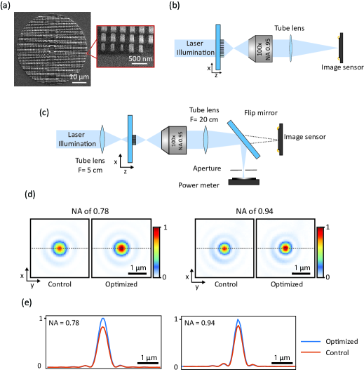
We measured the focusing efficiencies of the metalenses by measuring the ratio of the optical power focused into a 7-m-diameter pinhole in the focal plane of the metalenses and the power incident on their apertures (Fig. 5c). The measured focusing efficiencies of the optimized metalenses with NAs of 0.78 and 0.94 are 65% and 49%, respectively, higher than values of 52% and 43% obtained for their control counterparts. This represents 24% and 13% relative enhancements for the 0.78 and 0.94 NA lenses, respectively. The smaller increase for the higher NA metalens is attributable to the limitations of our measurement setup (the objective lens used has an NA of 0.95) and to its higher sensitivities to fabrication errors.
To study the sensitivity of our designs, an array of metalenses with a range of constant meta-atom offsets were fabricated alongside those characterized in Fig. 4. The study shows that the optimized metalenses have approximately the same sensitivities as the control ones (see Fig. S8).
Discussion
The parameterized adjoint optimization method accurately estimates shape derivatives of parameterized meta-atoms (see Supplementary Note 5 and Fig. S9). In contrast with methods that simulate structures in a dielectric continuum and then discretize to obtain a physically realizable design 22, 46, 26, 47, meta-atoms designed by our method maintain a dielectric discontinuity at their boundaries throughout the whole design process, i.e., the simulation and design domains are the same. Techniques such as level-set representation can also be used to maintain boundaries with a dielectric discontinuity. We previously demonstrated such a technique in a similar silicon on glass material platform 48. Compared to the parametrized technique presented in this article, the simulations for the free-form level-set technique require significantly higher resolutions (i.e., much smaller grid size) to converge and the optimization domain has many more local optima. Due to their small features, the optimized metasurfaces obtained using this level-set approach are also significantly more difficult to fabricate. As a result, the application of level-set representation has been limited to small structures48.
The parameterized adjoint optimization technique can be easily adapted for designing other types of metasurfaces such as achromatic metasurfaces (see Supplementary Note 4). We have presented the design of achromatic metalenses with parameterized shapes in Figs. S10 and S11. These metasurfaces provide comparable efficiencies to the ones designed using topology optimization 31, and do not pose fabrication challenges similar to those of free-form structures.
Using simple, parameterized shapes reduces the dimensionality of the metasurface design space and simplifies the fabrication process. Designs produced by adjoint topology optimization typically require hundreds of steps to converge 26, 22. Parametrization enables us to include our knowledge about principles of operation of metasurfaces by selecting proper arrangement of the meta-atoms and other parameters such as meta-atom height and lattice constant. Our initial design ( uniform metasurface comprising identical meta-atoms) although very simple, includes many important characteristics of the final design, so it can converge faster. The metalenses presented in this work evolved to designs with performance superior to the conventionally-designed controls in fewer than 15 steps. The quick convergence enabled us to optimize large-scale (50 m diameter) metastructures, which, to the best of our knowledge, are currently some of the largest 3D adjoint-optimized metalenses. We previously demonstrated multifunctional multi-layer metasurface ref. 49 devices using similar methods in approximately the same number of iterations. Furthermore, the number of iterations could be further reduced by implementing an adaptive step size 50.
The full-wave simulations employed in this work are computationally expensive. We employed several techniques to keep the optimization of large devices feasible. The computational cost of FDTD simulation is directly related to the grid size used. We employed bi-linear field interpolation, which increases the accuracy of the derivatives without reducing the grid size, keeping the computation time for each iteration tenable. To convert the time-domain fields to the frequency domain, we only used two time samples using an efficient harmonic detection method 45. This technique enables multi-wavelength optimization at minimal additional cost (see Supplementary Note 4): wavelengths with independent objective functions can be incorporated into the simulations by adding appropriate sources and acquiring a few additional time-domain samples without increasing the number or duration of the simulations. Though in this work we presented metalenses optimized from a trivial initial state, we could have selected a conventionally designed metasurface (based on a unit-cell approach) as a starting point, which might have positioned the initial and final designs nearer to each other.
Like any other gradient-based optimization method, designs determined by our method represent local optima. However, parameterization allows us to restrict our search to a judiciously selected subspace by using prior knowledge about the problem. For example, information from low NA conventional designs can be useful in determining the appropriate meta-atom height and the lattice constant for a high NA adjoint-optimized design. To improve the chance of finding the global optimum, multiple optimizations starting from initial designs can be run in parallel. Results of such a multiple-seed optimization are shown in Fig. S12. Despite their different starting points, all designs converged to metalenses with similar focusing efficiencies. The observed behavior might not be general, but it seems to be valid at least for optimizing single layer structures with significant practical impact.
Because our method requires little knowledge about the final structure, it allows us to design elements for which conventional techniques fail to produce efficient designs, like multifunctional metasurfaces 49, 51, 52, 53. In multifunctional devices, the interdependence of parameters is significantly more complex than in single function designs and simple models are unable to model meta-atom behavior accurately. In contrast, our method considers all the complex interactions and generates more efficient designs. Our method is also can be easily extended to other kinds of multi-objective optimizations, like robust designs, that are tolerant to fabrication 54 error.
We envision that the adaptation of the parameterized adjoint optimization to design of large-scale metasurfaces will enable efficient cascading of multiple metasurfaces to implement compact, complex metasystems with high performance.
This work was funded by the Samsung Advanced Institute of Technology, and performed in part at the Center for Nanoscale Systems (CNS) at Harvard University, a member of the National Nanotechnology Coordinated Infrastructure Network (NNCI), which is supported by the National Science Foundation under NSF award no. 1541959.
Methods
Metalens optimization
The two metalenses designed by the adjoint technique and the control metalenses are composed of 430-nm-tall square cross-section aSi meta-atoms () that are positioned on a square lattice with a lattice constant of nm. The meta-atoms are on a fused silica substrate () and are cladded above by vacuum. One quadrant of each of the metalenses are shown in Fig. S7.
The optimization flowchart is shown in Fig. S3. To reduce the required computational resources, we simulated the fields in a small volume (52 m 52 m 1.33 m) around the metasurface. All metalens optimization simulations were performed using a freely-available, open-source FDTD solver 39. Time-domain simulations were run until the fields converged (133 fs). The structure is terminated on all sides by a PML boundary condition. Because only the near field of the structure was simulated, fields at the focal plane (Fig. 4) were obtained by Fourier domain propagation. To further expedite the simulations, we exploited symmetries of the structure and fields: even mirror symmetry was specified along the -axis and odd mirror symmetry along the -axis, reducing the simulated volume by a factor of four.
Simulations were done using a workstation with an Intel E5-2680 CPU; 10 cores were used for each simulation. The FDTD grid size and the step size were adjusted manually when a reduction in the rate of improvement was observed. The simulations in each optimization run began with a grid size of 33 nm (low resolution); after the device efficiency increased, the grid size was reduced to 20 nm (high resolution). Each iteration, consisting of both forward and adjoint simulations, took 15 min at low resolution and 97 min at high resolution. Color-coded plots of meta-atom widths of the optimized and control lens are shown in Fig. S13.
Target field distribution
For an -polarized plane wave input at wavelength originating in a medium with refractive index , the desired field distribution for an ideal metalens with focal length is:
| (3) | ||||
| (4) |
where , 44 is the local deflection angle of the metasurface, and (see Fig. S14).
Field interpolation
The FDTD solver calculates fields on a rectangular grid (Yee grid). However, to determine the gradient, fields on the meta-atom boundaries are required. From the boundary conditions, we know the fields and are continuous. To obtain the boundary fields, we interpolated along axes normal to meta-atom boundaries using a two-sided linear fit approach that considers field values at four Yee lattice points (Fig. S4). For each field component , one linear fit was determined using two points inside the meta-atom, and another, , using two points outside the meta-atom. The field at the boundary () was found based on the distance-weighted average of these two extrapolated values as
| (5) |
where and are given by
Gradient symmetrization and scaling
To obtain polarization-insensitive metalens designs, in addition to the mirror symmetries along and axes described above for the simulation domain, we imposed a symmetry along the line (see Fig. S6). The gradients were first determined for the simulated, -polarized field for a quarter of the metalens and then symmetrized according to:
| (6) |
This operation is equivalent to computing the gradient for circularly polarized input light and optimizing the metalens using this symmetrized gradient ensures its polarization insensitivity. After determining the symmetrized gradient, the step size was selected such that the average of the absolute change of the meta-atom widths was equal to a few nanometers (see Fig. S5). The maximum change in the post widths was limited to 10 times the average value to ensure the first order gradient approximation is valid.
At the beginning of the optimization the absolute value of the average change was selected to be equal to 2 nm. Then, as the reduction in the rate of improvement was observed (see Fig. S5), it was reduced to 0.1 nm.
Control metalens designs
To compare the effectiveness of the proposed design method with the conventional unit-cell design approach, we designed two control metalenses using the unit-cell approach. The control metalenses have the same design parameters as the optimized ones, i.e., with lattice constants of 320 nm, and square cross-section aSi meta-atoms () that are 430 nm tall. Simulated transmittance and phase of the transmission coefficient for a periodic array of meta-atoms are shown in Fig. S15a and were used to obtain the design map shown in Fig. S15b.
Fabrication
All metalenses were fabricated on the same fused silica substrate. To compensate for systematic errors in lithography, etching and other fabrication processes, an array of offsetted designs were included in the pattern. In each element of this array, widths of square meta-atoms are uniformly changed by a value in a range of 15 nm to 45 nm in steps of 5 nm. Figure S8 shows the measured efficiencies of fabricated metalenses with different offset values.
To pattern the metasurfaces, a 430-nm-thick layer of aSi was deposited on the substrate using plasma-enhanced chemical vapor deposition. Then, an approximately 220-nm-thick layer of electron-beam resist (ZEP520A-7, Zeon) was spin coated on the substrate. To avoid charging effects, a conductive polymer layer (ARPC-5090, Allresist) was spin coated on top of the resist. The patterns were defined using a 125 kV electron-beam lithography system (ELS-F125, Elionix), and then an aluminum oxide hard mask was deposited using an electron-beam evaporator. After lifting off the hard mask in a solvent (Remover PG, Microchem), the sample was etched using an inductively-coupled plasma reactive ion etching tool in an SF6/C4F8 gas mixture. The hard mask was removed in a heated solution of ammonium hydroxide and hydrogen peroxide.
Characterization
We used the setup schematically drawn in Fig. S16a to acquire the focusing efficiency of the metalenses. Each metalens was illuminated by a weakly diverging Gaussian beam with a wavelength of 850 nm that was partially focused by a lens with 5 cm focal length (AC254-050, Thorlabs). The light passed through the metalens and came into focus at a focal plane. Light in the focal plane was collected by a microscope objective with an NA of 0.95 (UMPlanFI 100, Olympus), and reimaged by a tube lens (AC254-200, Thorlabs) and a camera (CoolSnap K4, Photometrics).
The focusing efficiency was defined as the ratio of the power focused inside a 7-m-diameter pinhole in the focal plane of the metalens to the total power incident on the metalens. To measure the efficiency, we measured the power in the reimaged focal plane passing through an aperture with a diameter equivalent to a 7-m-diameter pinhole in the metalens focal plane. A flip mirror in the imaging system (dashed box in Fig. S16) allowed us to direct the reimaged spot toward an apertured power meter (S120C, Thorlabs) and measure the focusing efficiencies.
The total incident power is measured by redirecting all the power in the partially focused beam (Fig. S16b) to the power-meter. Power incident on the metalens is different from the the measured power because of the reflection at the second interface of fused silica to air (Fig. S16b). The measured power was corrected to indicate the actual power incident on the lens.
References
- Kamali et al. 2018 Kamali, S. M.; Arbabi, E.; Arbabi, A.; Faraon, A. A review of dielectric optical metasurfaces for wavefront control. Nanophotonics 2018, 7, 1041–1068
- Chen and Craighead 1996 Chen, F. T.; Craighead, H. G. Diffractive lens fabricated with mostly zeroth-order gratings. Opt. Lett. 1996, 21, 177
- Arbabi et al. 2015 Arbabi, A.; Horie, Y.; Bagheri, M.; Faraon, A. Dielectric metasurfaces for complete control of phase and polarization with subwavelength spatial resolution and high transmission. Nat. Nanotechnol. 2015, 10, 937–943
- Chen et al. 2012 Chen, X.; Huang, L.; Mühlenbernd, H.; Li, G.; Bai, B.; Tan, Q.; Jin, G.; Qiu, C.-W.; Zhang, S.; Zentgraf, T. Dual-polarity plasmonic metalens for visible light. Nat. Commun. 2012, 3, 1198
- Lalanne et al. 1998 Lalanne, P.; Astilean, S.; Chavel, P.; Cambril, E.; Launois, H. Blazed binary subwavelength gratings with efficiencies larger than those of conventional échelette gratings. Opt. Lett. 1998, 23, 1081–1083
- Huang et al. 2013 Huang, L.; Chen, X.; Mühlenbernd, H.; Zhang, H.; Chen, S.; Bai, B.; Tan, Q.; Jin, G.; Cheah, K.-W.; Qiu, C.-W.; Li, J.; Zentgraf, T.; Zhang, S. Three-dimensional optical holography using a plasmonic metasurface. Nat. Commun. 2013, 4, 2808
- Zhang et al. 2016 Zhang, X.; Jin, J.; Wang, Y.; Pu, M.; Li, X.; Zhao, Z.; Gao, P.; Wang, C.; Luo, X. Metasurface-based broadband hologram with high tolerance to fabrication errors. Sci. Rep. 2016, 6, 19856
- Zheng et al. 2015 Zheng, G.; Mühlenbernd, H.; Kenney, M.; Li, G.; Zentgraf, T.; Zhang, S. Metasurface holograms reaching 80% efficiency. Nat. Nanotechnol. 2015, 10, 308–312
- Larouche et al. 2012 Larouche, S.; Tsai, Y.-j.; Tyler, T.; Jokerst, N. M.; Smith, D. R. Infrared metamaterial phase holograms. Nat. Mater. 2012, 11, 450–454
- Arbabi et al. 2016 Arbabi, A.; Arbabi, E.; Kamali, S. M.; Horie, Y.; Han, S.; Faraon, A. Miniature optical planar camera based on a wide-angle metasurface doublet corrected for monochromatic aberrations. Nat. Commun. 2016, 7, 443–803
- Faraji-Dana et al. 2018 Faraji-Dana, M.; Arbabi, E.; Arbabi, A.; Kamali, S. M.; Kwon, H.; Faraon, A. Compact folded metasurface spectrometer. Nat. Commun. 2018, 9, 1–8
- Faraji-Dana et al. 2019 Faraji-Dana, M.; Arbabi, E.; Kwon, H.; Kamali, S. M.; Arbabi, A.; Bartholomew, J. G.; Faraon, A. Hyperspectral imager with folded metasurface optics. ACS Photonics 2019, 6, 2161–2167
- Arbabi et al. 2015 Arbabi, A.; Horie, Y.; Ball, A. J.; Bagheri, M.; Faraon, A. Subwavelength-thick lenses with high numerical apertures and large efficiency based on high-contrast transmitarrays. Nat. Commun. 2015, 6, 7069
- Yu et al. 2011 Yu, N.; Genevet, P.; Kats, M. A.; Aieta, F.; Tetienne, J.-P.; Capasso, F.; Gaburro, Z. Light propagation with phase discontinuities: generalized laws of reflection and refraction. Science 2011, 334, 333–337
- Bayati et al. 2019 Bayati, E.; Zhan, A.; Colburn, S.; Zhelyeznyakov, M. V.; Majumdar, A. Role of refractive index in metalens performance. Appl. Opt. 2019, 58, 1460–1466
- Yang and Fan 2017 Yang, J.; Fan, J. A. Analysis of material selection on dielectric metasurface performance. Opt. Express 2017, 25, 23899–23909
- Torfeh and Arbabi 2020 Torfeh, M.; Arbabi, A. Modeling Metasurfaces Using Discrete-Space Impulse Response Technique. ACS Photonics 2020, 7, 941–950
- Molesky et al. 2018 Molesky, S.; Lin, Z.; Piggott, A. Y.; Jin, W.; Vucković, J.; Rodriguez, A. W. Inverse design in nanophotonics. Nat. Photonics 2018, 12, 659–670
- Shokooh-Saremi and Magnusson 2007 Shokooh-Saremi, M.; Magnusson, R. Particle swarm optimization and its application to the design of diffraction grating filters. Opt. Lett. 2007, 32, 894–896
- Shen et al. 2015 Shen, B.; Wang, P.; Polson, R.; Menon, R. An integrated-nanophotonics polarization beamsplitter with 2.4 2.4 m 2 footprint. Nat. Photonics 2015, 9, 378
- Sigmund 2011 Sigmund, O. On the usefulness of non-gradient approaches in topology optimization. Structural and Multidisciplinary Optimization 2011, 43, 589–596
- Jensen and Sigmund 2011 Jensen, J. S.; Sigmund, O. Topology optimization for nano-photonics. Laser and Photonics Reviews 2011, 5, 308–321
- Niederberger et al. 2014 Niederberger, A. C. R.; Fattal, D. A.; Gauger, N. R.; Fan, S.; Beausoleil, R. G. Sensitivity analysis and optimization of sub-wavelength optical gratings using adjoints. Opt. Express 2014, 22, 12971–12981
- Lalau-Keraly et al. 2013 Lalau-Keraly, C. M.; Bhargava, S.; Miller, O. D.; Yablonovitch, E. Adjoint shape optimization applied to electromagnetic design. Opt. Express 2013, 21, 21693
- Burger et al. 2004 Burger, M.; Osher, S. J.; Yablonovitch, E. Inverse problem techniques for the design of photonic crystals. IEICE T. Electron. 2004, 87, 258–265
- Sell et al. 2017 Sell, D.; Yang, J.; Doshay, S.; Yang, R.; Fan, J. A. Large-angle, multifunctional metagratings based on freeform multimode geometries. Nano Lett. 2017, 17, 3752–3757
- 27 Phan, T.; Sell, D.; Yang, J.; Doshay, S.; Fan, J. A. Metasurface Lenses Based on Topology-Optimized Wavelength-Scale Building Blocks. in Conference on Lasers and Electro-Optics, OSA Technical Digest (Optical Society of America, 2018), paper FF3C.6
- Tsuji et al. 2006 Tsuji, Y.; Hirayama, K.; Nomura, T.; Sato, K.; Nishiwaki, S. Design of optical circuit devices based on topology optimization. IEEE Photonics Technol. Lett. 2006, 18, 850–852
- Lin et al. 2019 Lin, Z.; Liu, V.; Pestourie, R.; Johnson, S. G. Topology optimization of freeform large-area metasurfaces. Opt. Express 2019, 27, 15765–15775
- Yang and Fan 2017 Yang, J.; Fan, J. A. Topology-optimized metasurfaces: impact of initial geometric layout. Opt. Lett. 2017, 42, 3161
- Chung and Miller 2020 Chung, H.; Miller, O. D. High-NA achromatic metalenses by inverse design. Opt. Express 2020, 28, 6945–6965
- Phan et al. 2019 Phan, T.; Sell, D.; Wang, E. W.; Doshay, S.; Edee, K.; Yang, J.; Fan, J. A. High-efficiency, large-area, topology-optimized metasurfaces. Light: Science & Applications 2019, 8, 1–9
- Bayati et al. 2020 Bayati, E.; Pestourie, R.; Colburn, S.; Lin, Z.; Johnson, S. G.; Majumdar, A. Inverse designed metalenses with extended depth of focus. ACS Photonics 2020, 7, 873–878
- Lin and Johnson 2019 Lin, Z.; Johnson, S. G. Overlapping domains for topology optimization of large-area metasurfaces. Opt. express 2019, 27, 32445–32453
- Pérez-Arancibia et al. 2018 Pérez-Arancibia, C.; Pestourie, R.; Johnson, S. G. Sideways adiabaticity: beyond ray optics for slowly varying metasurfaces. Opt. Express 2018, 26, 30202–30230
- Sigmund 2009 Sigmund, O. Manufacturing tolerant topology optimization. Acta. Mech. Sinica. 2009, 25, 227–239
- Wang et al. 2011 Wang, F.; Jensen, J. S.; Sigmund, O. Robust topology optimization of photonic crystal waveguides with tailored dispersion properties. J. Opt. Soc. Am. B 2011, 28, 387–397
- Farjadpour et al. 2006 Farjadpour, A.; Roundy, D.; Rodriguez, A.; Ibanescu, M.; Bermel, P.; Joannopoulos, J.; Johnson, S. G.; Burr, G. Improving accuracy by sub-pixel smoothing in FDTD. Tuning the Optic Response of Photonic Bandgap Structures III. 2006; p 63220G
- Oskooi et al. 2010 Oskooi, A. F.; Roundy, D.; Ibanescu, M.; Bermel, P.; Joannopoulos, J. D.; Johnson, S. G. Meep: A flexible free-software package for electromagnetic simulations by the FDTD method. Comput. Phys. Commun. 2010, 181, 687–702
- Zhan et al. 2018 Zhan, A.; Fryett, T. K.; Colburn, S.; Majumdar, A. Inverse design of optical elements based on arrays of dielectric spheres. Appl. Opt. 2018, 57, 1437–1446
- Zhan et al. 2019 Zhan, A.; Gibson, R.; Whitehead, J.; Smith, E.; Hendrickson, J. R.; Majumdar, A. Controlling three-dimensional optical fields via inverse Mie scattering. Sci. Adv. 2019, 5
- Miller 2012 Miller, O. D. Photonic Design: From Fundamental Solar Cell Physics to Computational Inverse Design. Ph.D. thesis, UC Berkeley, 2012
- Harrington 2001 Harrington, R. F. Time-harmonic electromagnetic fields; IEEE Press, 2001; p 480
- 44 McClung, A.; Mansouree, M.; Samudrala, S.; Arbabi, A. Properties of ideal flat metalenses. in Conference on Lasers and Electro-Optics, OSA Technical Digest (Optical Society of America, 2020), paper FM11R.1.
- Furse 2000 Furse, C. M. Faster than Fourier: Ultra-efficient time-to-frequency-domain conversions for FDTD simulations. IEEE Antenn. Propag. M. 2000, 42, 24–34
- Su et al. 2018 Su, L.; Piggott, A. Y.; Sapra, N. V.; Petykiewicz, J.; Vuckovic, J. Inverse design and demonstration of a compact on-chip narrowband three-channel wavelength demultiplexer. ACS Photonics 2018, 5, 301–305
- Sell et al. 2017 Sell, D.; Yang, J.; Doshay, S.; Fan, J. A. Periodic Dielectric Metasurfaces with High-Efficiency, Multiwavelength Functionalities. Adv. Opt. Mater. 2017, 5, 1700645
- Mansouree and Arbabi 2019 Mansouree, M.; Arbabi, A. Metasurface design using level-set and gradient descent optimization techniques. 2019 International Applied Computational Electromagnetics Society Symposium (ACES). 2019; pp 1–2
- Mansouree et al. 2020 Mansouree, M.; Kwon, H.; Arbabi, E.; McClung, A.; Faraon, A.; Arbabi, A. Multifunctional 2.5D metastructures enabled by adjoint optimization. Optica 2020, 7, 77–84
- 50 Johnson, S. G. The NLopt nonlinear-optimization package. \urlhttp://github.com/stevengj/nlopt
- Arbabi et al. 2016 Arbabi, E.; Arbabi, A.; Kamali, S. M.; Horie, Y.; Faraon, A. Multiwavelength polarization-insensitive lenses based on dielectric metasurfaces with meta-molecules. Optica 2016, 3, 628–633
- Kamali et al. 2017 Kamali, S. M.; Arbabi, E.; Arbabi, A.; Horie, Y.; Faraji-Dana, M.; Faraon, A. Angle-multiplexed metasurfaces: Encoding independent wavefronts in a single metasurface under different illumination angles. Phys. Rev. X 2017, 7, 041056
- Zhou et al. 2018 Zhou, Y.; Kravchenko, I. I.; Wang, H.; Nolen, J. R.; Gu, G.; Valentine, J. Multilayer noninteracting dielectric metasurfaces for multiwavelength metaoptics. Nano Lett. 2018, 18, 7529–7537
- Oskooi et al. 2012 Oskooi, A.; Mutapcic, A.; Noda, S.; Joannopoulos, J. D.; Boyd, S. P.; Johnson, S. G. Robust optimization of adiabatic tapers for coupling to slow-light photonic-crystal waveguides. Opt. Express 2012, 20, 21558–21575