Further author information: (Send correspondence to Benjamin G. Westbrook)
E-mail: bwestbrook@berkeley.edu, Telephone: 1 415 308 6193
del⟨⟩
Detector fabrication development for the LiteBIRD satellite mission
Abstract
LiteBIRD is a JAXA-led strategic Large-Class satellite mission designed to measure the polarization of the cosmic microwave background and cosmic foregrounds from 34 to 448 GHz across the entire sky from L2 in the late 2020’s. The primary focus of the mission is to measure primordially generated B-mode polarization at large angular scales. Beyond its primary scientific objective LiteBIRD will generate a data-set capable of probing a number of scientific inquiries including the sum of neutrino masses. The primary responsibility of United States will be to fabricate the three flight model focal plane units for the mission. The design and fabrication of these focal plane units is driven by heritage from ground based experiments and will include both lenslet-coupled sinuous antenna pixels and horn-coupled orthomode transducer pixels. The experiment will have three optical telescopes called the low frequency telescope, mid frequency telescope, and high frequency telescope each of which covers a portion of the mission’s frequency range. JAXA is responsible for the construction of the low frequency telescope and the European Consortium is responsible for the mid- and high- frequency telescopes. The broad frequency coverage and low optical loading conditions, made possible by the space environment, require development and adaptation of detector technology recently deployed by other cosmic microwave background experiments. This design, fabrication, and characterization will take place at UC Berkeley, NIST, Stanford, and Colorado University, Boulder. We present the current status of the US deliverables to the LiteBIRD mission.
keywords:
SPIE Digital Forum, CMB, Detectors, Space-Mission, Polarization, Inflation, Cosmic Foregrounds, Satellite, LiteBIRD1 Introduction
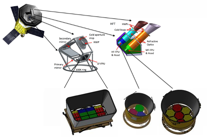
Litebird is a JAXA-led strategic Large-Class satellite mission that will map the the polarization of the Cosmic Microwave Background (CMB) and cosmic foreground over the entire sky with an angular resolution appropriate to cover the multipole range . The payload consists of three telescopes called the Low-Frequency Telescope (LFT), Mid-Frequency Telescope (MFT), High-Frequency Telescope (HFT) each of which has a corresponding Focal Plane Unit (FPU). It is the primary responsibility of the US team to deliver the flight model (FM) FPU s including an Adiabatic Demagnetization Refrigerator (ADR) cooling system for the mission. Litebird will deploy a total of 15 detector bands ranging from 34 to 448 which are distributed across the Low-Frequency Focal Plane Unit (LF-FPU), Mid-Frequency Focal Plane Unit (MF-FPU), and High-Frequency Focal Plane Unit (HF-FPU). The Focal Plane Modules (FPMs) for the LF-FPU and MF-FPU consist of lenslet coupled sinuous antenna Transition-Edge Sensor (TES) bolometer arrays with di- and tri-plexing RF filters. The HF-FPU consists of horn coupled orthomode transducer (OMT) TES bolometer arrays with two dichroic arrays and one monochromatic array. An overview of the Litebird mission can be found in a companion SPIE paper[1] and detailed descriptions of the LFT and the Mid- and High-Frequency Telescopes (MHFT) can be found in two other SPIE companion papers as well [2, 3].
The LF-FPU holds eight square tiles with four distinct pixel types and two distinct FPM types with a pixel pitch of 32 for the lowest frequency pixels and 16 for the higher frequency pixels. The LF-FPU has a frequency coverage of 34 to 148 GHz making it sensitive to both synchrotron radiation and the CMB. The MF-FPU holds 7 hexagonal tiles and 2 different FPM types each with a single pixel type for each, but share a common pixel pitch of 12 . These FPM s cover the frequency range from 90 to 180 and are designed to be most sensitive at CMB frequencies. The HF-FPU holds 3 hexagonal FPM s each with their own pixel type; the two lower frequency FPM s have a pixel pitch of 7 and are dichroic, while the highest frequency FPM has a pixel pitch of 6.1 and is monochromatic. The total bandwidth of this FPM is 200 to 448 and will be sensitive to the dusty cosmic foregrounds.
The stringent scientific requirements of the Litebird mission flow down to challenging technical specifications for the detection chain. In particular, the FPU s must have an unmodulated 1/f-knee 20 in order to measure the largest angular scales of the CMB. The combined sensitivity of the FPU s will be 2.16 K-arcmin with a typical angular resolution of 0.5 at 150 . Full success of the Litebird mission would achieve 0.001, where is the total error on the tensor-to-scalar ratio .
The US team consists of two fabrication sites: the Marvell Nanofabrication Laboratory (MNL) at the University of California, Berkeley (UC Berkeley) and Boulder Microfabrication Facility (BMF) at the National Institute of Standards and Technologies (NIST). Both institutions have extensive heritage in fabricating TES bolometer arrays for studies of the polarization of the CMB for both ground-based and balloon-borne experiments making them especially suitable for Litebird. The MNL is a 10,000 square foot class 100 clean room that has rich heritage of fabricating detectors for CMB experiments including: APEX-SZ, SPT-SZ, EBEX, ASTE-TESCAM, POLARBEAR-1, Simons Array (SA), and Simons Observatory (SO). The BMF is a 18,000 square foot class 100 clean-room that has fabricated detectors for many mm and sub-mm CMB projects including the ACTPol, Advance ACTPol, SPTPol, SPIDER, SO and BLAST. Testing of all of the Low-Frequency (LF), Mid-Frequency (MF), High-Frequency (HF) FPMs will take place at UC Berkeley (LF), University of Colorado, Boulder (CU) (MF), and Stanford University (Stanford) (HF) respectfully. Additional chip and array testing will take place at Kavli Institute for the Physics and Mathematics of the Universe (IPMU), High Energy Accelerator Research Organization in Tsukuba, Japan (KEK), University of Tokyo (U of T) including the validation of other key technological components of Litebird. The entire focal plane will be integrated at UC Berkeley for final characterization prior to flight. In this proceeding, we discuss the current status of the design, fabrication, and testing of these FPUs as part of the US contribution to the Litebird satellite mission.
2 US Deliverables
Litebird requires measurements with 15 frequency bands between 34 and 448 to achieve the total sensitivity of -arcmin with three years of observations. In order to meet this requirement, these 15 bands are distributed throughout three different FPU in three different telescopes with 9 distinct pixel types for the mission (see Table 1 for more details on the Litebird bands). As shown in figure 1, the shapes of the FPU are matched to the illumination patterns of their respective telescopes.
2.1 Focal Plane Units
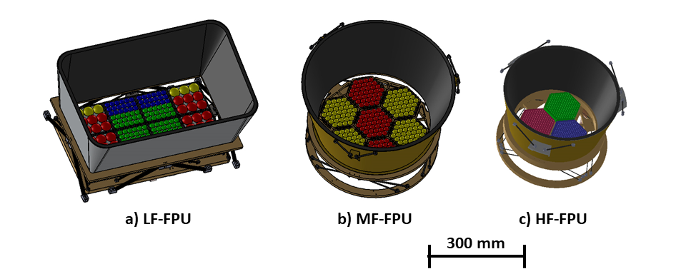
Litebird will deploy a FPU for each of the telescopes, and are named after each telescope respectively: LF-FPU, MF-FPU, and the HF-FPU. The details of the distribution of the mission’s 15 bands and pixel counts in shown in table 1 and CAD diagrams of each FPU is shown in figure 2. The details of each FPU are discussed in sections 2.3, 2.4, and 2.5.
Generally speaking the three FPUs share a common architecture. A Focal Plane Structure (FPS) provides thermal insulation from the Joule-Thomson 5 K (JT5) cooled stage and thermal connection to the Adiabatic Demagnetization Refrigerator that cools the Sub-Kelvin stages (Sub-K ADR) in order to operate an array of individual FPMs at 100 . The telescope designs drive the focal plane layouts; the LFT FPU is rectangular to match the oblong illumination pattern of the crossed Dragone telescope design while the MFT and HFT FPUs are hexagonal arrays which pack the pixels most efficiently into the the axis-symmetric MFT and HFT refractor telescopes.
2.2 Focal Plane Modules
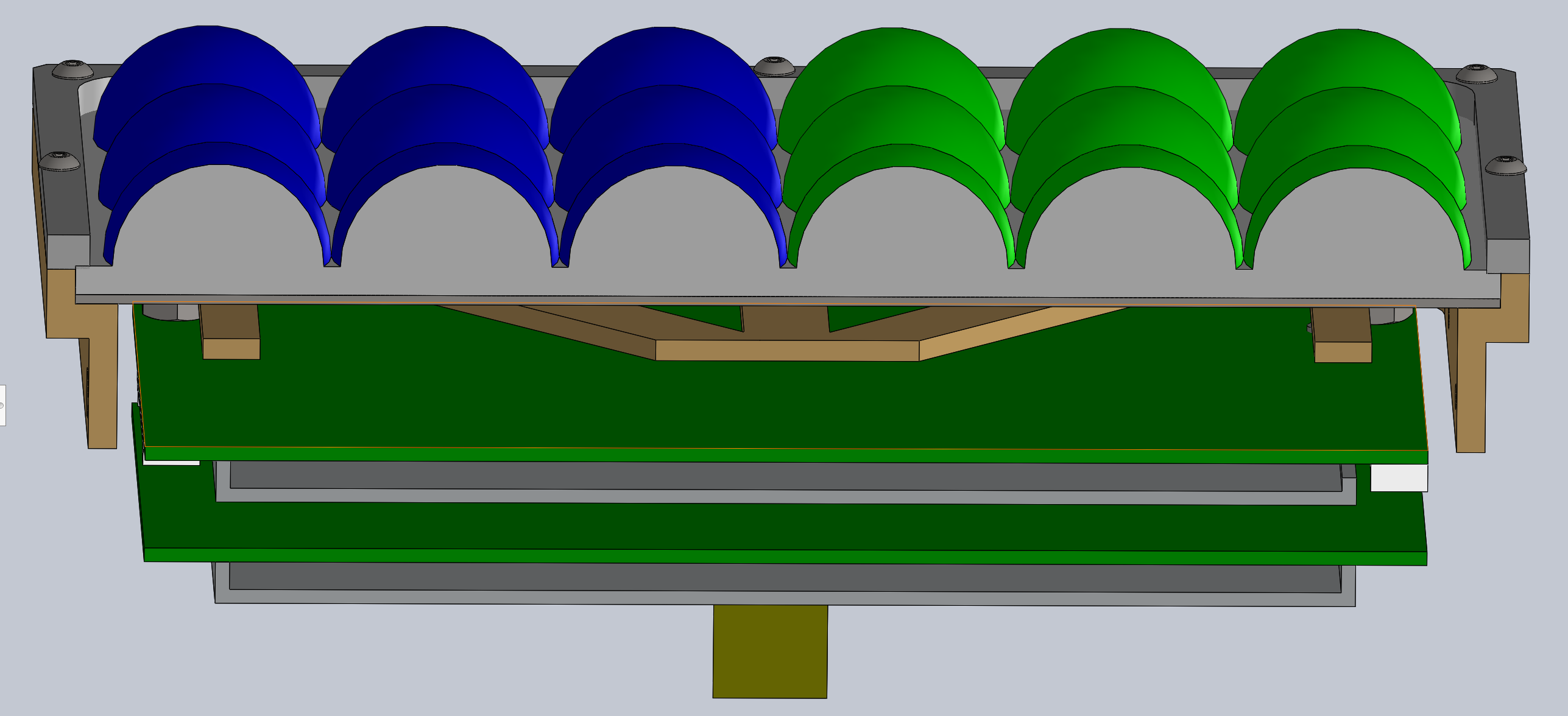
The FPMs of Litebird are filled with arrays of antenna-coupled TES fabricated on silicon wafers coupled to a multiplexed readout system. Each FPM consists of a single detector array, optical coupling hardware (lenslet or horn arrays, backshort wafers, etc.), the Cryogenic Readout Units (CRU), and mechanical structures which hold these parts together and provide an interface to the FPS as shown in figure 3.
2.2.1 Optical Coupling
The electromagnetic coupling structures for each focal plane were chosen based on our analysis of what the most appropriate technology for the specific frequency ranges. The LFT and MFT FPMs share a common architecture of lenslet-coupled sinuous antenna arrays and the HFT FPMs use horn-coupled OMT arrays. Both technologies sense orthogonal polarizations simultaneously and are coupled to on-chip micro-strip bandpass filters which split the signal into one, two, or three frequency bands. The power from each frequency and polarization propagate along superconducting micro-strip lines where it is then dissipated on thermally isolated TES bolometer islands. TES electrical bias lines carry the induced signal to the edge of the silicon wafer where it is wire-bonded to a flexible circuit leading to the cold readout. The TES technology is able to reach the instantaneous sensitivity required by the Litebird mission and is a mature technology with well-established use in ground-based and sub-orbital CMB experiments [4, 5, 6, 7, 8]. Details of each type of optical coupling are shown in figure 4.
| Telescope |
|
FPM |
|
|
|
|
|
|||||||||||||
| LF-1 | 40/60/78 | 34 - 87 (53) | 32 | 12 | 72 | |||||||||||||||
| LF12 | LF-2 | 50/68/89 | 43 - 99 (56) | 32 | 24 | 144 | ||||||||||||||
| LF-3 | 68/89/119 | 60 - 133 (73) | 16 | 72 | 432 | |||||||||||||||
| LFT | Lenslet/ Sinuous | LF34 | LF-4 | 78/100/140 | 69 - 162 (93) | 16 | 72 | 432 | ||||||||||||
| MF1 | MF-1 | 100/140/195 | 77 - 224 (147) | 12 | 183 | 1098 | ||||||||||||||
| MFT | Lenslet/ Sinuous | MF2 | MF-2 | 119/166 | 105 - 216 (111) | 12 | 244 | 976 | ||||||||||||
| HF1 | HF-1 | 195/280 | 166 - 322 (156) | 7 | 127 | 508 | ||||||||||||||
| HF2 | HF-2 | 235/337 | 200 - 388 (188) | 7 | 127 | 508 | ||||||||||||||
| HFT | Horn/ OMT | HF3 | HF-3 | 402 | 366 - 448 (92) | 6.1 | 169 | 338 |
2.2.2 Structure
The FPSs each contain two intermediate temperature stages at 1.8 and 300 between the FPUs at 100 and the 4.8 telescope structures. A free-space low pass edge filter and a Focal Plane Hood (FPH) are supported by the 1.8 stage. Aluminized thin film spans the interstage gaps to block radio frequency and residual warm thermal radiation. The requirements include a thermal budget for each stage and mechanical performance to survive launch loads and keep resonances clear of the science band while in operation. Our current baseline includes aluminum, titanium, and copper metallic parts and carbon fiber reinforced plastic inter-stage support struts. A trade-off study is in progress to determine whether struts can be designed to be able to survive launch loads without launch locks.
2.3 LF-FPU
The LF-FPU has a FOV of 18∘ x 9∘ with a typical beam size of 1 degree. The crossing angle of 90∘ and the F#3.0 were chosen to minimize the effects of stray light, especially at the edges of the FOV. To further mitigate this effect we place the lowest frequency pixels in Litebird which are the yellow pixels in the left hand side of figure 2. The large pixel spacing allows for excellent Lyot efficiency which further optimizes the LF-FPU for the science goals of Litebird.
The LF-FPU has total of eight 140 x 140 square tiles arranged in a rectangular 4x2 array. There are two unique types of FPMs in the LF-FPU that will contain four pixel types called LF-1 (yellow), -2 (red), -3 (blue), and -4 (green). The indexing corresponds with the average frequency of a given pixel type. Table 1 shows the individual specifications for the pixels in these FPMs shown in 2. Three LF-1 (40/60/78 ) and and six LF-2 (50/60/78 ) pixels are distributed on a 9-pixel FPM with a pixel pitch of 32 mm. The LF-1 (i.e. the lowest frequency) pixels are placed at the edges of the LF-FPU to minimize the impacts of scattered light on optical performance. The LF-3 (68/89/119 ) and LF-4 (78/100/140 ) bands are distributed equally in each of four LF FPUs. These FPUs have a pixel pitch of 16 and have 18 LF-3 and 18 LF-4 pixels each. We oriented the FPUs such that the highest average frequency pixels are in the central region of the focal plane.
2.4 MF-FPU
The MFT is an axially symmetric refractor telescope with a FOV of 28 ∘ with F#=2.2 with an aperture stop of 300 . There are 2 unique types of FPMs that will go into the MF-FPU, which we refer to as MF-1 (100/140/195 ), and MF-2 (119/116 ). Both FPMs have a pixel pitch of 12 . There are three MF-1 and four MF-2 modules in the MF-FPU.
2.5 HF-FPU
The design of the HFT is essentially compact version of the HFT; it is also an axially symmetric refractor telescope with a FOV of 28 ∘ with F#=2.2 but has aperture stop of 200 . There are 3 unique types of FPMs that will go into the HF-FPU, which we refer to as HF-1, HF-2. HF-3 all of which are horn-coupled OMT detectors described in section 3.2.1 and have an architecture very similar to that of [6, 8]. The HF-1 and HF-2 are dichroic pixels with band centered on 195/280 and 235/337 respectively. The highest frequency FPM of Litebird HF-3 has monochromatic pixels with bands centered at 402 and a maximum detection frequency of 448 .
3 Detector Design
Litebird will deploy two detector architectures to optimize the overall sensitivity of the experiment as shown in Figure 4. The LFT and MFT will deploy lenslet-coupled sinuous antenna TES bolometer arrays and the HFT will deploy horn-coupled OMT TES bolometer arrays. The details of each detector architecture are shown in figure 4. The arrays are fabricated at the MNL at UC Berkeley and the BMF at NIST. Due to the commonality of many of the RF and bolometric components of the array architectures the fabrication of all of the arrays is quite similar even when comparing the fabrication flow for sinuous antennas and OMTs.
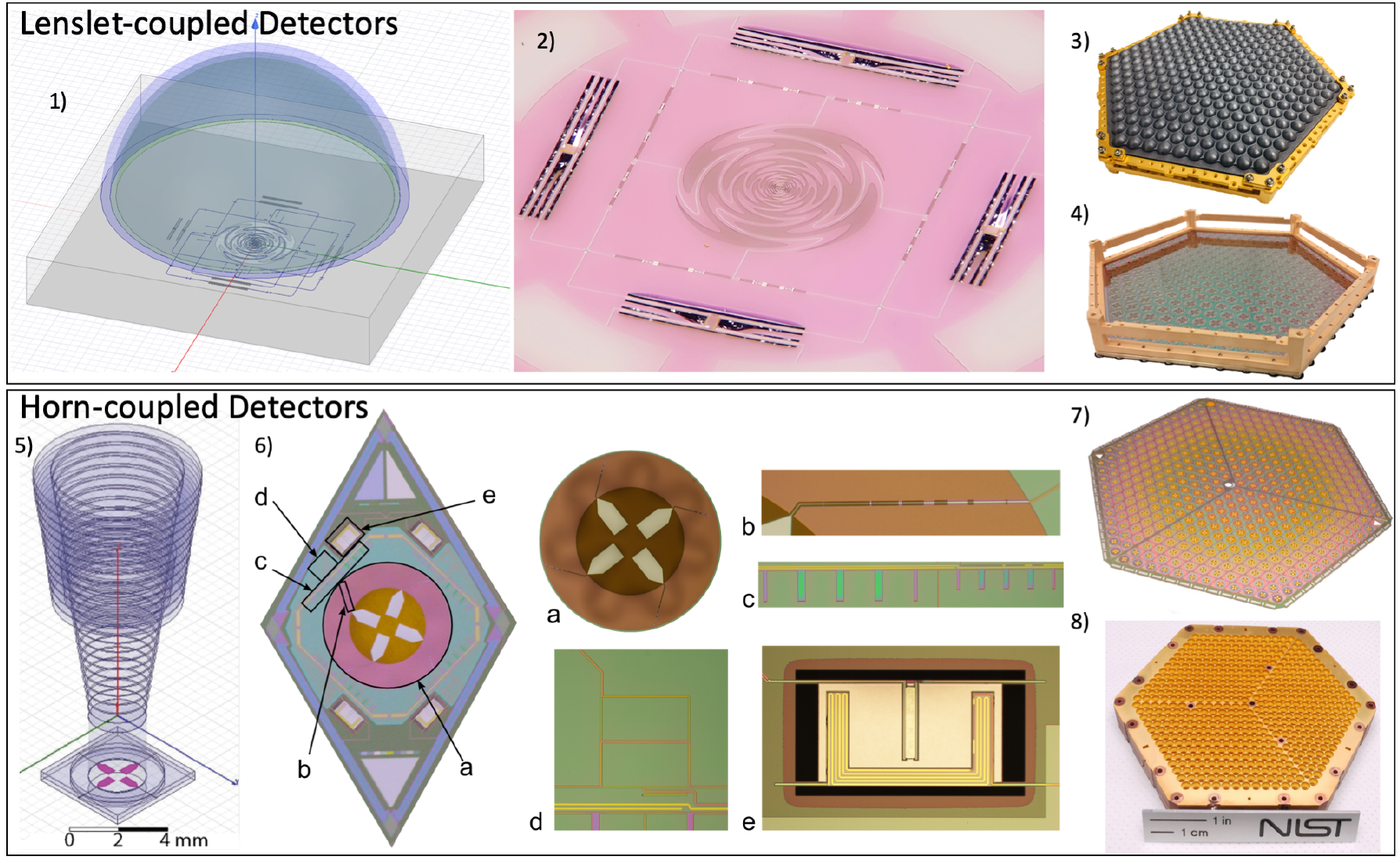
3.1 Lenslet Coupled Sinuous Antenna Arrays
A contact lens placed near a planar antenna increases the forward gain of the antenna and is a technique used in mm and sub-mm astronomy for many years. Panel 1 of figure 4 shows a High Frequency Simulation Software (HFSS) simulation setup of a lenslet placed over a LF-4 pixel. The lenslet coupled double slot dipoles have been deployed by the POLARBEAR [4] to measure E-modes and constrain the sum of neutrino masses. More recently lenslet-coupled sinuous antenna arrays have been deployed by the SA and South Pole Telescope Third Generation (SPT-3G). In the case of SA the detectors are dichroic 90/150 pixels and in the case of SPT-3G the detector arrays are trichoric 90/150/220 detectors [9, 10].
Sinuous antennas are broadband log-peridoc self-similar antennas sensitive to polarization. The log periodic nature of the antenna makes it ideal for the broad frequency coverage required by the Litebird science goals. This technology is being deployed by the SA and SPT-3G and will be deployed by the SO [9, 10, 11]. The broadband nature of these antennas are well suited for the Litebird mission, especially for the LFT and MFT where 11 of the 15 Litebird bands are located.
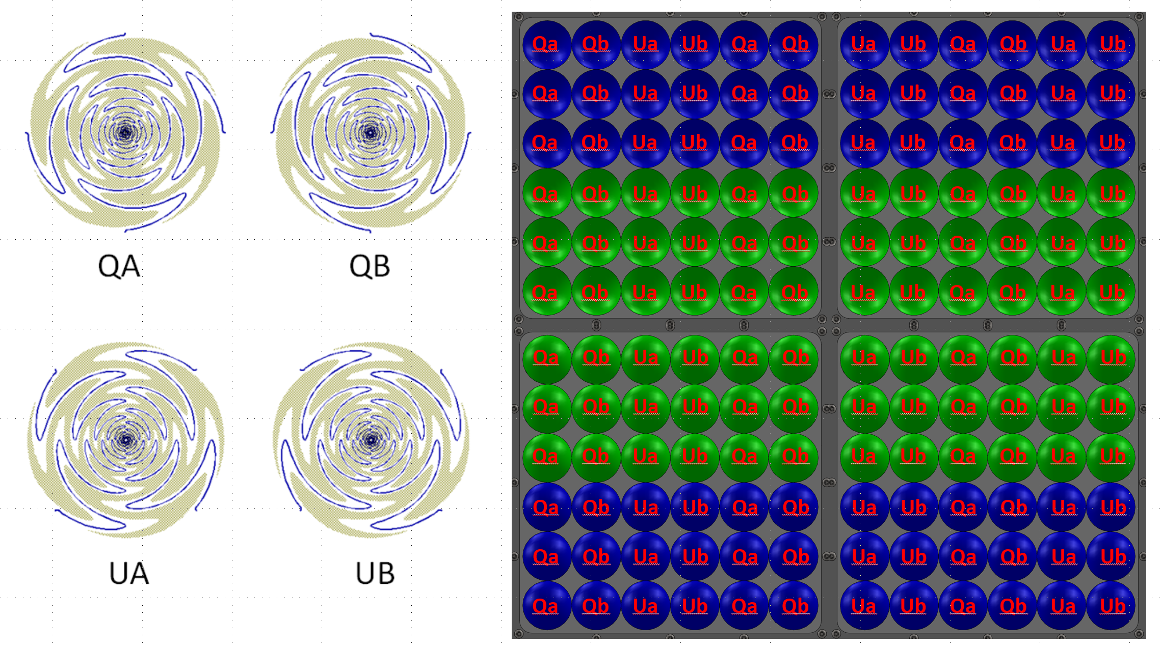
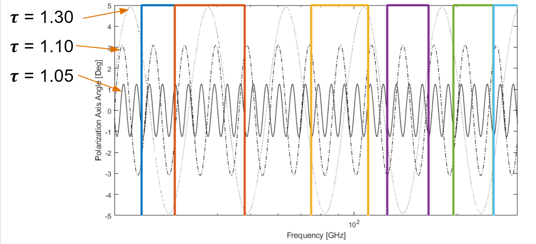
The log-periodic nature combined with inherent chirality of the sinuous antenna give rise to a small polarization rotation as function of frequency that can change within the bandwidth of a single Litebird band. The amplitude of this effect will be measured for all of the Litebird bands. Furthermore, we address this systematic effect by carefully choosing the orientation of the sinuous antennas that populate a FPM. We align the two axes of a sinuous antenna to the Q and U stokes parameters. We call the sinuous antennas with their micro-strips crossing at 0/90 degrees “Q” pixels and sinuous antennas with their micro-strips crossing at 45/135 degrees “U” pixels. For each of these pixel types we populate the focal plane with roughly half “A” type and “B” types, where type “B” is a mirror image of type “A” creating a natural cancellation of this rotation effect as shown in figure 5.
In addition to implementing this polarization rotation cancellation directly into the wafer design, the parameters that control the shape of the sinuous antenna can also be used to reduce the amplitude of the wobble, which makes this effect even more negligible.
3.2 Horn Coupled Orthomode Transducer Technology
Feedhorn coupled OMTs are widely used for studies of the polarization of the CMB as well as many other radio astronomy experiments [8, 12, 6]. In most modern experiments the feedhorns are either corrugated and/or have a spline profile which have nearly Gaussian beam profiles and have very small temperature to polarization (T to P) leakage over a large bandwidth [13]. The feedhorns also have excellent flexibility with respect to beam size and do not require any AR coatings, which can be especially challenging at the highest frequencies of Litebird.
The light coming through the feedhorn is coupled to four planar niobium OMT probes suspended on a low stress silicon nitride membrane. Each pair of Nb probes separate the orthogonal polarization components and couple them to separate CPW transmission lines. The CPWs are converted in to Nb micro-strip transmission lines and then split by stub filters into two distinct bands (see section 3.2.1). The power from each polarization and each band is sensed by a TES suspended on a bolometer island.
3.2.1 RF Components
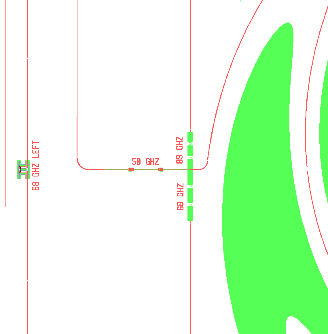
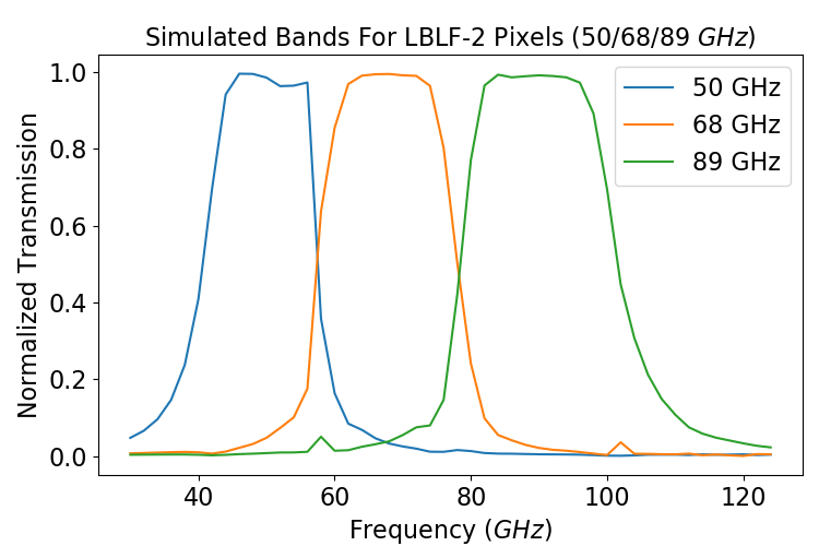
The details of the Radio-Frequency (RF) components vary from band to band and pixel to pixel, but the paradigm is the same for all of the pixels in Litebird as all of the arrays define the pass-bands directly on the wafer using a combination of CPW, low-loss superconducting micro-strip transmission lines, on wafer pass-band definition, cross-unders for orthogonal polarizations, and RF termination at the bolometer island. For Litebird the CPWs and micro-strip lines are constructed with Niobium and a low-loss SiNx layer. We pattern traditional RF circuit elements to the transmission lines to create the designed passbands. Table 2 summarizes the band centers and fractional bandwidths () for all of the Litebird bands, which is typically 30%. An example layout and simulated band passes for LF-2 are shown in figure 7. Simulation work is also complete for all of the other LF Litebird pixel types and fabrication and testing of these RF structures is underway. Initial results can be found in section 5.
3.3 TES Bolometers
The designs for the TES bolometers are quite similar for all 15 detector types due the fact that they share a common operating temperature and readout scheme. The thermal conductance is tuned to the expected optical load and then the heat capacity of each detector type is tuned so that all of the detectors have the same of 33 . The details of each band and expected optical power are shown in table 2 and a summary of all of the common optical and bolometric parameters are show in table 3. These are preliminary values, but we expect these to carry through with little or no change.
| Index | Band Center () | FPU | FPM | Pixel Size () | Optical Load () | () | ||
| 1 | 40 | LF | LF12 | 48 | 32 | 0.30 | 0.2918 | 114.63 |
| 2 | 50 | LF | LF12 | 24 | 32 | 0.30 | 0.306 | 72.48 |
| 3 | 60 | LF | LF12 | 48 | 32 | 0.23 | 0.2419 | 10.54 |
| LF | LF12 | 24 | 32 | 0.2709 | 15.70 | |||
| \rowcolorwhite 4 | 68 | LF | LF34 | 144 | 16 | 0.23 | 0.3279 | 9.84 |
| \rowcolorgray!25 | LF | LF12 | 48 | 32 | 0.2686 | 9.46 | ||
| 5 | 78 | LF | LF34 | 144 | 16 | 0.23 | 0.3272 | 7.69 |
| LF | LF12 | 24 | 32 | 0.2958 | 14.22 | |||
| \rowcolorwhite 6 | 89 | LF | LF34 | 144 | 16 | 0.23 | 0.3163 | 6.07 |
| \rowcolorgray!25 | LF | LF34 | 144 | 12 | 0.3061 | 5.11 | ||
| 7 | 100 | MF | MF1 | 366 | 12 | 0.23 | 0.3559 | 4.19 |
| LF | LF34 | 144 | 12 | 0.3765 | 3.82 | |||
| \rowcolorwhite 8 | 119 | MF | MF2 | 488 | 12 | 0.23 | 0.4386 | 2.82 |
| \rowcolorgray!25 | LF | LF34 | 144 | 12 | 0.3557 | 3.58 | ||
| 9 | 140 | MF | MF1 | 488 | 12 | 0.30 | 0.4206 | 3.16 |
| 10 | 166 | MF | MF2 | 488 | 12 | 0.30 | 0.3908 | 2.75 |
| MF | MF1 | 366 | 12 | 0.3572 | 3.48 | |||
| \rowcolorgray!25 11 | 195 | HF | HF1 | 254 | 6.6 | 0.30 | 0.6289 | 5.19 |
| \rowcolorwhite 12 | 235 | HF | HF2 | 254 | 6.6 | 0.30 | 0.4708 | 5.34 |
| \rowcolorgray!25 13 | 195 | HF | HF1 | 254 | 6.6 | 0.30 | 0.3770 | 0.682 |
| \rowcolorwhite 14 | 337 | HF | HF2 | 254 | 6.6 | 0.30 | 0.2997 | 10.85 |
| \rowcolorgray!25 15 | 402 | HF | HF3 | 338 | 5.7 | 0.23 | 0.2203 | 23.45 |
| Design | Goal |
| Pixel in-band optical efficiency | 80% |
| Minimum Operating Power | 2-3X optical power |
| On-sky end-to-end yield | 80% |
| FPU | 100 |
| Cross wafer variation | 7% |
| TES operating resistance | 0.6 to 0.8 |
| Parasitic series resistance | 0.05 to 0.2 |
| Intrinsic Time Constant () | 33 |
| Loopgain during operation | 10 |
| Common 1/f-knee | 20 |
| FPU lifetime | 3 years |
3.3.1 Interface to Cryogenic Readout
The same niobium layer that forms the micro-strip layer is also used to route the TES bias/readout leads to the edges of the wafer to interface with the readout. For the LF FPMs wiring density is low compared to ground-based arrays allowing for all of the TESs to be readout on a single side allowing for more flexibility with the design of the Cryogenic Readout (CR) interface. For the MF and HF FPMs the wires are routed to all of the edges of the wafer for bonding.
3.3.2 Cosmic Ray Mitigation
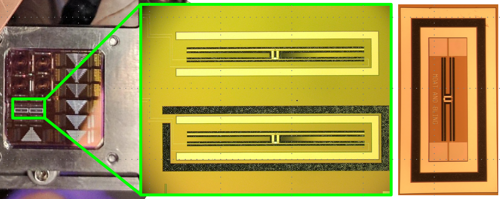
Cosmic ray mitigation is integrated directly into the focal plane design to limit cosmic ray impacts on low- systematics and data loss. The transient energy deposition of cosmic rays interacting with the spacecraft can create glitches in the time-stream of data sent to the readout. It is known from the Planck mission that long time scale glitches are produced when cosmic rays interact with the silicon die and short pulse-like glitches result from interactions close to the thermistor [14]. This has yielded a strategy of increasing thermal conductivity between the silicon die and the focal plane structures to reduce long time scale thermal fluctuations and blocking phonon propagation to the TES for the short glitches. To accomplish this we deposit a layer of Pd over the entire wafer where it does not interfere with the optical path nor with the Nb wiring. Progress in the lab has been made blocking the ballistic phonons near the TES by removing and adding metal layers and etching silicon. Examples of these mitigation structures are shown in figure 8.
In parallel to mitigation solutions, we are developing an end-to-end simulation tool to address the potential impact of cosmic rays on the data. The thermal impact of the particles is simulated in COMSOL assuming the cosmic ray environment at L2 as observed by PAMELA in 2009[15]. Thermal fluctuations of the wafer temperature, which is considered to be the bath temperature seen by the detectors, are then fed to a python routine111https://github.com/tomma90/tessimdc which simulates the detector response assuming a DC-biased configuration according to the model described in [16]. Although we expect different optical loading depending on the observing frequency, for simplicity we are assuming a typical optical loading of 0.5 pW. From this value we fix the saturation power to times the optical power, and by assuming a detector intrinsic time-constant of 33 ms we can define all parameters needed for the simulation. After computing the current response of the detector in the high loop gain limit () we convert the current to input power from the current responsivity in this limit . The generated detector timestream, for 12 TES on each wafer, is then fed to a satellite simulation pipeline developed for Litebird (TOAST-Litebird). The final results are , , and for each frequency band, for 12 TES, of only the cosmic ray effect. Using this end-to-end simulator, we plan to probe various design changes (e.g. the addition of Au wirebonds to the periphery of the wafer) in order to optimise Litebird’s mitigation of cosmic rays [17].
4 Fabrication
Litebird requires a total of 18 flight quality wafers to meet the sensitivity requirements. The responsibility of these wafers is split between the MNL at UC Berkeley and the BMF at NIST. UC Berkeley will fabricate the 8 LF wafers as well as the all of lenslet arrays for the LF-FPU and the MF-FPU. NIST will fabricate the MF and HF detector arrays and the feedhorn array for the HF-FPU.
4.1 Sinuous Antenna Fabrication
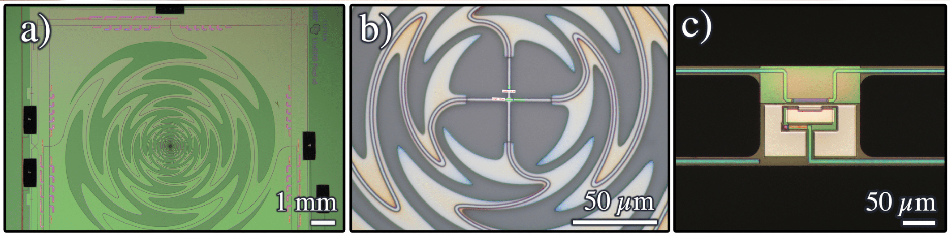
Although there are differences between the fabrication flow of sinuous antenna bolometers at MNL and BMF, we only describe the fabrication process for the sinuous antennas at UC Berkeley [7] to build a prototype LF-4 array. NIST has also completed the design and fabrication of a LF-1 prototype pixel as shown in Figure 9.
In the UC Berkeley fabrication proess flow starts with six inch p-doped 10-30 -square wafers that have had deposited a 600 structural film of low pressure chemical vapor deposition (LPCVD) low Stress nitride (LSN), with a buffer layer of 35 thermal oxide. From there, a Nb ground plane, is sputter deposited on the LSN surface with a film which is stress tuned to a compressive stress of -200. The tool dedicated to depositing the superconducting Nb, an MRC-943, is also used to deposit the TES AlMn (aluminum manganese) metal. The tool is used for these metals only, providing a high level of process control over the material properties and uniformity of these films. A base pressure in the low 10E-7T’s is maintained, with partial pressures of H2O, OH, and N2 into the 10E-8T’s. Cross wafer uniformity of sheet resistance for the Nb and AlMn is 2.5% and 1.8% respectively, with a wafer-to-wafer deviation of less than 1%.
All photolithography is performed using a GCA-8500 I-line stepper with the exception of Nb wiring from the bond pads to the TESs, for which a contact aligner is used. The Nb etching is performed with a LAM TCP metal etcher using a chlorine chemistry. By removing the typical BCl3 co-flow of gas, a high degree of selectivity can be achieved over both the structural LSN to Nb ground plane, and dielectric nitride to Nb microstrip. Once the wafers exit the TCP etcher, they are immediately quenched with de-ionized (DI) water to clean away any residual Cl2 from the etch that would otherwise react with the water in the atmosphere to create HCl which damages the grain boundaries Nb, leading to loss of optical efficiency.
The next step is to deposit the dielectric silicon nitride (SiNx) layer for the microstrip using a plasma enhanced chemical vapor deposition (PECVD) process using an Oxford Plasmalab System 100. While typical recipes for PECVD nitride use some ratio of SiH4 (Silane) and NH3 (ammonia) to deposit the SiNx film, an ammonia-less recipe was developed using a ratio of 1000:15 standard cubic centimeters per minutes (SCCMs) of N2:SiH4. By removing NH3 from the reaction, with the nitrogen coming from simple nitrogen gas, the hydrogen contaminant from precursor gas is greatly reduced, leading to less lossy dielectric [18].
Once the dielectric deposition is complete, construction of the TES bolometer island begins with the Ti (titanium) load resistor. A 40 film of Ti is deposited in a tool named MRC944, which is nearly identical to the MRC943 and benefits from the same high vacuum purity and repeatability process chamber with a cross wafer uniformity of 2%. The titanium load resistor is etched using the same LAM TCP metal etcher with a SF6/O2 chemistry. An in-situ, optical absorption end point detector is used to terminate the etch once the reactive gases etch through the Ti and reach the dielectric layer.
Next a 90 film of AlMn, using the MRC943, is deposited which is then lithographed and patterned into the TES. The etch is performed with a Phosphoric, Acetic, Nitirc (PAN) acid aluminum wet etch at 50∘C. The next step is to thermally tune the TESs for 10 minutes using a Wenesco vacuum hot plate which ensures a uniform thermal distribution across the wafer. A baking temperature of 188∘C was determined to produce a superconducting transition temperature of 160 in 90 AlMn films appropriate for Litebird TESs 12(d) [19].
Once the Ti load resistor and TES elements have been patterned, they are then protected by a 150 silicon nitride passivation layer. This is accomplished using a low temperature (25 ∘C) electron cyclotron resonance (ECR) based low pressure (10 ) PECVD which ensure that the of the TESs is not changed by this process. This passivation layer is patterned and etched using a LAM Oxide Rainbow etcher with CF4/O2 chemistry, such that the bulk of the Ti load resistors and TESs remain protected, with openings for electrical connection to the forthcoming Nb micro-strip and wiring layer.
The MRC943 is used again for the Nb sputter deposition, which forms the micro-strip and wiring. A sputter etch of the exposed Ti and AlMn ensures that native oxides are removed and a direct metal to metal contact is made. After the micro-strip, wiring and antenna are lithographically defined, the LAM metal etcher patterns the structures into the Nb.
The final layer to process is the thermal ballasts to tune the time constant of the bolometers to the readout bandwidth of the CR. We chose Pd (palladium) for its high thermal capacitance at low temperatures. This layer is patterned using a liftoff process which defines the structures with a 10 Ti adhesion layer and 1.0 m of Pd.
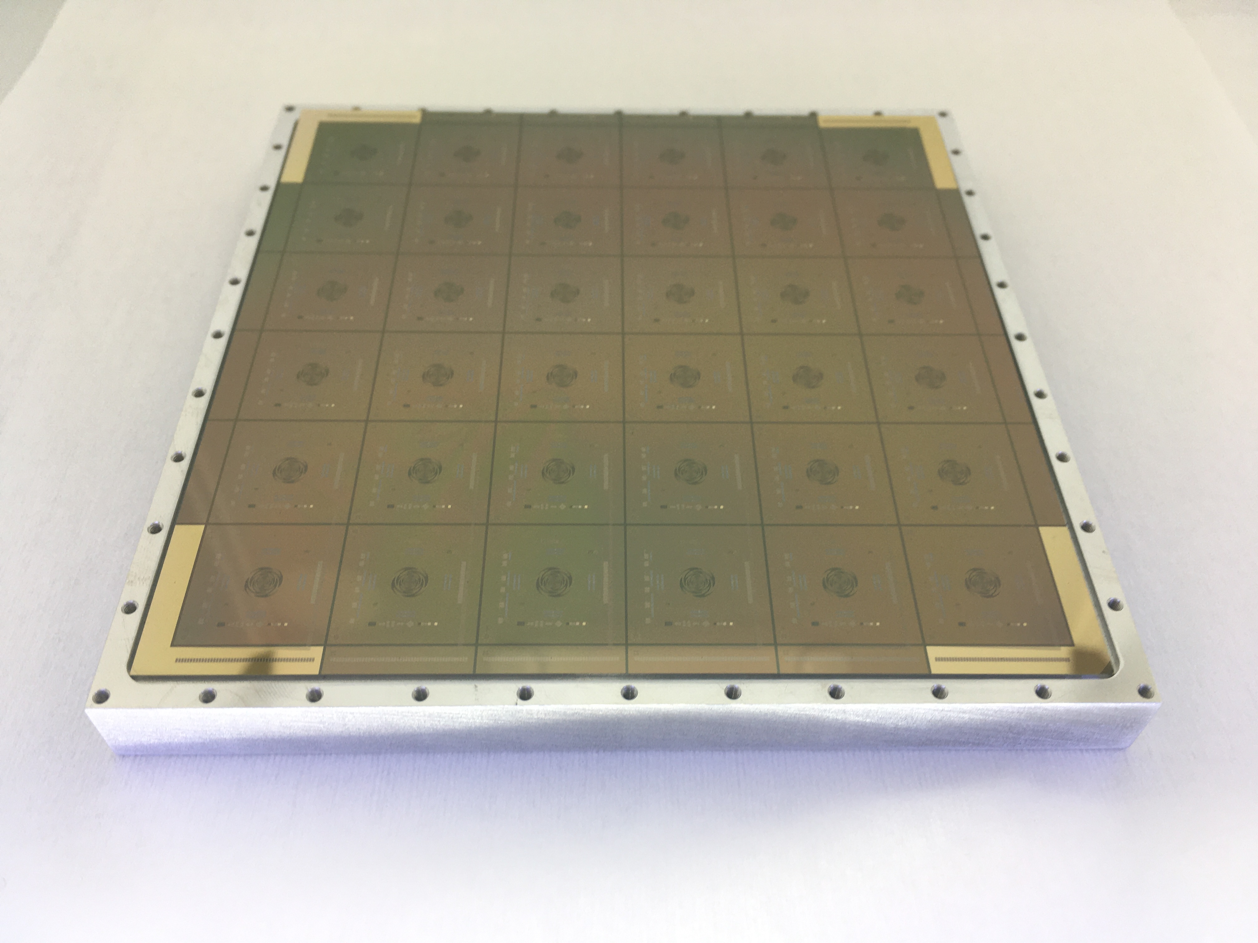
The final step is to thermally isolate the bolometer island from the bulk silicon substrate. This is accomplished by etching though the remaining LSN around the bolometer, to the silicon substrate. The wafer is diced into it’s final shape before being etched in an isotropic XeF2 vapor etch chamber that leaves the bolometer structure suspended and thermally isolated by etching the silicon substrate from underneath the bolometers. The buried thermal oxide layer, with its 1:1000 oxide to silicon selectivity, minimizes the amount of structural LSN consumed during the etch release from the silicon substrate. The final step is to ash away the photoresist that was protecting the metal detector elements from the XeF2 etch. A photograph of a completed array and bolometer is shown in figure 10.
4.2 OMT Fabrication
The OMT-coupled detector arrays are fabricated in the Class-100 NIST BMF cleanroom. The fabrication process for the OMT detector arrays borrows heavily from the processes developed at NIST for the high frequency 150/220 GHz Advanced ACTPol array [20, 8]. A 150 silicon (100) wafer is coated with 450 thermal SiOx and 1 m LPCVD low-stress SiNx, which together form the membranes that suspend the bolometer and OMT probes, as shown in figure 11(a). Additionally, the SiOx acts as the etch stop for the deep reactive ion etching (DRIE) step. All frontside patterning is completed with a dedicated 150 stepper, allowing for non-contact pattern transfer of every lithographic component.
The Nb ground plane and first wiring layer are sputter deposited, lithographically patterned, and plasma etched using a SF6/O2 ICP-RIE process. Next, the AlMn-alloy TES is sputter deposited, lithographically patterned, and wet etched with Transene Type A etchant heated to 50∘C. The patterned AlMn TES is annealed to 230∘C in air to set to the specified target of 160 . A SiNx dielectric layer, used for the microwave transmission lines, is deposited via PECVD, lithographically patterned, and etched in a CF4-based ICP-RIE plasma. The second Nb wiring layer, also used as the top microstrip conductor, is then sputter deposited, lithographically patterned, and plasma etched using a SF6-based ICP-RIE process. The RF termination is a meandering line of Ti/Au that is lithographically patterned for a liftoff process prior to an electron-beam evaporative deposition. A passivating SiNx dielectric layer is deposited with PECVD, then is lithographically patterned, and etched using a CF4-based ICP/RIE etch. PdAu thermal ballasts are added to the bolometer island by lithographically patterning for a liftoff process and sputter depositing the PdAu, which is chosen for its relatively high heat capacity. The bolometer leg geometry is defined by performing a frontside punch-through CF4-based ICP-RIE etch of all SiNx (PECVD-deposited and LPCVD-grown) and thermal SiOx.
The backside processing includes the blanket removal of both LPCVD SiNx and thermal oxide via SF6-based ICP-RIE etch. This allows for a backside liftoff process of electron-beam evaporated Ti/Au, which acts as a thermal heat sink in direct contact with the silicon wafer. Finally, the backside is lithographically patterned for the DRIE step, which both thermally isolates the bolometers from the silicon substrate via four SiNx legs and forms the SiNx/SiOx membrane on which the OMT probes are situated.
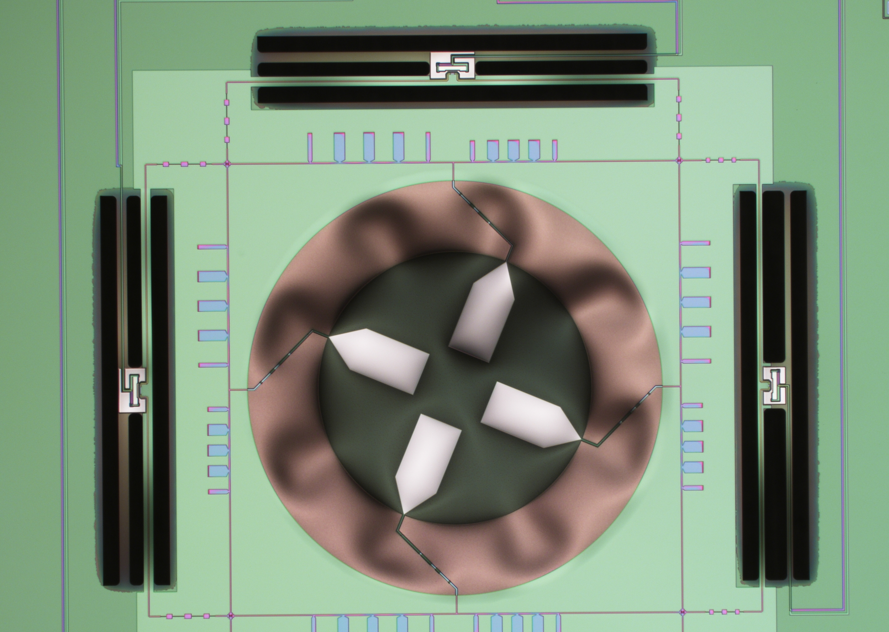
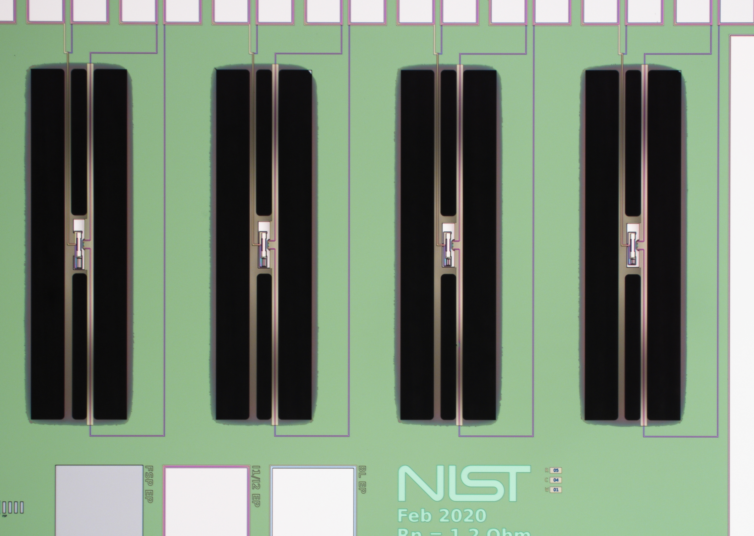
The NIST fabrication team has started on the production of prototype pixels for the HFT. Single pixel prototypes for the HF- are HF-2 bands have been fabricated and testing is ongoing. Figure 11(a) shows a micrograph of a completed Litebird HF-1 pixel and figure 11(b) shows a sampling of the accompanying prototype HF TES bolometers.
5 Testing
5.1 UC Berkeley
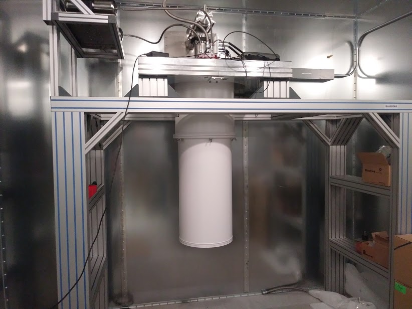
UC Berkeley has primary responsibility for the characterization of the LF-FPUs as well as the assembled LF-FPU. This will be carried in a BlueFors LD400 Dilution Refridgerator (DR) recently installed at UCB for the development of Litebird detectors. A photograph of this test-bed is shown in figure 12.
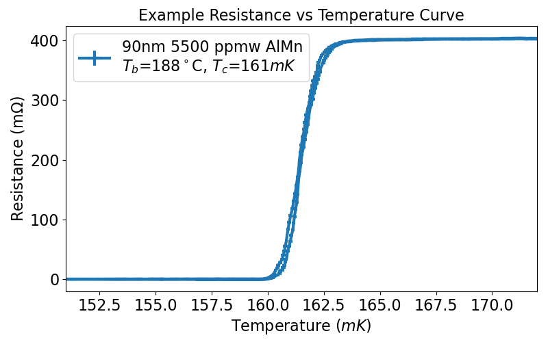
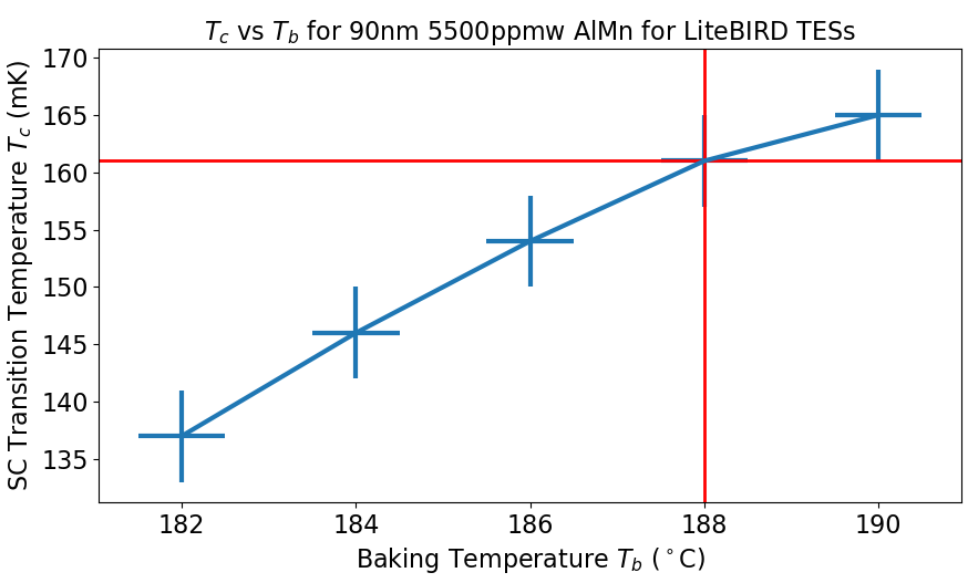
This 100 mK capable test bed is used for quick feed back of transition temperatures of the TES films as shown in figure 12(d). Based on heritage from building digital frequency-domain multiplexing (DfMux) appropriate TES sensor for the SA, the UC Berkeley fabrication team chose 90 films as the thickness for the Litebird TES of the LF-FPUs. A wafer with the same substrate as device wafer had 90 of AlMn deposited via DC magnetron sputtering. It was singulated into 1x1 cm squares, which were then thermally tuned at 5 different temperature ranging from 182 to 192∘C. A baking temperature of 188 ∘C yielded a of 160 which is the target specification for these TESs.
5.1.1 Cosmic Ray Mitigation
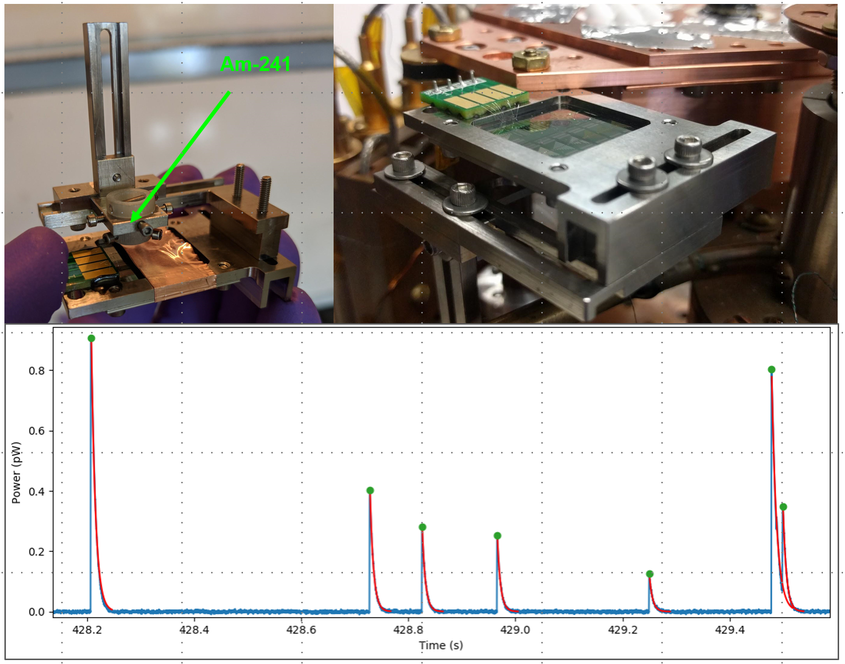
Tests with radioactive sources in the lab have shown phonon blocking effects by interrupting the phonon conduction paths to the TES [21]. 5.49 alpha particles from an Americium-241 source are used for measurements probing phonon propagation across the surface of the detector chips. To probe ballistic phonon propagation through the bulk silicon, a Cobalt-60 source, providing 1 gammas, is used. While the cobalt source can be placed outside of the dewar due to the highly penetrating gammas, the alpha particles from the Americium source will deposit almost all of their energy in the top layers of the device wafer. Because of this, the alpha source is mounted inside the cryostat with our detector chip in an invar assembly that allows for precise positioning of the source over the bolometers. The alpha source can be placed over a collimator which allows for illumination of specific components of the device wafer when desired. Bolometers underneath the source are arranged in a grid pattern to test both interaction distance as well as various mitigation. They are read out using a DC Superconducting Quantum Interference Device (SQUID), a pre-amplifier with a low pass filter and digital-to-analog converter (DAC) sampling at 6 . The resulting data is then fit using a matched filter peak finder and a second order polynomial in log-space as shown in figure 13.
5.2 CU Boulder
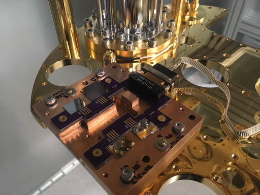
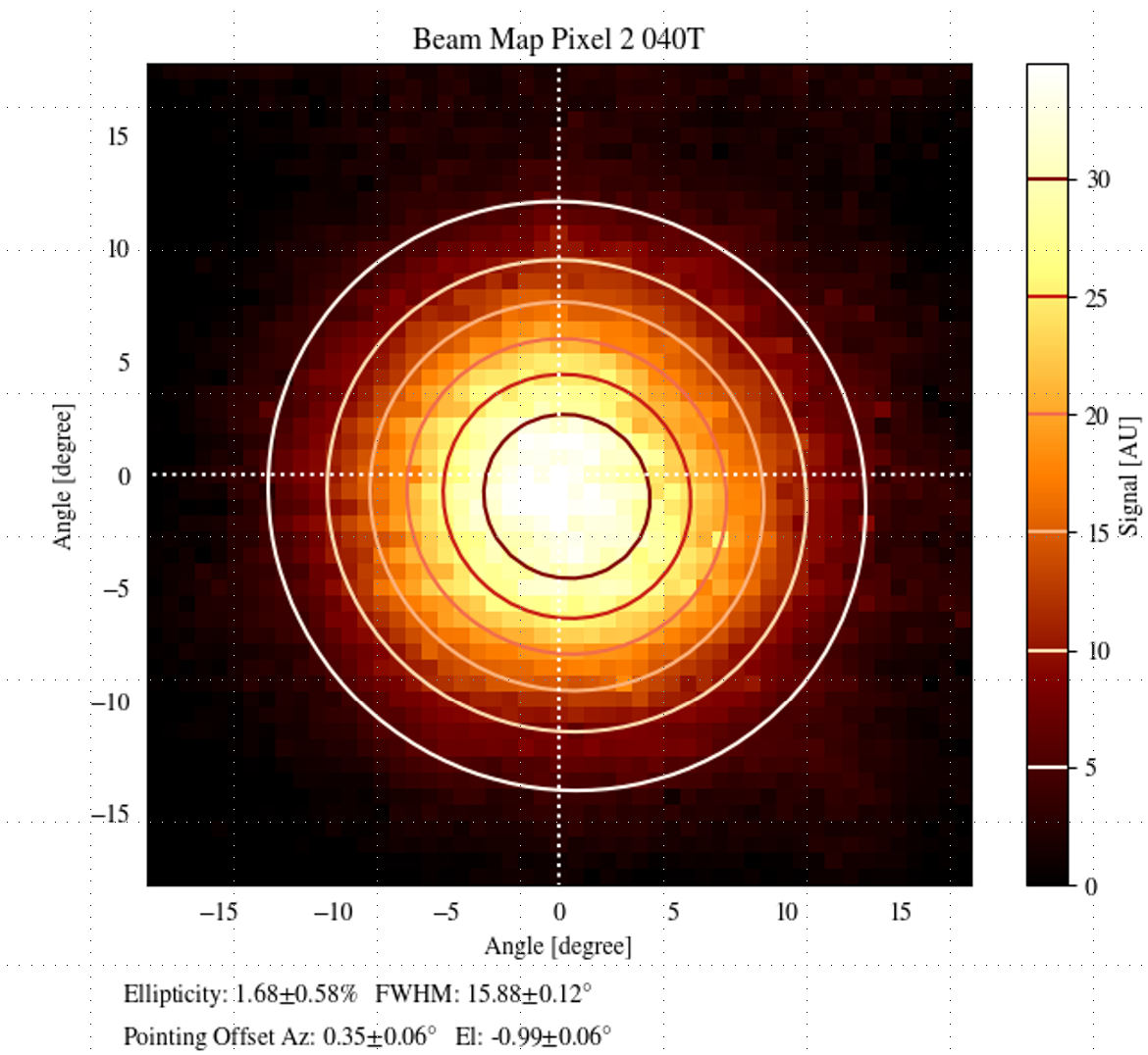
The CU is responsible for testing and characterization of the Mid-Frequency Focal Plane Modules (MF-FPMs). The CU test bed is a 100 2-stage ADR and has a heritage of testing detectors for South Pole Telescope Polarization Experiment (SPT-Pol), SPT-3G, POLARBEAR, and SA. The team has characterized Litebird prototype ”V0” LF-1 pixels and TES bolometers fabricated for Litebird research and development. characterized low-frequency pixels. The lab has a six-axis beam mapper and Fourier Transform Spectrometer (FTS) for detailed optical measurements of band and beam shape. Figure 14 shows details of the experimental setup and a beammap of 40 LF-1 bolometer.
Recently, the fabrication team at NIST finished HF-1 pixels which are slated to be tested at CU in the coming months.
5.3 Stanford
Stanford has primary responsibility for optical characterization of the high frequency FPMs. Sensitivity, polarization efficiency, feed pattern, spectral response, and temporal response will all be measured. The Stanford team also has primary responsibility for development of the FPU structures, and thus for testing the launch survival (at room temperature) of the units as well as microphonic transmission of representative units at cryogenic temperature. A shake table at Space Sciences Laboratory (Berkeley) will be used for launch survival testing, both of breadboard models and engineering models. Microphonics, as well as thermal loading and dimensional stability, will be measured and verified in-house.
6 Summary
In these proceedings, we report on the status of the US collaboration’s contribution to the Litebird satellite mission which will map the polarization CMB over the entire sky and constrain . The US will deliver three FM quality FPUs, for each of the mission’s three telescopes as a core contribution to the payload. The detector arrays will be fabricated at UC Berkeley and NIST and will be tested at Stanford, CU, and UC Berkeley with help from collaborators at other Litebird institutions.
Initial measurement of Litebird prototypes show that our designs to adapt ground based technology to a space environment is possible with further technical development. We built and characterized triplexing lenslet coupled sinuous antenna pixel appropriate for the LF-FPU with appropriate bandwidth in each band. In addition, we have characterized bolometers with correct and that meet the thermal-carrier noise requirements of the detection chain. We have designed and simulated many of the Litebird bands and have fabricated prototype pixels for the LF-FPU (LF-1 and LF-4) and HF-FPU (HF-1 and HF-2) pixel types and characterization is ongoing. Additionally, we are developing robust testing infrastructure and personnel training at all of the US Litebird institutions to meet the testing demands of delivering FM FPUs to the mission.
7 Acknowledgments
This work is supported in Japan by ISAS/JAXA for Pre-Phase A2 studies, by the acceleration program of JAXA research and development directorate, by the World Premier International Research Center Initiative (WPI) of MEXT, by the JSPS Core-to-Core Program of A. Advanced Research Networks, and by JSPS KAKENHI Grant Numbers JP15H05891, JP17H01115, and JP17H01125. The Italian LiteBIRD phase A contribution is supported by the Italian Space Agency (ASI Grants No. 2020-9-HH.0 and 2016-24-H.1-2018), the National Institute for Nuclear Physics (INFN) and the National Institute for Astrophysics (INAF). The French LiteBIRD phase A contribution is supported by the Centre National d’Etudes Spatiale (CNES), by the Centre National de la Recherche Scientifique (CNRS), and by the Commissariat à l’Energie Atomique (CEA). The Canadian contribution is supported by the Canadian Space Agency. The US contribution is supported by NASA grant no. 80NSSC18K0132. Norwegian participation in LiteBIRD is supported by the Research Council of Norway (Grant No. 263011). The Spanish LiteBIRD phase A contribution is supported by the Spanish Agencia Estatal de Investigación (AEI), project refs. PID2019-110610RB-C21 and AYA2017-84185-P. Funds that support contributions from Sweden come from the Swedish National Space Agency (SNSA/Rymdstyrelsen) and the Swedish Research Council (Reg. no. 2019-03959). The German participation in LiteBIRD is supported in part by the Excellence Cluster ORIGINS, which is funded by the Deutsche Forschungsgemeinschaft (DFG, German Research Foundation) under Germany’s Excellence Strategy (Grant No. EXC-2094 - 390783311). This research used resources of the Central Computing System owned and operated by the Computing Research Center at KEK, as well as resources of the National Energy Research Scientific Computing Center, a DOE Office of Science User Facility supported by the Office of Science of the U.S. Department of Energy.
References
- [1] M. Hazumi and L. J. S. Group, “Litebird satellite: Jaxa’s new strategic l-class mission for all-sky surveys of cosmic microwave background polarization,” Space Telescopes and Instrumentation 2020: Optical, Infrared, and Millimeter Wave, 2020 in preparation.
- [2] Y. Sekimoto and L. J. S. Group, “Wide field-of-view design of low frequency telescope on cmb b-mode polarization satellite litebird,” Space Telescopes and Instrumentation 2020: Optical, Infrared, and Millimeter Wave, 2020 in preparation.
- [3] L. Montier and L. J. S. Group, “Litebird mhft overview,” Space Telescopes and Instrumentation 2020: Optical, Infrared, and Millimeter Wave, 2020 in preparation.
- [4] K. Arnold, P. A. Ade, A. Anthony, F. Aubin, D. Boettger, J. Borrill, C. Cantalupo, M. Dobbs, J. Errard, D. Flanigan, et al., “The polarbear cmb polarization experiment,” in Millimeter, Submillimeter, and Far-Infrared Detectors and Instrumentation for Astronomy V, 7741, p. 77411E, International Society for Optics and Photonics, 2010.
- [5] F. W. Carter, T. W. Cecil, C. L. Chang, H.-M. Cho, J.-F. Cliche, T. M. Crawford, A. Cukierman, E. V. Denison, T. de Haan, J. Ding, M. A. Dobbs, D. Dutcher, W. Everett, A. Foster, J. C. Groh, A. Gilbert, N. W. Halverson, A. H. Harke-Hosemann, N. L. Harrington, J. W. Henning, G. C. Hilton, G. P. Holder, W. L. Holzapfel, N. Huang, K. D. Irwin, O. B. Jeong, M. Jonas, T. S. Khaire, L. Knox, A. M. Kofman, M. Korman, D. L. Kubik, S. Kuhlmann, C.-L. Kuo, A. T. Lee, E. M. Leitch, A. E. Lowitz, S. S. Meyer, D. Michalik, J. Montgomery, A. Nadolski, T. Natoli, H. Ngyuen, G. I. Noble, V. Novosad, S. Padin, Z. Pan, J. Pearson, C. M. Posada, A. Rahlin, C. L. Reichardt, J. E. Ruhl, J. T. Sayre, E. Shirokoff, G. Smecher, J. A. Sobrin, A. A. Stark, K. T. Story, A. Suzuki, K. L. Thompson, C. Tucker, L. R. Vale, K. Vanderlinde, J. Vieira, G. Wang, N. Whitehorn, V. Yefremenko, K. W. Yoon, M. Young, A. N. Bender, P. A. R. Ade, Z. Ahmed, A. J. Anderson, J. S. Avva, P. S. Barry, R. B. Thakur, B. A. Benson, L. S. Bleem, K. Byrum, J. E. Carlstrom, K. Aylor, S. Bocquet, S. Dodelson, J. Gallicchio, S. Guns, W. Quan, S. Raghunathan, W. L. Wu, and A. Jones, “Year two instrument status of the SPT-3g cosmic microwave background receiver,” in Millimeter, Submillimeter, and Far-Infrared Detectors and Instrumentation for Astronomy IX, J. Zmuidzinas and J.-R. Gao, eds., SPIE, Aug. 2018.
- [6] A. S. Bergman, P. A. R. Ade, S. Akers, M. Amiri, J. A. Austermann, J. A. Beall, D. T. Becker, S. J. Benton, J. J. Bock, J. R. Bond, S. A. Bryan, H. C. Chiang, C. R. Contaldi, R. S. Domagalski, O. Doré, S. M. Duff, A. J. Duivenvoorden, H. K. Eriksen, M. Farhang, J. P. Filippini, L. M. Fissel, A. A. Fraisse, K. Freese, M. Galloway, A. E. Gambrel, N. N. Gandilo, K. Ganga, A. Grigorian, R. Gualtieri, J. E. Gudmundsson, M. Halpern, J. Hartley, M. Hasselfield, G. Hilton, W. Holmes, V. V. Hristov, Z. Huang, J. Hubmayr, K. D. Irwin, W. C. Jones, A. Khan, C. L. Kuo, Z. D. Kermish, S. Li, P. V. Mason, K. Megerian, L. Moncelsi, T. A. Morford, J. M. Nagy, C. B. Netterfield, M. Nolta, B. Osherson, I. L. Padilla, B. Racine, A. S. Rahlin, S. Redmond, C. Reintsema, L. J. Romualdez, J. E. Ruhl, M. C. Runyan, T. M. Ruud, J. A. Shariff, E. C. Shaw, C. Shiu, J. D. Soler, X. Song, A. Trangsrud, C. Tucker, R. S. Tucker, A. D. Turner, J. Ullom, J. F. van der List, J. Van Lanen, M. R. Vissers, A. C. Weber, I. K. Wehus, S. Wen, D. V. Wiebe, and E. Y. Young, “280 GHz Focal Plane Unit Design and Characterization for the Spider-2 Suborbital Polarimeter,” Journal of Low Temperature Physics 193, pp. 1075–1084, Dec. 2018.
- [7] B. Westbrook, P. A. R. Ade, M. Aguilar, Y. Aklba, K. Arnold, C. Baccigalupi, D. Barron, D. Beck, S. Beckman, and A. N. Bender, “The polarbear-2 and simons array focal plane fabrication status,” Journal of Low Temperature Physics (5).
- [8] K. T. Crowley, J. E. Austermann, S. K. Choi, S. M. Duff, P. A. Gallardo, S.-P. P. Ho, J. Hubmayr, B. J. Koopman, F. Nati, M. D. Niemack, M. Salatino, S. M. Simon, S. T. Staggs, J. R. Stevens, J. N. Ullom, E. M. Vavagiakis, and E. J. Wollack, “Advanced ACTPol TES Device Parameters and Noise Performance in Fielded Arrays,” Journal of Low Temperature Physics 193, pp. 328–336, Nov. 2018.
- [9] A. Suzuki, P. Ade, Y. Akiba, C. Aleman, K. Arnold, C. Baccigalupi, B. Barch, D. Barron, A. Bender, D. Boettger, J. Borrill, S. Chapman, Y. Chinone, A. Cukierman, M. Dobbs, A. Ducout, R. Dunner, T. Elleflot, J. Errard, G. Fabbian, S. Feeney, C. Feng, T. Fujino, G. Fuller, A. Gilbert, N. Goeckner-Wald, J. Groh, T. D. Haan, G. Hall, N. Halverson, T. Hamada, M. Hasegawa, K. Hattori, M. Hazumi, C. Hill, W. Holzapfel, Y. Hori, L. Howe, Y. Inoue, F. Irie, G. Jaehnig, A. Jaffe, O. Jeong, N. Katayama, J. Kaufman, K. Kazemzadeh, B. Keating, Z. Kermish, R. Keskitalo, T. Kisner, A. Kusaka, M. L. Jeune, A. Lee, D. Leon, E. Linder, L. Lowry, F. Matsuda, T. Matsumura, N. Miller, K. Mizukami, J. Montgomery, M. Navaroli, H. Nishino, J. Peloton, D. Poletti, G. Puglisi, G. Rebeiz, C. Raum, C. Reichardt, P. Richards, C. Ross, K. Rotermund, Y. Segawa, B. Sherwin, I. Shirley, P. Siritanasak, N. Stebor, R. Stompor, J. Suzuki, O. Tajima, S. Takada, S. Takakura, S. Takatori, A. Tikhomirov, T. Tomaru, B. Westbrook, N. Whitehorn, T. Yamashita, A. Zahn, and O. Zahn, “The Polarbear-2 and the Simons Array Experiments,” Journal of Low Temperature Physics 184, pp. 805–810, Aug. 2016.
- [10] F. W. Carter, T. W. Cecil, C. L. Chang, H.-M. Cho, J.-F. Cliche, T. M. Crawford, A. Cukierman, E. V. Denison, T. de Haan, J. Ding, M. A. Dobbs, D. Dutcher, W. Everett, A. Foster, J. C. Groh, A. Gilbert, N. W. Halverson, A. H. Harke-Hosemann, N. L. Harrington, J. W. Henning, G. C. Hilton, G. P. Holder, W. L. Holzapfel, N. Huang, K. D. Irwin, O. B. Jeong, M. Jonas, T. S. Khaire, L. Knox, A. M. Kofman, M. Korman, D. L. Kubik, S. Kuhlmann, C.-L. Kuo, A. T. Lee, E. M. Leitch, A. E. Lowitz, S. S. Meyer, D. Michalik, J. Montgomery, A. Nadolski, T. Natoli, H. Ngyuen, G. I. Noble, V. Novosad, S. Padin, Z. Pan, J. Pearson, C. M. Posada, A. Rahlin, C. L. Reichardt, J. E. Ruhl, J. T. Sayre, E. Shirokoff, G. Smecher, J. A. Sobrin, A. A. Stark, K. T. Story, A. Suzuki, K. L. Thompson, C. Tucker, L. R. Vale, K. Vanderlinde, J. Vieira, G. Wang, N. Whitehorn, V. Yefremenko, K. W. Yoon, M. Young, A. N. Bender, P. A. R. Ade, Z. Ahmed, A. J. Anderson, J. S. Avva, P. S. Barry, R. B. Thakur, B. A. Benson, L. S. Bleem, K. Byrum, J. E. Carlstrom, K. Aylor, S. Bocquet, S. Dodelson, J. Gallicchio, S. Guns, W. Quan, S. Raghunathan, W. L. Wu, and A. Jones, “Year two instrument status of the SPT-3g cosmic microwave background receiver,” in Millimeter, Submillimeter, and Far-Infrared Detectors and Instrumentation for Astronomy IX, J. Zmuidzinas and J.-R. Gao, eds., SPIE, Aug. 2018.
- [11] N. Galitzki, A. Ali, K. S. Arnold, P. C. Ashton, J. E. Austermann, C. Baccigalupi, T. Baildon, D. Barron, J. A. Beall, S. Beckman, S. M. M. Bruno, S. Bryan, P. G. Calisse, G. E. Chesmore, Y. Chinone, S. K. Choi, G. Coppi, K. D. Crowley, K. T. Crowley, A. Cukierman, M. J. Devlin, S. Dicker, B. Dober, S. M. Duff, J. Dunkley, G. Fabbian, P. A. Gallardo, M. Gerbino, N. Goeckner-Wald, J. E. Golec, J. E. Gudmundsson, E. E. Healy, S. Henderson, C. A. Hill, G. C. Hilton, S.-P. P. Ho, L. A. Howe, J. Hubmayr, O. Jeong, B. Keating, B. J. Koopman, K. Kiuchi, A. Kusaka, J. Lashner, A. T. Lee, Y. Li, M. Limon, M. Lungu, F. Matsuda, P. D. Mauskopf, A. J. May, N. McCallum, J. McMahon, F. Nati, M. D. Niemack, J. L. Orlowski-Scherer, S. C. Parshley, L. Piccirillo, M. S. Rao, C. Raum, M. Salatino, J. S. Seibert, C. Sierra, M. Silva-Feaver, S. M. Simon, S. T. Staggs, J. R. Stevens, A. Suzuki, G. Teply, R. Thornton, C. Tsai, J. N. Ullom, E. M. Vavagiakis, M. R. Vissers, B. Westbrook, E. J. Wollack, Z. Xu, and N. Zhu, “The Simons Observatory: instrument overview,” in Millimeter, Submillimeter, and Far-Infrared Detectors and Instrumentation for Astronomy IX, J. Zmuidzinas and J.-R. Gao, eds., 10708, pp. 1 – 13, International Society for Optics and Photonics, SPIE, 2018.
- [12] J. E. Austermann, K. A. Aird, J. A. Beall, D. Becker, A. Bender, B. A. Benson, L. E. Bleem, J. Britton, J. E. Carlstrom, C. L. Chang, H. C. Chiang, H.-M. Cho, T. M. Crawford, A. T. Crites, A. Datesman, T. de Haan, M. A. Dobbs, E. M. George, N. W. Halverson, N. Harrington, J. W. Henning, G. C. Hilton, G. P. Holder, W. L. Holzapfel, S. Hoover, N. Huang, J. Hubmayr, K. D. Irwin, R. Keisler, J. Kennedy, L. Knox, A. T. Lee, E. Leitch, D. Li, M. Lueker, D. P. Marrone, J. J. McMahon, J. Mehl, S. S. Meyer, T. E. Montroy, T. Natoli, J. P. Nibarger, M. D. Niemack, V. Novosad, S. Padin, C. Pryke, C. L. Reichardt, J. E. Ruhl, B. R. Saliwanchik, J. T. Sayre, K. K. Schaffer, E. Shirokoff, A. A. Stark, K. Story, K. Vanderlinde, J. D. Vieira, G. Wang, R. Williamson, V. Yefremenko, K. W. Yoon, and O. Zahn, “SPTpol: an instrument for CMB polarization measurements with the South Pole Telescope,” in Millimeter, Submillimeter, and Far-Infrared Detectors and Instrumentation for Astronomy VI, W. S. Holland, ed., 8452, pp. 393 – 410, International Society for Optics and Photonics, SPIE, 2012.
- [13] M. H. Abitbol, Z. Ahmed, D. Barron, R. B. Thakur, A. N. Bender, B. A. Benson, C. A. Bischoff, S. A. Bryan, J. E. Carlstrom, C. L. Chang, D. T. Chuss, K. T. Crowley, A. Cukierman, T. de Haan, M. Dobbs, T. Essinger-Hileman, J. P. Filippini, K. Ganga, J. E. Gudmundsson, N. W. Halverson, S. Hanany, S. W. Henderson, C. A. Hill, S.-P. P. Ho, J. Hubmayr, K. Irwin, O. Jeong, B. R. Johnson, S. A. Kernasovskiy, J. M. Kovac, A. Kusaka, A. T. Lee, S. Maria, P. Mauskopf, J. J. McMahon, L. Moncelsi, A. W. Nadolski, J. M. Nagy, M. D. Niemack, R. C. O’Brient, S. Padin, S. C. Parshley, C. Pryke, N. A. Roe, K. Rostem, J. Ruhl, S. M. Simon, S. T. Staggs, A. Suzuki, E. R. Switzer, O. Tajima, K. L. Thompson, P. Timbie, G. S. Tucker, J. D. Vieira, A. G. Vieregg, B. Westbrook, E. J. Wollack, K. W. Yoon, K. S. Young, and E. Y. Young, “Cmb-s4 technology book, first edition,” 2017.
- [14] A. Catalano, P. Ade, Y. Atik, A. Benoit, E. Bréele, J. Bock, P. Camus, M. Charra, B. Crill, N. Coron, et al., “Characterization and physical explanation of energetic particles on planck hfi instrument,” Journal of Low Temperature Physics 176(5-6), pp. 773–786, 2014.
- [15] P. Picozza, A. Galper, G. Castellini, O. Adriani, F. Altamura, M. Ambriola, G. Barbarino, A. Basili, G. Bazilevskaja, R. Bencardino, et al., “Pamela–a payload for antimatter matter exploration and light-nuclei astrophysics,” Astroparticle physics 27(4), pp. 296–315, 2007.
- [16] K. Irwin and G. Hilton, Transition-Edge Sensors, pp. 63–150. Springer Berlin Heidelberg, Berlin, Heidelberg, 2005.
- [17] S. L. Stever, T. Ghigna, M. Tominaga, M. Tsujimoto, Y. Minami, S. Sugiyama, A. Kato, T. Matsumura, H. Ishino, and M. Hazumi, “Simulations of systematic effects arising from cosmic rays in the litebird space telescope, and effects on the measurements of cmb modes,” Journal of Cosmology and Astrophysics, 2020 in preparation.
- [18] T. e. a. Dominguez, “Material and optical properties of low-temperature NH3-free PECVD SiNx layers for photonic applications,”
- [19] D. Li, J. Austermann, J. Beall, D. Becker, S. Duff, P. Gallardo, S. Henderson, G. Hilton, S.-P. Ho, J. Hubmayr, B. Koopman, J. McMahon, F. Nati, M. Niemack, C. Pappas, M. Salatino, B. Schmitt, S. Simon, S. Staggs, and E. Wollack, “Almn transition edge sensors for advanced actpol,” Journal of Low Temperature Physics 184, 07 2016.
- [20] S. Duff, J. Austermann, J. Beall, D. Becker, R. Datta, P. Gallardo, S. Henderson, G. Hilton, S. Ho, J. Hubmayr, B. Koopman, D. Li, J. McMahon, F. Nati, M. Niemack, C. Pappas, M. Salatino, B. Schmitt, S. Simon, and E. Wollack, “Advanced actpol multichroic polarimeter array fabrication process for 150 mm wafers,” Journal of Low Temperature Physics 184, 08 2016.
- [21] S. M. Beckman, A. T. Lee, M. Hazumi, A. Suzuki, Y. Minami, N. A. Kurinsky, and L. Collaboration, “Development of cosmic ray mitigation techniques for the LiteBIRD space mission (Conference Presentation),” in Millimeter, Submillimeter, and Far-Infrared Detectors and Instrumentation for Astronomy IX, J. Zmuidzinas and J.-R. Gao, eds., 10708, International Society for Optics and Photonics, SPIE, 2018.