Multiple crossing of Landau levels of two-dimensional fermions in double HgTe quantum wells
Abstract
The double quantum well systems consisting of two HgTe layers separated by a tunnel-transparent barrier are expected to manifest a variety of phase states including two-dimensional gapless semimetal and two-dimensional topological insulator. The presence of several subbands in such systems leads to a rich filling factor diagram in the quantum Hall regime. We have performed magnetotransport measurements of the HgTe-based double quantum wells in both gapless and gapped state and observed numerous crossings between the Landau levels belonging to different subbands. We analyze the Landau level crossing patterns and compare them to the results of theoretical calculations.
I Introduction
The energy band structure of two-dimensional (2D) carriers in HgTe quantum wells (QWs) konig is described by the Bernevig-Hughes-Zhang (BHZ) effective Hamiltonian bernevig , which is similar to the Dirac Hamiltonian for 2D fermions. This description accounts for intriguing properties observed experimentally, such as the existence of two-dimensional topological insulators (TI) with edge states konig ; hasan ; qi ; kane ; moore ; moore2 ; zhou ; roth ; gusev , massless Dirac fermions with band dispersion similar to that of graphene buttner ; kozlov ; gusev2 , and phase transitions between the ordinary insulator and the 2D TI. The double quantum wells (DQWs) consisting of two tunnel-coupled HgTe QWs, Fig. 1 (a), represent the simplest example of multilayer Dirac fermion system with variable properties. Such DQWs have been recently recognized as promising systems to explore the phase transition between topological and ordinary insulator states michetti ; kristopenko . The additional degrees of freedom associated with tunnel-induced hybridization of different 2D subbands lead to a variety of possible phase states. The conditions for subband inversion corresponding to transitions between these states depend on the well width and on the coupling parameters, such as the thickness and height of the potential barrier separating the QWs kristopenko . The studies of HgTe-based DQWs are of particular interest in connection with possible realization of TIs with tunable gaps.
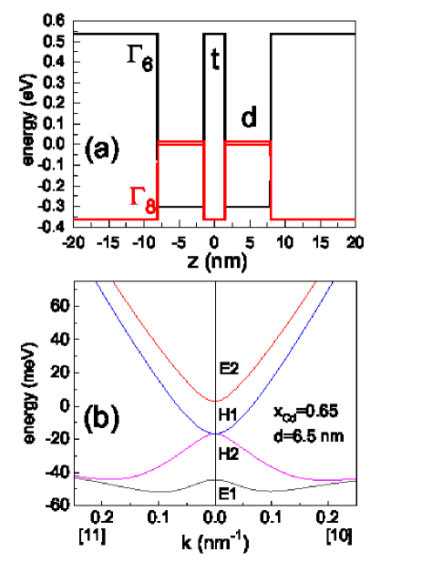
The diversity of phase states in HgTe DQWs is related to a negligible tunnel hybridization of the heavy hole subbands H1 and H2 at zero wave vector , so these subbands remain degenerate, while the electronlike subbands E1 and E2 experience a strong hybridization leading to a large energy separation between them. As a result, different kinds of subband ordering can occur. The fully inverted subband ordering E1-E2-H2-H1 naturally corresponds to the TI phase. On the other hand, the ”mixed” subband ordering E1-H2-H1-E2, which can be realized in a wide region of parameters, leads to the gapless spectrum in symmetric DQWs, as shown in Fig. 1 (b). This gapless spectrum resembles that of bilayer graphene castro , but with a crucial difference, the absence of the valley degeneracy. However, if the symmetry is broken by a transverse bias or electric field perpendicular to the 2D plane, the heavy hole subbands H1 and H2 become split apart. Thus, similar to the case of bilayer graphene castro ; mocann , a transverse electric field transforms the gapless phase into a gapped (insulating) phase kristopenko . In contrast to bilayer graphene, where the gapped state is an ordinary insulator, the gapped state in HgTe DQWs is expected to be a 2D TI. Indeed, the inverted subband ordering, when E1 falls below H1 and H2, leads to coexistence of the bulk and edge states, and when the gap opens in the bulk, the edge states remain gapless in view of the time reversal symmetry. Recent studies gusevnew confirm the existence of the gap and edge state transport both in symmetric and asymmetric DQWs, as well as the existence of the gapless phase, in accordance with theoretical predictions.
Application of a magnetic field perpendicular to the layers leads to Landau quantization and allows one to get additional information about electronic properties of the systems with Dirac-like band spectrum. In single layer systems, it makes possible to distinguish between the gapless phase with Dirac cone dispersion (graphene and HgTe QWs) and gapped (TI and ordinary insulator) phases in HgTe QWs. In this case, there exists a single crossing of special Landau levels (LLs) with zero indices () belonging to conduction and valence subbands, which takes place in the TI phase konig ; castro ; peres ; sarma ; buttner . In contrast to single layer systems, the LL spectrum both in bilayer graphene and in HgTe-based DQWs is expected to show numerous LL crossings falko ; nilsson ; kristopenko ; koshino ; fogler . It is found that multiple LL crossing provides a useful tool for precise determination of the band structure parameters in trilayer graphene herrero ; stepanov ; datta . In bilayer graphene, observation of such crossing is unlikely because of large separation of subbands in energy space chung . On the other hand, in HgTe-based DQWs the subband energy separation is small (Fig. 1), which makes them unique, among the other systems with Dirac-like energy spectrum, for experimental studies of multiple LL crossing. Unlike the case of graphite multilayers, the absence of valley degeneracy in the HgTe structures allows for a completely reliable comparison between the theoretical LL spectrum and the experimentally observed LL crossing and splitting. Studies of the properties of energy spectrum of multilayer Dirac systems in magnetic field are important also in connection with a growing interest to the quantum Hall ferromagnetism datta and multicomponent fractional quantum Hall effect (QHE) papic .
Though experimental studies of HgTe DQWs in magnetic field are limited yakunin ; bovkun , they already demonstrate some features related to complex LL spectrum in these structures. In particular, studies of the QHE in the samples with hole type of conductivity reveal a reentrant quantization of Hall resistance yakunin . Magnetooptical spectra show shifts and doubling of the main magnetoabsorption lines bovkun . These features are in qualitative agreement with LL spectrum calculation based on the Kane Hamiltonian. However, the magnetotransport measurements yakunin have been carried out in a narrow interval of carrier density, changed by illumination. While showing important aspects of the Landau quantization in the valence band, the results of Ref. yakunin do not give a comprehensive picture of LL spectrum. In particular, the behavior of LLs in the conduction band, where a regular pattern of multiple LL crossing is expected, and in the important region near the charge neutrality remains unexplored.
In this paper, we use DQW samples with a top gate which allows us to control the density of carriers in a wide interval and to determine the LL picture from magnetotransport measurements. We study two kinds of HgTe-based double quantum wells with different values of and . The DQW with nm, whose band diagram and energy spectrum are shown in Fig. 1, demonstrates the properties of gapless semimetal, while the DQW with nm shows an activation temperature dependence of conductivity corresponding to a small energy gap meV gusevnew . As the symmetric DQW with nm should also be in a gapless phase according to our calculations, the presence of the gap can be explained by an asymmetry, for example, the appearance of an internal electric field due to uncontrollable doping during the growth. For both DQWs, we have investigated the LL diagram and revealed multiple successive crossings between LLs in magnetic fields up to 8 T, resembling those observed in trilayer graphene herrero ; stepanov ; datta . For DQW with nm, we have studied behavior of the resistance near the charge neutrality point, which identifies the important crossing point for the LLs with and suggests that the degeneracy of H1 and H2 subbands is lifted as a result of application of the gate voltage. The observed properties of the energy spectrum are reproduced in our numerical calculations.
The paper is organized as follows. In Sec. II we provide the details of the sample fabrication and measurements, and describe the details of the calculations. In Sec. III we present the results of measurements of both the longitudinal and the Hall resistances in magnetic fields, compare them with similar measurements in single quantum wells, and discuss these results in correlation with the calculated LL spectra. The last section contains a brief summary and conclusions.
II Methods
The structures containing HgTe quantum well layers of equal widths separated by CdxHg1-xTe barriers, with surface orientation [013], were grown by molecular beam epitaxy (MBE). To prepare the gate, a dielectric layer (100 nm of SiO2 and 100 nm of Si3 Ni4) was first grown on the structure using the plasmochemical method, and then the TiAu gate was deposited. By studying two groups of samples with different parameters and , we have observed both the gapped TI and the gapless semimetal phases, distinguished by the temperature dependence of the local resistance. Table I contains the list of experimental samples and indicates the typical parameters, such as the well width , barrier thickness , barrier composition and gate voltage corresponding to the charge neutrality point (CNP) . By measuring nonlocal resistance in zero magnetic field in the gapped DQW samples with nm, we confirm the presence of the edge state transport in the absence of magnetic field gusev4 , thereby providing the experimental evidence of the 2D TI phase in HgTe DQWs gusevnew . Neither the activation behavior of the conductance nor the edge state transport are observed in the DQWs with nm, expected to be in the gapless phase gusevnew .
| (nm) | (nm) | Cd content | (V) | properties |
|---|---|---|---|---|
| 6.5 | 3 | 0.65 | -4.2 | gapless |
| 6.0 | 3 | 0.37 | -0.7 | gapped TI |
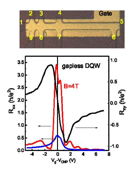
The quantum well width and the thickness of the barrier nm have been determined by using ellipsometry during the MBE growth. The samples are Hall bar devices with 2 current probes and 7 voltage probes. The bar has a width m and three consecutive segments of different lengths , 8, and 32 m (Fig. 2). Fabrication of ohmic contacts to HgTe quantum well is similar to that for other 2D systems, such as GaAs quantum wells: the contacts were formed by the burning of indium directly to the surface of large contact pads. The modulation-doped HgTe/CdHgTe quantum wells are typically grown at 180o C. Therefore, in contrast to III-V compounds, the temperatures during the contact fabrication process are relatively low. On each contact pad, the indium diffuses vertically down, providing an ohmic contact to both quantum wells, with the contact resistance in the range of 10-50 kOhm. During the AC measurements we always check that the Y-component of the impedance never exceed 5% of the total impedance, which demonstrates good ohmicity of the contacts. Three devices for each set of parameters were studied. The density variation with the gate voltage was cm-2V-1. The magnetotransport measurements were performed in the temperature range K by using a standard four-point circuit with a Hz ac current of nA through the sample, which is sufficiently low to avoid overheating effects. It is worth noting that in the presence of strong magnetic fields there may occur a resistance build-up in the mesa across the gate electrode edge due to carrier reflection. This is why we report the results only up to 4 T or 8 T, depending on the device. The current flows through the contacts 1 and 5, the longitudinal voltage is measured between the closest pair of voltage probes (9 and 8), and the Hall voltage is measured between the probes on the opposite sides of the Hall bar.
The numerical calculations of electron energy spectrum were based on the Kane Hamiltonian whose description with applications for different orientations of the heterointerface is given in Ref. raichev . The energy is counted from the band edge in HgTe, the relative band edge positions of the in HgTe, in CdTe, and in CdTe are eV, eV, and eV, respectively. The Kane matrix element and the Luttinger parameters , , and for HgTe and CdTe are taken from Ref. novik . Also, a strain-induced shift meV of light hole band with respect to heavy hole band in HgTe layer on CdTe substrate brune has been taken into account. Applying these parameters for the structures with CdxHg1-xTe barriers, we use a linear interpolation with respect to Cd content in order to find the band edge energies, Luttinger parameters in the barriers, and in HgTe layers. The energy spectra at zero , shown in Fig. 1, were calculated for [013] orientation of the interface. The LL spectra shown in Fig. 5 (a) and Fig. 6 (a) were calculated in the isotropic approximation, when was set equal to both in the wells and in the barrier layers (in this case the spectra do not depend on the orientation). The isotropic approximation strongly simplifies the numerical solution of eigenstate problem raichev1 and is expected to give reliable results for the conduction band spectrum, which is in the focus of attention in this paper.
III Results
In both kinds of DQW samples we study, the dependence of the resistance on the gate voltage in zero magnetic field (Fig. 2) shows a maximum near the CNP, resembling the one observed in the HgTe-based single quantum wells, including TIs konig ; roth ; gusev2 and 6.3 nm-wide QWs with massless Dirac fermions buttner ; kozlov ; gusev . In order to probe the nature of the transport in the DQWs, we have measured the temperature dependence of the conductance near the CNP. The results are briefly described below. A detailed description can be found in Ref. gusevnew . While in narrow-gap samples one would expect a thermally activated conductance (see, for example, a review paper gusev4 ), the DQW with nm shows a quasi-metallic behavior, the resistance is saturated for K and increases with at higher temperatures. A similar temperature dependence has been observed for the gapless Dirac fermion system in a single 6.3 nm HgTe well buttner ; kozlov ; gusev . The other DQW with lower Cd content, , nm, and nm, shows an insulating temperature dependence described by the activation law at K. The thermally activated behavior corresponds to a gap of energy meV between the conduction and the valence bands. This finding can be explained by the presence of an asymmetry, presumably related to the specifics of the MBE growth for this particular structure, such as an uncontrollable chemical doping. Our calculations demonstrate that the observed gap can be created by a transverse electric field kV/cm. The results of earlier experiments on HgTe DQWs yakunin ; bovkun also suggest the presence of transverse electric field. While in bilayer graphene the transverse electric field can be controlled by double gates maher , the MBE-grown HgTe DQWs with controllable gap are still not available technologically.
The measurements of longitudinal and the Hall resistances in a perpendicular magnetic field demonstrates the QHE behavior: the resistance minima are accompanied with the Hall resistance plateaux (Fig. 2). We first compare the magnetotransport in the gapless DQW with that in the gapless single QW. Figures 3 and 4 shows the longitudinal and Hall conductivities as functions of both the gate voltage and the magnetic field for these two structures. At the CNP, the longitudinal conductivity drops to zero, while the Hall one changes its sign in both kinds of structures. The quantum Hall state with zero filling factor differs from the states with . Indeed, for the states with both the longitudinal conductivity and the longitudinal resistivity turn to zero, while for the QHE state the longitudinal resistance shows a maximum rather than a minimum, , and we obtain abanin . Early experiments on the quantum Hall effect in bilayer graphene have confirmed an important theoretical prediction falko that the nearest to the CNP Hall conductivity plateau has the value , which is two times larger than that in a single layer graphene due to the additional degeneracy of the zeroth Landau level. However, in high-mobility samples in a strong magnetic field a complete symmetry breaking takes place and the QHE states appear at all integer filling factors velasco ; maher ; weitz ; lee . In our HgTe DQW samples, the Hall conductivity plateaux are also observed at all integer filling factors, because the valley degeneracy is absent and the Zeeman splitting is large enough. While in a single QW shows regular peaks and minima, in DQWs is less regular and shows modulations of Shubnikov-de Haas oscillations because of superposition of the contributions from LLs belonging to different 2D subbands.
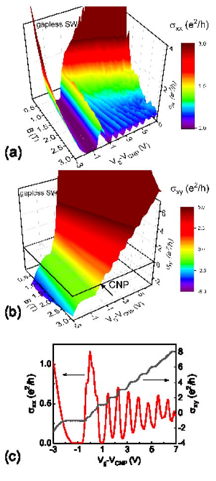
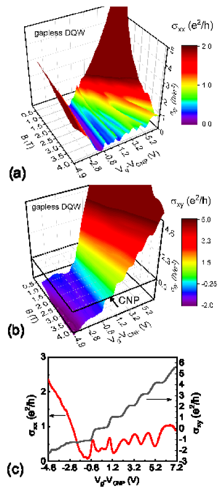
Now we turn to a detailed comparison between the experimental resistance plot of and the theoretical LL spectrum. The fan chart in Fig. 5 (a) shows the LL energies as functions of for the gapless DQW. Here is the LL index and is the subband index. Some of the LLs are marked by the index . The conduction band part consists of two sets of levels originating from the E2 and H1 subbands, see Fig. 1 (b). The nonlinear dependence of LL energies on is characteristic for relativistic Dirac particles. A striking feature of the LL spectrum in DQWs is the presence of numerous crossings between the LLs. Some crossings of the lowest LLs are marked by circles corresponding to the circles in the experimental plots. To increase resolution and visibility of the spectrum, we present in Fig.5(b) the first derivative of the measured longitudinal resistance as a function of both the magnetic field and the density , the negative sign of refers to the valence-band (hole) part of the energy spectrum. The filling factors corresponding to the minima of (dark blue regions) are indicated. Figure 5 (c) shows the same in more details for magnetic fields T. It is important to note that the LL spectra in both single and double QWs cannot be directly accessed from the analysis of the or graphs because the slopes of the stripes in Fig. 5 (b,c) are determined by the LL filling factors , , rather than by the LL energy dependence. In contrast, the crossing points of the stripes in the plot do correspond to the LL crossing. The knowledge of magnetic fields and carrier densities for these crossings gives more information about energy spectra and makes it possible to determine parameters of the DQWs with a higher accuracy. Thus, Fig. 5 (b,c) can be viewed as an experimental analogue of LL energy diagram. It demonstrates a rich diamond-shaped pattern, which is absent in a single HgTe QW. The regular pattern of LL crossing points is visible only in the conduction band part of the spectrum. The valence band part has a dense and complicated spectrum containing many closely spaced LLs, which makes the HgTe QWs essentially different from graphene, where electron-hole symmetry takes place in a wide interval of energies. In the experiment, we are able to resolve only the minimum in the valence band region.
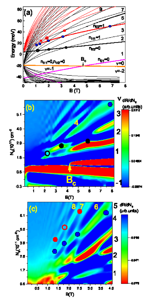
The spectrum in Fig. 5 (a) has four (in contrast to two in single QWs) special levels with zero LL index. Two of them (marked by the indices and ) originate from the heavy hole subbands, do not hybridize with other levels, and stay nearly degenerate at any , following a linear dependence . The splitting of peak in Fig. 5 (b) near the CNP at T is identified with the crossing between these levels and zeroth LL of E1 subband (the calculation gives T). The fact that the state with at negative still persists at can be explained if one assumes that application of the gate voltage not only shifts the density away from zero but also creates an internal asymmetry of the DQW structure that opens a gap between H1 and H2 subbands. The zero LLs of H1 and H2 subbands then have the spectra , where is roughly estimated as and equal to 4.3 meV per cm-2 (here is the static dielectric constant of HgTe and nm is the distance between the centers of the wells). With increasing negative density, the Fermi level at high magnetic fields first becomes pinned to and then shifts down towards , staying either within the region between these two levels or pinned to as long as cm-2 T-1 (note that the capacitance of a single LL is approximately cm-2 per Tesla). This behavior of the Fermi level is in accordance with the observed behavior of .
| (T) | (T) | (T) | |||
|---|---|---|---|---|---|
| 0 | 1 | 2 | 5.6 | 3.4 | 5.7 |
| 0 | 2 | 3 | 3.2 | 2.0 | 3.0 |
| 0 | 3 | 4 | 2.2 | 1.2⋆ | 1.8⋆ |
| 1 | 2 | 4 | 7.5 | 6.8 | 8.6 |
| 1 | 3 | 5 | 3.8 | 3.1 | 4.3 |
| 1 | 4 | 6 | 2.3 | 2.0 | 2.7 |
| 1 | 5 | 7 | 1.8 | 1.3 | 1.9 |
| 1 | 6 | 8 | 1.35 | 1.05 | 1.8 |
| 2 | 4 | 7 | 2.5 | 3.25 | 4.5 |
| 2 | 5 | 8 | 1.8 | 1.85⋆ | 2.7⋆ |
| 2 | 6 | 9 | 1.37 | 1.35 | 1.9 |
| (T) | (T) | ||||
| 0 | 2 | 3 | 3.5 | 5.8 | |
| 0 | 3 | 4 | 2.6 | ||
| 0 | 4 | 5 | 2.2 | 2.9 | |
| 0 | 5 | 6 | 1.7 | 2.3 | |
| 1 | 3 | 5 | 4.5 | 7.9 | |
| 1 | 4 | 6 | 3.2 | 4.7 | |
| 1 | 5 | 7 | 2.5 | 3.6 | |
| 1 | 6 | 8 | 1.8 | 2.7 | |
| 1 | 7 | 9 | 1.45 | 2.25 | |
| 2 | 5 | 8 | |||
| 2 | 6 | 9 | 2.4 | 3.7 | |
| 2 | 7 | 10 | 1.9 | 2.9 | |
| 3 | 6 | 10 | 3.1 | 5.05 | |
| 3 | 7 | 11 | 2.15 | 4.05 |
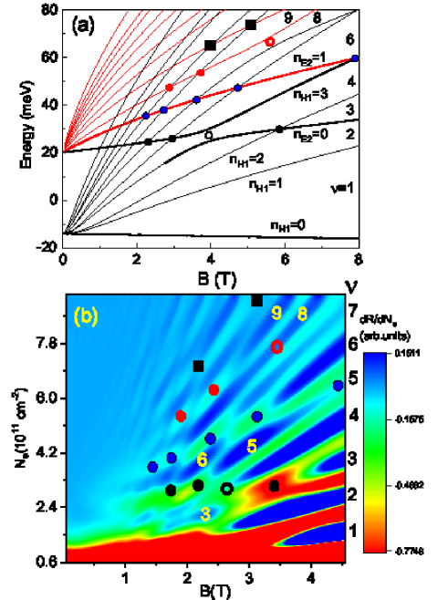
Figure 6 shows the theoretical LL spectra and experimental map for the DQW structure with nm. Since the resistance behavior in zero magnetic field reveals the presence of a gap meV at CNP, we have calculated the spectra by assuming an asymmetry caused by the electrostatic potential with the field kV/cm, which produces meV at . This leads to splitting of the zero LLs by already at , so the conduction and the valence bands are separated. Here we describe the LLs only in the conduction band. Except for the shift of the subbands and crossing points, the picture of the spectrum is similar to that of Fig. 5 (a). However, the electric field leads to a superlinear dispersion of the H1 subband LL energies at small , while in asymmetric DQWs with larger and the dispersion can even become non-monotonic. The resistance map again demonstrates a rich diamond-shaped pattern that qualitatively correlates with the calculated fan chart. Notice that the experimental map does not show a well-defined resistance maximum in the place where the anticrossing of LLs due to tunnel coupling is expected from the theory (open circle), in contrast to the places of true crossing (filled circles), and a similar behavior is seen in Fig. 5 (b), confirming the consistence between experiment and theory.
The positions of some important LL crossing points for both DQWs are summarized in the Tables II and III. Though the theory allows us to identify each of the main crossings observed, there is a lack of quantitative agreement between experimental and theoretical values of the corresponding magnetic fields. One of the reasons of this disagreement is the presence of the transverse field induced by the gate, which is not taken into account in the calculations. Since this field depends on the filling factor, a more precise description of LL spectrum requires a self-consistent approach, which is beyond the scope of this paper. Another important reason is related to possible measurement errors in determination of well widths and barrier thicknesses by the ellipsometry method. Indeed, the positions of crossing points, especially the ones involving level, are strongly sensitive to the barrier thickness , because a variation of strongly changes the tunnel-hybridization gap between E1 and E2 states thereby affecting the relative position of E2 subband with respect to H1 one. In particular, taking nm, which corresponds to four monolayers of Cd0.65Hg0.35Te, we obtain a better agreement between experiment and theory for the gapless DQW, as shown in Table 2. Finally, one should mention limitations of Kane model in application to heterostructures with narrow (several monolayers) potential barriers. A lack of quantitative agreement between experiment and theory in determination of LL positions in HgTe DQWs has been also pointed out by the other authors bovkun .
IV Conclusions
We have studied transport properties of the 2D fermion systems in HgTe-based DQWs in both gapless semimetal and gapped topological insulator phases in the presence of a perpendicular magnetic field. By changing independently the electron density and the magnetic field, we have observed multiple crossing of LLs originating from different subbands, according to earlier theoretical predictions kristopenko . The data indicates a similarity of the energy spectrum of gapless HgTe DQWs to that of bilayer graphene. However, in contrast to bilayer graphene, the separation of subbands in such structures is small, which allowed us to observe numerous crossigns at relatively low densities. In the charge neutrality point, we have indicated a special crossing of zeroth LLs, which is a hallmark of topologically non-trivial materials described by the Dirac-like BHZ Hamiltonian konig . The pattern of the crossing points in both kinds of HgTe DQWs generally correlates with the theoretical picture of energy spectrum of LLs. The reasons for deviations of the experimental crossing points from the theoretical ones are discussed.
It is expected that a symmetric HgTe DQW in the gapless semimetal phase can be switched electrically to the 2D topological insulator state as a gap between heavy hole subbands H1 and H2 opens in the presence of a transverse electric field. By observing the behavior of the resistance at low filling factors, we have obtained an indirect evidence that application of the bias to a single (top) gate not only changes the density but also opens the gap. An independent control of the energy spectrum and electron density can possibly be achieved with the use of double gating technology, which is still missing for MBE-grown HgTe DQWs. This may become useful for a more precise evaluation of the parameters which determine the energy spectrum. The double gating can also enable the exploration of the quantum Hall ferromagnetism in Dirac materials and development of electrically tunable topological insulators in multilayer HgTe-based systems.
ACKNOWLEDGEMENTS
The financial support of this work by RFBI Grant No. 18-02-00248a., FAPESP (Brazil), and CNPq (Brazil) is acknowledged.
References
- (1) M. Konig, S. Wiedmann, C. Brune, A. Roth, H. Buhmann, L. W. Molenkamp1, X.-L. Qi, and S.-C. Zhang, Science 318, 766 (2007).
- (2) B. A. Bernevig and S. C. Zhang, Phys. Rev. Lett. 96, 106802 (2006); B. A. Bernevig, T. L. Hughes, and S. C. Zhang, Science 314, 1757 (2006).
- (3) M. Z. Hasan and C. L. Kane, Rev. Mod. Phys. 82, 3045 (2010); X-L. Qi and S.-C. Zhang, Rev. Mod. Phys. 83, 1057 (2011).
- (4) X.-L. Qi and S.-C. Zhang, Phys. Today 63, 33 (2010).
- (5) C. L. Kane and E. J. Mele, Phys. Rev. Lett. 95, 146802 (2005); C. L. Kane and E. J. Mele, Phys. Rev. Lett. 95, 226801 (2005).
- (6) J. E. Moore and L. Balents, Phys. Rev. B 75, 121306(R) (2007).
- (7) J. E. Moore, Nature (London) 464, 194 (2010).
- (8) B. Zhou, H.-Z. Lu, R.-L. Chu, S.-Q. Shen, and Q. Niu, Phys. Rev. Lett. 101, 246807 (2008).
- (9) A. Roth, C. Brune, H. Buhmann, L. W. Molenkamp, J.Maciejko, X.-L. Qi, and S.-C. Zhang, Science 325, 294 (2009).
- (10) G. M. Gusev, Z. D. Kvon, O. A. Shegai, N. N. Mikhailov, S. A. Dvoretsky and J. C. Portal, Phys. Rev. B 84, 121302(R) (2011).
- (11) B. Büttner, C. X. Liu, G. Tkachov, E. G. Novik, C. Brüne, H. Buhmann, E. M. Hankiewicz, P. Recher, B. Trauzettel, S. C. Zhang, and L. W. Molenkamp, Nat. Phys. 7, 418 (2011).
- (12) D. A. Kozlov, Z. D. Kvon, N. N. Mikhailov, and S. A. Dvoretskii, JETP Lett. 96, 730 (2012).
- (13) G. M. Gusev, D. A. Kozlov, A. D. Levin, Z. D. Kvon, N. N. Mikhailov, and S. A. Dvoretsky, Phys. Rev. B, 96, 045304 (2017).
- (14) P. Michetti, J. C. Budich, E. G. Novik, and P. Recher, Phys. Rev. B, 85, 125309 (2012).
- (15) S. S. Krishtopenko, W. Knap, and F. Teppe, Nat. Sci. Rep. 6, 30755 (2016).
- (16) A. H. Castro Neto, F. Guinea, N. M. R. Peres, K. S. Novoselov, and A. K. Geim, Rev. Mod. Phys. 81, 109 (2009).
- (17) Edward McCann, Phys. Rev. B 74, 161403(R) (2006).
- (18) G. M. Gusev, E. B. Olshanetsky, F. G. G. Hernandez, O. E. Raichev, N. N. Mikhailov, and S. A. Dvoretsky, Phys. Rev. B 101, 241302(R) (2020).
- (19) N. M. R. Peres, Rev. Mod. Phys. 82, 2673 (2010).
- (20) S. Das Sarma, S. Adam, E. H. Hwang, and E. Rossi, Rev. Mod. Phys. 83, 407 (2011).
- (21) E. McCann and V. I. Fal’ko, Phys. Rev. Lett. 96, 086805 (2006).
- (22) J. Nilsson, A. H. Castro Neto, F. Guinea, and N. M. R. Peres, Phys. Rev. Lett. 97, 266801 (2006).
- (23) M. Koshino and E. McCann, Phys. Rev. B 81, 115315 (2010).
- (24) L. M. Zhang, M. M. Fogler, and D. P. Arovas, Phys. Rev. B 84, 075451 (2011).
- (25) T. Taychatanapat, K. Watanabe, T. Taniguchi, and P. Jarillo-Herrero, Nat. Phys. 7, 621 (2011).
- (26) P. Stepanov, Y. Barlas, T. Espiritu, S. Che, K. Watanabe, T. Taniguchi, D. Smirnov, and C. N. Lau, Phys. Rev. Lett. 117, 076807 (2016).
- (27) B. Datta, S. Dey, A. Samanta, H. Agarwal, A. Borah, K. Watanabe, T. Taniguchi, R. Sensarma, and M. M. Deshmukh, Nat. Commun. 8, 14518 (2017).
- (28) A different kind of LL crossing, however, exists in the twisted bilayer graphene due to splitting of the states of the upper and lower layers in the momentum space, T.-F. Chung, Y. Xu, and Y. P. Chen, Phys. Rev. B 98, 035425 (2018).
- (29) Z. Papic, D. A. Abanin, Y. Barlas, and R. N. Bhatt, Phys. Rev. B 84, 241306(R) (2011).
- (30) M. V. Yakunin, S. S. Krishtopenko, S. M. Podgornykh, M. R. Popov, V. N. Neverov, N. N. Mikhailov, and S. A. Dvoretsky, JETP Lett. 104, 403 (2016); S. M. Podgornykh, M. V. Yakunin, S. S. Krishtopenko, M. R. Popov, N. N. Mikhailov, and S. A. Dvoretskii, Semiconductors 53, 919 (2019).
- (31) L. S. Bovkun, S. S. Krishtopenko, A. V. Ikonnikov, V. Ya. Aleshkin, A. M. Kadykov, S. Ruffenach, C. Consejo, F. Teppe, W. Knap, M. Orlita, B. Piot, M. Potemski, N. N. Mikhailov, S. A. Dvoretskii, and V. I. Gavrilenko, Semiconductors 50, 1532 (2016); L. S. Bovkun, A. V. Ikonnikov, V. Ya. Aleshkin, K. V. Maremyanin, N. N. Mikhailov, S. A. Dvoretskii, S. S. Krishtopenko, F. Teppe, B. A. Piot, M. Potemski, M. Orlita, and V. I. Gavrilenko, Opto-Electronics Rev. 27, 213 (2019).
- (32) G. M. Gusev, E. B. Olshanetsky, Z. D. Kvon, and N. N. Mikhailov, Sol. St. Commun. 302, 113701 (2019).
- (33) O. E. Raichev, Phys. Rev. B 85, 045310 (2012).
- (34) E. G. Novik, A. Pfeuffer-Jeschke, T. Jungwirth, V. Latussek, C. R. Becker, G. Landwehr, H. Buhmann, and L. W. Molenkamp, Phys. Rev. B 72, 035321 (2005).
- (35) C. Brüne, C. X. Liu, E. G. Novik, E. M. Hankiewicz, H. Buhmann, Y. L. Chen, X. L. Qi, Z. X. Shen, S. C. Zhang, and L. W. Molenkamp, Phys. Rev. Lett. 106, 126803 (2011).
- (36) O. E. Raichev, G. M. Gusev, E. B. Olshanetsky, Z. D. Kvon, N. N. Mikhailov, S. A. Dvoretsky, and J. C. Portal, Phys. Rev. B 86, 155320 (2012).
- (37) P. Maher, L. Wang, Y. Gao, C. Forsythe, T. Taniguchi, K. Watanabe, D. Abanin, Z. Papic, P. Cadden-Zimansky, J. Hone, P. Kim, and C. R. Dean, Science 345, 61 (2014).
- (38) D. A. Abanin, K. S. Novoselov, U. Zeitler, P. A. Lee, A. K. Geim and L. S. Levitov, Phys. Rev. Lett. 98, 196806 (2007).
- (39) J. Velasco Jr, L. Jing, W. Bao, Y. Lee, P. Kratz, V. Aji, M. Bockrath, C. N. Lau, C. Varma, R. Stillwell, D. Smirnov, F. Zhang, J. Jung, and A. H. MacDonald, Nat. Nanotechnol. 7, 156 (2012).
- (40) R. T. Weitz, M. T. Allen, B. E. Feldman, J. Martin, and A. Yacoby, Science 330, 812 (2010).
- (41) K. Lee, B. Fallahazad, J. Xue, D. C. Dillen, K. Kim, T. Taniguchi, K. Watanabe, and E. Tutuc, Science 345, 58 (2014).