Tunneling study in granular aluminum near the Mott metal-to-insulator transition
Abstract
We find excellent agreement between tunneling and optical conductivity gap values in superconducting granular aluminum films, up to the metal-to-insulator transition. This behavior, in strong contrast with that recently reported in atomically disordered samples for which the optical gap becomes smaller than the tunneling gap, suggests that disorder is not at the origin of the transition. The large increase seen in the strong coupling ratio and a finite value of the gap at near the metal-to-insulator transition are consistent with a BCS to BEC crossover.
I Introduction
In conventional BCS theory [1] the superconducting gap in the density of states (DOS) is equal to half of the absorption threshold for photons . This statement remains correct for the case of a mildly disordered dirty superconductor (SC) [2], i.e. where is the Fermi energy, is the Fermi wave vector and is the mean free path, far from a disorder driven Anderson metal-to-insulator (M/I) transition. In that case, the BCS based Mattis-Bardeen (MB) theory [3] describes the frequency dependent complex optical conductivity exceptionally well. Its real part drops to zero below . It has a minimum at that frequency at finite temperatures.
When disorder on the atomic scale is increased, Larkin and Ovchinnikov (LO) theory predicts that the coherence peak in the DOS located at broadens. It has a universal shape which depends on a single parameter that increases with disorder. As it does, the absorption threshold becomes smaller than the mean value of the gap given approximately by the location of the maximum in the DOS [4]. The DOS will differ from the BCS prediction and the optical conductivity will not follow the MB theory. The energy scale as determined by optical conductivity will become smaller than the energy scale as determined by tunneling. In the case that the system is composed of metallic grains weakly coupled together, disorder consists of the broad distribution of the grain size and the coupling between the grains. In that case as well, the gap will be inhomogeneous resulting in similar differences between optical and tunneling gap measurements.
If one assumes that the system is homogeneous, the gap should be homogeneous as well. Determinations of the gap by optical and tunneling measurements should give the same results. The insulating state can be driven by the competition between the bandwidth and the Coulomb interaction i.e., a M/I transition of the Mott type.
Experiments on atomically disordered SCs such as InOx and NbNx show indeed that as disorder increases, indeed becomes smaller than [5, 6]. In the case of NbNx, the experiment is consistent with the LO theory [6].
In this work we present a study of granular aluminum (grAl) films approaching the M/I transition using planar tunneling junctions. We find that in these films, consisting of nano-scale metallic grains weakly coupled together, the tunneling energy scale and the optical energy scale [7] remain equal to each other up to the M/I transition. This implies that disorder plays only a minor role in the M/I transition of grAl, contrary to the case of NbNx and InOx. We ascribe this different behavior to a M/I transition, triggered by the electrostatic charging energy of the small grains. In that case the M/I transition is expected to be of the Mott type [8, 7, 9, 10] rather than an Anderson type as seen in atomically disordered films. According to dynamical mean field theory (DMFT) calculations, in a Mott transition a narrow region of finite and unchanged DOS relatively to the metallic state is formed at the Fermi level [11]. Hence, a BCS-BEC crossover is expected as the width of this region approaches the superconducting gap. In that scenario there is no known reason why the energy scales and should become different.
Rather, in the smooth crossover from highly overlapping fermionic pairs () to tightly bound bosonic molecules (), it is the energy scales (the pairing energy) and (the condensation temperature) that are progressively decoupled from each other [12]. In the BCS side they are linked by the weak-coupling relation while in the so called unitary limit where (near the BEC side) this ratio is increasing up to about 6 [13, 14]. It is precisely this behavior that we have observed.
II Methods
The grAl films were prepared by thermally evaporating clean Al pellets under controlled O2 pressure onto liquid nitrogen cooled substrate or onto room temperature warm substrate, for more details see [7]. The role that the substrate temperature plays is crucial, since it determines the grain size, its distribution and the maximum . For substrates held at room temperature the maximum is about 2.2 K [15, 16, 17] and the grain size is about nm [18] whereas for substrates held at liquid nitrogen temperature the maximum is about 3.2 K and the grain size is about nm [15, 19].
In order to obtain samples with varying normal state resistivity along the phase diagram we varied the O2 pressure while keeping the deposition rate around . To obtain high quality, homogeneous samples (in the sense of grain coupling), we made sure that the pressure and deposition rate were stable during deposition.
For the tunneling experiments we first evaporate 50 nm of grAl film onto liquid nitrogen cooled Al2O3 substrate, patterned to a rectangle with dimensions of 0.5x4 mm, by using a hard mask. After evaporation, we expose the film to atmosphere for a few hours, resulting in a native thin oxide barrier. We then use a second mask to evaporate two 50 nm thick, 0.5 mm wide aluminum strips, perpendicular to the grAl film, resulting in a grAl-oxide-Al tunneling junctions. In addition, this geometry allows us to measure the resistivity of the film vs. temperature and therefore to determine the critical temperature and the normal state resistivity for each sample.
For each junction we took current-voltage (I vs. V) and differential conductance-voltage (dI/dV vs. V) characteristics using Keithley 6221 current source and Keithley 2182A nano-voltmeter, operated in differential conductance mode. The same set of equipment, operated in delta mode, was used for the resistivity measurements. Measurements were taken in three different systems: a commercial 3He probe by Quantum Design PPMS with a base temperature of 0.4 K, commercial Oxford Instruments Triton 400 dilution refrigerator with a base temperature of ~20 mK and a liquid 4He bath cryostat with a base temperature of about 1.5 K.
Each dI/dV spectrum was fitted to a standard tunneling form [20]
| (1) |
where is the Fermi function, is the constant density of states (DOS) of the Al electrode and is the Dynes DOS [21] that takes into account the coherence peaks broadening . This approach allows us to obtain the superconducting gap and the broadening parameter . For the highest resistivity sample studied we have normalized the data prior to fitting it with Eq. 1 in order to avoid the influence of the high voltage behavior [22, 23] on the superconducting DOS. For more details on the data analysis, see supplemental material [24].
To extend the comparison between tunneling and optical conductivity to samples having larger grain size, additional samples were prepared on mm3 MgO or mm3 (LaAlO3)0.3- (SrAl0.5Ta0.5O3)0.7 (LSAT) substrates, held at room temperature, for THz optical spectroscopy. All samples are 100 nm thick, except the lowest resistivity one, which is 40 nm thick. Measurements were done by utilizing a quasi-optical Mach-Zehnder interferometer with backward-wave oscillators (BWO) in a frequency range of 3-17 cm-1 (or about 0.1-0.5 THz). Commercial optical 4He cryostat with a home built sample holder, provides us dynamic temperature range down to 1.5 K. The complex transmission was measured for all samples at 4.2 K and at various temperatures close to and below down to 1.5 K. We then obtain the optical conductivity from the measured complex transmission function. We take at 4.2 K as the normal-state conductivity and then fit the resulted to Mattis-Bardeen (MB) theory [3], as appropriate for a dirty limit SC [25, 7]. The only fitting parameter is which we fit to the BCS gap equation [1] in order to obtain . For more details, see supplemental material [24]. We used Dynes et al. [16] tunneling data for samples prepared under similar conditions, in order to compare between the optical and tunneling gaps of the larger grain size samples.
III Results
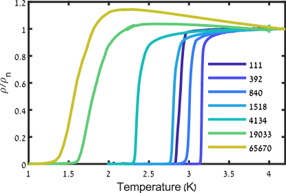
The resistivity curves for selected 2 nm grain samples are shown in Fig. 1. We take as the temperature where the resistivity falls to one percent of its normal state value. Tunneling differential conductance data for samples having a resistivity value up to ~1500 was taken from down to ~1.6-1.8 K, above the critical temperature of the Al counter-electrode. We note that for a few measured junctions was found to be ~0.1 meV and roughly temperature independent, in contrast to all other samples showing a decreasing with temperature (see for example Figs. S4 and S5 in the supplemental material [24]). We find this as an indication that for these samples the barrier quality is poor and therefore we have discarded their values. We note that for samples where near and below (see Fig. 6 and Fig. S4) the reliability of the obtained values from the fit is low.
The zero temperature value of the gap was determined by fitting to the BCS gap equation [1]. For samples having very high resistivity values approaching the Metal to Insulator transition, and substantially reduced critical temperatures, tunneling data was also taken at lower temperatures down to 30 mK. In that case data was taken both in zero field, and in a magnetic field of ~0.1 T, high enough to quench superconductivity in the Al counter-electrode.
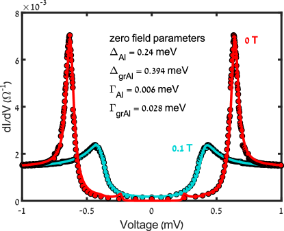
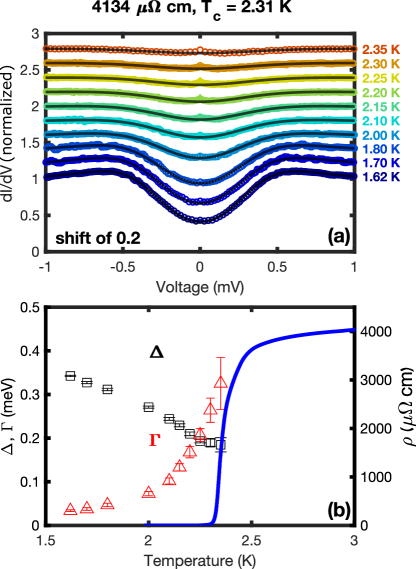
We observed a few percent change in the gap relatively to its zero field extrapolated value up to a field of 1 Tesla. The change in the value of with increasing magnetic field is more significant, as expected since it introduces spatial inhomogeneities in the gap due to the normal cores of about 6-7 nm in size [10] (see supplemental material for more details [24]). The orbital upper critical field is estimated as about 4 T as measured in a previous work on similar samples [10]. We therefore conclude that the applied field of ~0.1 T does not significantly affect the measured DOS of the grAl film. We show in Fig. 2 the tunneling data for a sample having a resistivity value of ~4,000 measured at 30 mK, both in zero applied field and 0.1 T applied field. Both sets have been fitted to a Dynes form, in zero applied field taking for the Al counter-electrode a gap of 0.24 meV and for the grAl film a gap of 0.394 meV extrapolated down to zero field (full field dependent analysis can be found in the supplemental material [24]). A similar analysis was performed on a ~66,000 sample at 0.4 K, resulting in a gap of 0.26 meV for the Al counter electrode with the grAl film having a gap of 0.32 meV, even though its critical temperature of 1.37 K is lower than the one measured for the Al counter electrode of 1.78 K. More details can be found in the supplemental material [24].
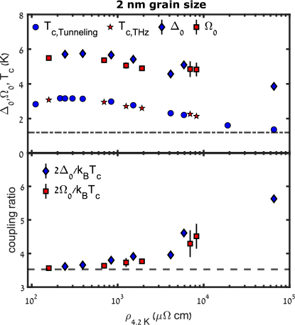
Tunneling gap values for 2 nm grain size samples having resistivity values ranging from ~100 to ~66,000 are shown in Fig. 3 where they are compared to optical gap values for samples having resistivity values up to ~8000 . It can be clearly seen that they both sets are in excellent agreement. This point is further illustrated in Fig. 4, where as indicated by the coherence peak position for the tunneling data and by the minimum in for the optical data are seen to coincide. We note that the decrease of at high resistivity values is substantially weaker than that of the critical temperature. As shown in Fig. 3, the trend of increasing strong coupling ratio previously reported for the optical gap [25, 7] can be clearly seen here. It reaches a value of 5.64 for the ~66,000 cm sample.
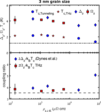
We can gain more insight on the role of the grain size by making a similar comparison between optical and tunneling data for samples with a grain size of 3 nm. We have compared as measured from the optical conductivity data (see supplemental material [24]) to the tunneling as measured by Dynes et al. [16], see top panel of Fig. 5. As for the case of 2 nm grain size samples, there is good agreement between the tunneling and optical conductivity gaps. As well, the variation of is in line with the tunneling data. However, we see that the coupling ratio (Fig. 5, bottom panel) does not change as rapidly in comparison to the 2 nm grain size samples. It does however reach a value close to 5 for the highest resistivity sample.
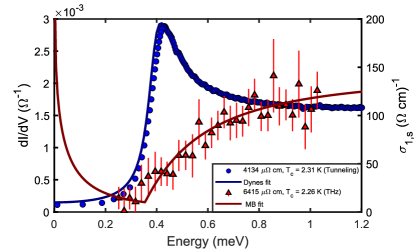
Besides the anomalously large values of the strong coupling ratio seen in high resistivity samples, a closer look at their tunneling data near reveals that their gap is not being fully closed, as it should in a conventional SC. We have observed such behavior for resistivity values above ~800 cm, within a temperature range which increases with sample resistivity (see supplemental Fig. S4 [24]). This behavior is well demonstrated in Fig. 6 for the ~4,000 cm sample. Quite near its gap is still around 0.3 meV, while at low temperature it reaches 0.394 meV, see Fig. 2.
IV Discussion
In atomically disordered SC, the M/I transition is of the Anderson type. As disorder increases, the tunneling and optical conductivity gaps are being progressively separated, as was observed in NbNx [26, 28, 27, 6, 5] and InOx [29, 5]. The separation can be described quite well by the theory of LO [4] which predicts that , where is a depairing parameter that increases with disorder. This theory shows good agreement with experiment [6]. This is in strike contrast to what we observe in grAl, namely there is a good agreement between the tunneling and optical conductivity gaps up to very high resistivity values, much higher than observed in NbNx. The work of Feigel’man and Skvortsov [30] confirms that strong disorder should manifest itself as a different tunneling and optical gaps. They predict that in that case the parameter should not be small compared to the gap. We have compared values of to the differential conductance peak position and found it to be small even up to resistivities of several 1,000 cm. Therefore, disorder effects are small in our case and plays little role, if any, in the M/I transition of grAl. Recent scanning tunneling microscope (STM) measurements on samples prepared on room temperature substrates shows that the gap value does not change within the sample [31], a clear sign for low disorder.
Rather our two central results: the large increase of the strong coupling ratio and the anomalous behavior of the gap near , point out to a different interpretation: a BCS-BEC cross-over as the M/I transition is approached. We find remarkable that for our highest resistivity 2 nm grain size sample, which is very close to being insulating, the value close to 6 that we have obtained for the strong coupling ratio is that predicted at cross-over [13, 14]. We also note that a similar value (about 5) is obtained from tunneling data of Dynes et al. for a 3 nm grain size sample having a very close resistivity value [16]. A non-closure of the gap at , as can be seen in Fig. 6, is also expected at a BCS to BEC cross-over. This is because of the different nature of excitations leading to the destruction of superconductivity in the BCS and BEC regimes: pair breaking in the former, collective excitations in the latter. At cross-over pair formation already occurs above .
A Mott transition has been shown to occur in granular aluminum films having a resistivity of about 50,000 cm at room temperature [8], very close to that of our highest resistivity sample where the largest strong coupling ratio is seen (having a room temperature resistivity of about 20,000 cm). A Mott driven BCS to BEC crossover thus provides an explanation for our observations. It can be expected that the split between a lower and a higher Hubbard bands with a narrow DOS peak subsisting in the middle, predicted by DMFT theory [11], should impact the tunneling conductance near a Mott transition. However, the absence of a tunneling theory for that regime does not allow at this point a quantitative analysis of the tunneling data. In addition, recent calculations of a model that takes into account both Mott behavior and SC shows as well that the coupling ratio exceeds that of the BCS weak coupling value [32]. Another piece of evidence which supports this picture is the fact that the coherence length decreases with resistivity down until it saturates to a value of about 6-7 nm (as obtained from upper critical field measurements [10]). This saturation of the coherence length is a characteristic of the BCS-BEC crossover regime [33].
In conclusion, we have measured the evolution of the SC gap by tunneling and THz spectroscopy in granular aluminum films, and have found them to be in good agreement up to the vicinity of the M/I transition. We have shown that the coupling ratio is increasing up to about 6 for 2 nm grain size samples, and that as the transition is approached there is no closure of the gap at . Both features are characteristic of a BCS-BCS crossover, which we have proposed is induced by the vicinity to a Mott transition. A quantitative analysis of the tunneling data, in particular regarding the behavior of the conductance near for high resistivity samples, is needed to bring a definite proof of a BCS-BEC crossover. This requires a tunneling theory for that regime that is not yet available.
Acknowledgments
Helpful discussions with Ioan Pop and Giancarlo Strinati are gratefully acknowledged. We thank Yoram Dagan for granting us access to his dilution refrigerator.
References
- Bardeen et al. [1957] J. Bardeen, L. N. Cooper, and J. R. Schrieffer, Phys. Rev. 108, 1175 (1957).
- Anderson [1959] P. W. Anderson, Journal of Physics and Chemistry of Solids 11, 26 (1959).
- Mattis and Bardeen [1958] D. C. Mattis and J. Bardeen, PR 111, 412 (1958).
- Larkin and Ovchinnikov [1972] A. Larkin and Y. N. Ovchinnikov, Sov. Phys. JETP 34, 1144 (1972).
- Sherman et al. [2015] D. Sherman, U. S. Pracht, B. Gorshunov, S. Poran, J. Jesudasan, M. Chand, P. Raychaudhuri, M. Swanson, N. Trivedi, A. Auerbach, M. Scheffler, A. Frydman, and M. Dressel, Nature Physics 11, 188 (2015).
- Cheng et al. [2016] B. Cheng, L. Wu, N. J. Laurita, H. Singh, M. Chand, P. Raychaudhuri, and N. P. Armitage, Phys. Rev. B 93, 180511 (2016).
- Moshe et al. [2019] A. G. Moshe, E. Farber, and G. Deutscher, Phys. Rev. B 99, 224503 (2019).
- Bachar et al. [2015] N. Bachar, S. Lerer, A. Levy, S. Hacohen-Gourgy, B. Almog, H. Saadaoui, Z. Salman, E. Morenzoni, and G. Deutscher, Phys. Rev. B 91, 041123 (2015).
- Glezer Moshe et al. [2020a] A. Glezer Moshe, E. Farber, and G. Deutscher, Appl. Phys. Lett. 117, 062601 (2020a).
- Glezer Moshe et al. [2020b] A. Glezer Moshe, E. Farber, and G. Deutscher, Phys. Rev. Research 2, 043354 (2020b).
- Georges et al. [1996] A. Georges, G. Kotliar, W. Krauth, and M. J. Rozenberg, Rev. Mod. Phys. 68, 13 (1996).
- Strinati et al. [2018] G. C. Strinati, P. Pieri, G. Ropke, P. Schuck, and M. Urban, Physics Reports 738, 1 (2018), the BCS - BEC crossover: From ultra-cold Fermi gases to nuclear systems.
- Pisani et al. [2018a] L. Pisani, P. Pieri, and G. C. Strinati, Phys. Rev. B 98, 104507 (2018a).
- Pisani et al. [2018b] L. Pisani, A. Perali, P. Pieri, and G. C. Strinati, Phys. Rev. B 97, 014528 (2018b).
- Deutscher et al. [1973a] G. Deutscher, M. Gershenson, E. Grunbaum, and Y. Imry, Journal of Vacuum Science and Technology 10, 697 (1973a).
- Dynes et al. [1984] R. C. Dynes, J. P. Garno, G. B. Hertel, and T. P. Orlando, Phys. Rev. Lett. 53, 2437 (1984).
- Levy-Bertrand et al. [2019] F. Levy-Bertrand, T. Klein, T. Grenet, O. Dupré, A. Benoît, A. Bideaud, O. Bourrion, M. Calvo, A. Catalano, A. Gomez, J. Goupy, L. Grünhaupt, U. v. Luepke, N. Maleeva, F. Valenti, I. M. Pop, and A. Monfardini, Phys. Rev. B 99, 094506 (2019).
- Deutscher et al. [1973b] G. Deutscher, H. Fenichel, M. Gershenson, E. Grunbaum, and Z. Ovadyahu, Journal of Low Temperature Physics 10, 231 (1973b).
- Lerer et al. [2014] S. Lerer, N. Bachar, G. Deutscher, and Y. Dagan, Phys. Rev. B 90, 214521 (2014).
- Tinkham [2004] M. Tinkham, Introduction to Superconductivity: Second Edition, Dover Books on Physics (Dover Publications, 2004).
- Dynes et al. [1978] R. C. Dynes, V. Narayanamurti, and J. P. Garno, Phys. Rev. Lett. 41, 1509 (1978).
- Dynes and Garno [1981] R. C. Dynes and J. P. Garno, Phys. Rev. Lett. 46, 137 (1981).
- Altshuler and Aronov [1979] B. Altshuler and A. Aronov, Solid State Communications 30, 115 (1979).
- [24] See Supplemental Material at […] for information on the THz spectroscopy and tunneling data analysis, and for additional data.
- Pracht et al. [2016] U. S. Pracht, N. Bachar, L. Benfatto, G. Deutscher, E. Farber, M. Dressel, and M. Scheffler, Phys. Rev. B 93, 100503 (2016).
- Chand et al. [2012] M. Chand, G. Saraswat, A. Kamlapure, M. Mondal, S. Kumar, J. Jesudasan, V. Bagwe, L. Benfatto, V. Tripathi, and P. Raychaudhuri, Phys. Rev. B 85, 014508 (2012).
- Mondal et al. [2011a] M. Mondal, A. Kamlapure, M. Chand, G. Saraswat, S. Kumar, J. Jesudasan, L. Benfatto, V. Tripathi, and P. Raychaudhuri, Phys. Rev. Lett. 106, 047001 (2011a).
- Mondal et al. [2011b] M. Mondal, M. Chand, A. Kamlapure, J. Jesudasan, V. C. Bagwe, S. Kumar, G. Saraswat, V. Tripathi, and P. Raychaudhuri, Journal of Superconductivity and Novel Magnetism 24, 341 (2011b).
- Sherman et al. [2014] D. Sherman, B. Gorshunov, S. Poran, N. Trivedi, E. Farber, M. Dressel, and A. Frydman, Phys. Rev. B 89, 035149 (2014).
- Feigel’man and Skvortsov [2012] M. V. Feigel’man and M. A. Skvortsov, Phys. Rev. Lett. 109, 147002 (2012).
- Yang et al. [2020] F. Yang, T. Gozlinski, T. Storbeck, L. Grünhaupt, I. M. Pop, and W. Wulfhekel, Phys. Rev. B 102, 104502 (2020).
- Phillips et al. [2020] P. W. Phillips, L. Yeo, and E. W. Huang, Nature Physics (2020).
- Spuntarelli et al. [2010] A. Spuntarelli, P. Pieri, and G. Strinati, Physics Reports 488, 111 (2010).