Geometric origins of topological insulation in twisted layered semiconductors
Abstract
Twisted bilayers of two-dimensional (2D) materials are proving a fertile ground for investigating strongly correlated electron phases. This is because the moiré pattern introduced by the relative twist between layers introduces long-wavelength effective potentials which lead to electron localization. Here, we develop a generalized continuum model for the electronic structure of moiré patterns, based on first-principles calculations and tailored to capture the physics of twisted bilayer 2D semiconductors. We apply this model to a database of eighteen 2D crystals covering a range of atomic relaxation and electronic structure features. Many of these materials host topologically insulating (TI) moiré bands in a certain range of twist angles, which originate from the competition between triangular and hexagonal moiré patterns, tuned by the twist angle. The topological phases occur in the same range as the maximally flat moiré bands.
Quantum materials, engineered by creative manipulation of the features of conventional crystals, offer new possibilities for breakthroughs in understanding electron correlations and superconductivity. What is intriguing is that these phenomena emerge at a length scale much larger than the underlying crystal lattice constant (by a factor of 10 to 1000), through features due to strain patterns, controlled by geometric constraints. A new platform for such studies are systems comprising few-layer two-dimensional (2D) crystals, like twisted bilayers of graphene or transition metal dichalcogenides (TMDCs) [1, 2, 3, 4, 5]. The slight lattice mismatch between two layers of a 2D material at a relative twist angle results in a moiré superlattice (MSL) and a long-wavelength periodic modulation of the effective electronic potential [6, 7]. In a narrow range of the twist angle, the moiré potentials act as confining wells for the electrons of the constituent monolayers, causing isolated flat bands and localized wave functions near the Fermi surface [8, 9].
In the moiré flat bands, the kinetic energy is heavily suppressed and electronic interactions play a dominant role, with the intensity of the interactions controlled by the twist angle; this effect has been dubbed “twistronics” [10]. Compared to twisted bilayer graphene (TBG), the twisted bilayer semiconductors can host flat bands in a large range of twist angles [11, 12] instead of at precisely a magic angle [1]. This makes it possible to overcome some experimental challenges in twisted bilayers of semiconductors; thus, the twist angle becomes an additional degree of freedom for fine-tuning other physical effects in the strongly correlated regime [13]. Intriguingly, topological insulator (TI) moiré bands were predicted in a twisted bilayer of MoTe2 [14]; this work introduced a possible candidate for observing concurrent correlated and TI phases in the same material.
It is difficult to model twistronic systems at small twist angles () using first-principles calculations, because the number of atoms in the MSL scales as . To overcome this limitation, continuum models with a low-energy effective Hamiltonian based on first-principles (density-functional theory, DFT) calculations were developed for electronic structures of TBG; this approach can accurately describe flat bands and magic angles [15, 9, 16, 17]. Although continuum models have also been applied to the twisted bilayer semiconductors [18, 14], they have yet to include the effect of atomic relaxations which play an important role at small angles [19, 20, 12, 11].
In this letter, we present results from a DFT-based generalized continuum method designed specifically for twisted bilayer semiconductors. The computed electronic structures are consistent with full-DFT results [12, 11, 2] but only require a relatively inexpensive set of bilayer calculations. These calculations involve systems with only a handful of atoms per unit cell, in contrast to the many thousands of atoms necessary in the calculation of a full MSL. We derive a database of relaxation and the corresponding coefficients of tight-binding electronic structure hamiltonians for eighteen materials with various lattice symmetries and band edge momenta. These coefficients do not capture the material’s entire band structure, but rather focus on the details of the parabolic band edges. Each layer contributes one band to the full twisted bilayer model, and these bands are coupled through a set of stacking-dependent electronic interactions.
In Fig. 1 we provide an overview of the different phases and their geometric origins, as the twist angle is changed in a moiré bilayer (Fig. 1a). The full interaction between the bands can be decomposed into two complementary parts. The first describes the tendency for electrons in one layer to tunnel to the other, as shown in Fig. 1b – labeled for “Tunneling”. The tunneling coefficients are strongest at (aligned) stacking regions and form a triangular (TR) lattice across the MSL. The second contribution captures the stacking dependence of the monolayer bands’ on-site energies, which depends on the electrostatic potential from the opposite layer, shown in Fig. 1c) – labeled and for “top/bottom” layer. The electrostatic potentials have maxima at the and stacking regions, forming a honeycomb (HC) lattice.
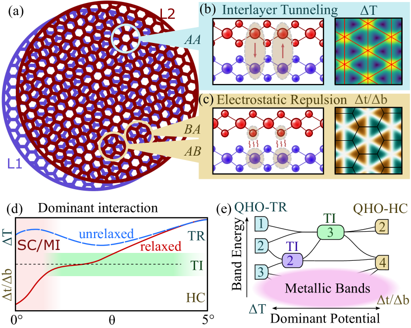
In the majority of materials studied here, the in-plane atomic relaxation of the twisted bilayers enhances the effects of the electrostatic potential fluctuations and reduces that of the interlayer tunneling, especially at small twist angles. Electron localization transitions, from the tunneling-dominated TR lattice to the electrostatic-dominated HC lattice, occur at low twist angle in various materials, as illustrated in Fig. 1d. In the low-angle region, ultra-flat moiré bands are predicted, likely to host superconducting (SC) and Mott insulating (MI) phases. The topologically insulating (TI) moiré bands appear for intermediate values of the twist angle, during the transition between the two types of lattice geometries for the interlayer electronic interactions (Fig. 1e). The electronic potentials naturally lead to quantum harmonic oscillator (QHO) states at small twist angles [21, 22, 23], whose presence underlies the appearance of the moiré flat bands and whose competition explains the large number of TI phases possible in twisted semiconductors.
We briefly introduce the methodology here. To capture the stacking-dependent electronic and atomic details, we perform DFT calculations on aligned bilayers over a grid sampling all possible interlayer displacements. Using the effective mass approximation, we treat the dispersion around the monolayer band extrema as a kinetic energy term in a continuum Hamiltonian. Including the three stacking-dependent potentials described in the introduction, we obtain the effective Hamiltonian:
| (1) |
where is the effective mass, are the electrostatic potentials for the top and bottom layer, and is the interlayer tunneling strength. At small twist angles we also include the all-important relaxation effects by minimizing the total mechanical energy of the moiré patterns [20]. The local electronic structures can then be derived from the DFT through the expansion:
| (2) |
To determine the from the local electronic structure, the Bloch wave functions at band extrema are extracted from DFT calculations to assess the layer polarization of each band. The moiré bands can then be calculated by diagonalizing the matrix form of the Hamiltonian for a truncated basis set in -space (see SM for details).
The aligned () stacking configuration has higher energy than the partially eclipsed (/) configuration for TMDCs and hBN homo-bilayers (). Consequently, relaxation tends to reduce the in-plane area of stacking region and to increase that of the / stacking region, thus minimizing the total energy [16, 20]. Upon relaxation, the large values of , at and stacking, expand to cover a larger area, while the peak regions of , at stacking, shrink, with relaxed structures showing stronger electrostatic potential effects and weaker tunneling effects, which causes a clear angle-dependent transition of the moiré electronic structure.
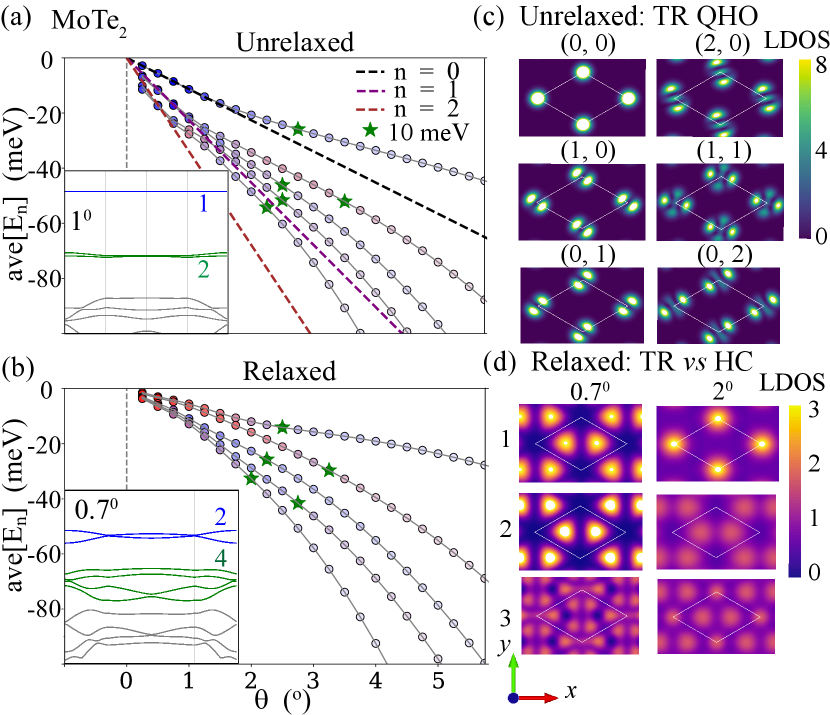
In Fig. 2a,b we present the angle-dependent bands and real-space localization of twisted bilayer MoTe2 as a representative case. The top-most valence bands for both the relaxed and unrelaxed moiré systems have a bandwidth less than 10 meV when the twist angle is below . Using the Coulomb repulsion energy () in TBG and twisted hBN as a guide [4, 11], this small kinetic energy implies that strongly correlated states could exist for any twist angle below a certain critical value in some TMDC materials [2, 24]. The relaxation effects drive the small-angle () valence moiré bands from TR-type to HC-type (Fig. 2). In the unrelaxed case, the band structure at shows a single uppermost flat band and a pair of flat bands under it, consistent with a stacking QHO model [21, 22]. The energy levels of the 2D TR QHO model are given by , , and the first three levels ,, and are accurately represented by the computed band averages for [21]. In contrast, a pair of top moiré bands and the four lower bands at correspond to the first () and second () QHO states, respectively of the HC lattice [22].
The real space localization of the tunneling-dominated (TR) QHO state is evident in the local density of states (LDOS) of the moiré bands for the unrelaxed condition, as shown in Fig. 2c. The electronic states localize around the stacking center and show s, p, and d-orbital distribution for the first three energy levels, respectively. The six moiré bands shown correspond to the QHO ground state, single excitation states (2-fold degenerate), and double excitation states (3-fold degenerate).
After relaxation, the competition between the two types of lattices is greatly altered, as shown in Fig. 2d. The two top bands in the low-angle case () localize in the / HC potential wells to from 2-fold degenerate ground states of the HC QHO model, while the third band is one of the 4-fold degenerate first excited states. In contrast, the localization of the uppermost band gradually changes to the stacking in the high-angle case () with the second band localized in the / region. This indicates that the energy level of the HC QHO model and the triangular QHO model cross as the angle changes, leading to a reordering of the bands’ localization. Therefore, the transition between the HC and TR electronic states can be controlled by varying the twist angle in the presence of atomic relaxations. The intermediate twist angles correspond to competing real-space distribution and band reordering, making these materials excellent candidates for hosting non-trivial topological properties.
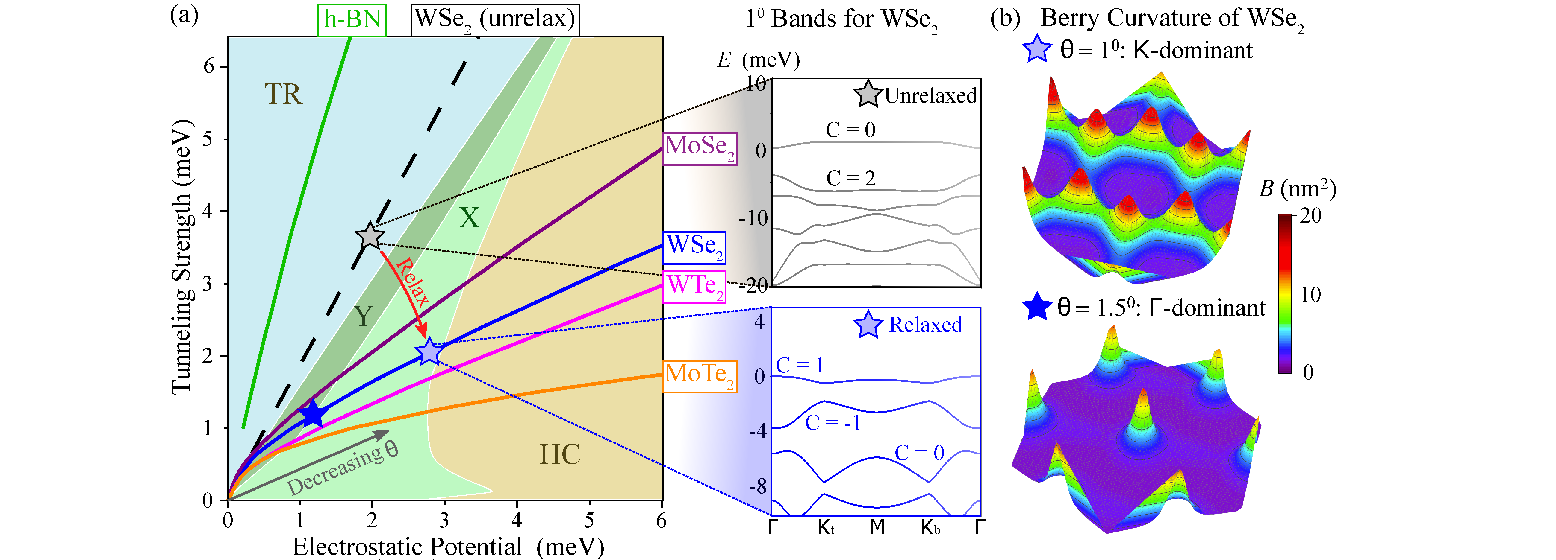
To study the topological properties associated with the TR-HC transition, we calculate the Chern numbers of the moiré bands for a generic twisted bilayer of a hexagonal semiconductor, and use these results to generate a TI phase diagram. The condition for the existence of topological bands is represented by the electrostatic potential and tunneling coefficients in Fig. 3a for a generic system, which are approximated by their first order Fourier coefficients labeled and , respectively. In this simplified model, the topological properties can be completely described by just two parameters, and , with the Hamiltonian
| (3) |
where is the lattice parameter, , , are the kinetic, potential, and tunneling energy, respectively, and , , are the material-independent quantities. The topologically trivial TR and HC phases appear in the -dominated and -dominated regions of the phase space of Fig. 3a, respectively. Interesting band structures occur in the intermediate region, which includes two types of topological non-trivial valence moiré bands. The Chern numbers of the three top-most moiré bands are (1, -1, 0) and (1, 1, -2) for X-type and Y-type topological insulators, respectively. Transitions between topological and trivial insulators for the uppermost band will occur on the boundary between the Y-type topological phase and TR phase where the top two bands overlap and then reopen, hosting protected edge modes at the transition. Similar topological transitions between the second and the third bands appears in the boundary between the X-type and Y-type topological phases. The transition on the boundary of the X-type topological phase and the HC phase is a TI-to-semimetal transition.
In Fig. 3a we show the curves in the phase diagram for 4 TMDC’s, indicating transitions between phases with increasing twist angle (without relaxation these curves would be straight lines like the one shown for WSe2). For comparison, we include the curve for hBN, which remains in one phase (TR) as it shows very weak relaxation. An explicit example of the topological transitions is also shown Fig. 3a for WSe2, including the unrelaxed case.
The band structures and Chern numbers of the bands confirm that the topological transition is primarily driven by atomic relaxation. In the unrelaxed 1 twisted WSe2, although the uppermost valence band is topologically trivial, the second valence band has a nonzero Chern number. The topological features of these lower valence bands are not reflected by the phase diagram, but we list them in our database for each material. In realistic experimental conditions, atomic-scale defects, bending, and local strain introduced during fabrication cause twisted bilayers to include different twist angles in different areas within a single sample [25]. Therefore, different domains of twist angle occur and introduce both topological and trivial bands. Topological edge states can appear along domain boundaries in the twist angle, according to the critical values in Tab. 1. These edge states would not be defined by a sharp change from one crystal to another, or from material to vacuum, but rather by slow variation in the twist angle. For this reason, these “internal” protected edge states would be excellent candidates for observing spin or valley-polarized states, as the only disorder comes from twist-angle variations, which are unlikely to induce a spin or valley swapping.
| Material | |||||
|---|---|---|---|---|---|
| MoSe2 | 0.9 | 1.4 | 2.4 | 2.98 () | 0.18 () |
| MoTe2 | 0.7 | 1.1 | 1.5 | 1.43 () | 0.30 () |
| WSe2 | 0.8 | 1.2 | 2.1 | 3.24 () | 0.19 () |
| WTe2 | 0.7 | 1.4 | 2.4 | 3.70 () | 0.18 () |
In Fig. 3b we show the Berry curvature of the uppermost valence band for two values of the twist angle. In the HC phase in the small-angle region, the first transition appears at where the two top bands separate at the MBZ’s points, indicated by the Berry curvature’s concentration there. With increasing twist angle, the Berry curvature of the top band gradually transfers to the point accompanied by an X/Y transition at . During this process, the topologically non-trivial top-most band takes on its minimal bandwith , meV, and its maximal topological band gap meV. At larger twist angle, the Berry curvature concentrates at the point during the transition to the TR phase, where the two top-most bands merge. The numerical results for the critical angles, maximal gap, and minimal band width for the TMDCs with topological valence bands are presented in Table 1. We have also verified that the bands and real space localization of MoS2 [12], WSe2 [2], and hBN [11] from our model are consistent with previous full DFT calculations. Twisted bilayers of WTe2 show the highest gap and one of the lowest bandwidths, making this material the best candidate for experimental study.
Including spin degrees of freedom, the spin-dependent moiré Hamiltonian decomposes into two copies [14]. At the valleys of the aligned bilayer, the two copies will be split by the spin-orbit coupling term, , which for most TMDCs is on the scale of meV, and the opposite spin-ordering will occur at the valley. The and points tend to have very weak spin-splitting, leading to two copies of the spin-independent Hamiltonian, as is the case in continuum treatments of twisted bilayer graphene [8]). However, as the two nonequivalent valleys are related by time reversal symmetry, the spin-up bands at valley and spin-down bands at valley have opposite Berry curvature and Chern numbers. Topologically non-trivial uppermost bands with opposite spin and Chern number give rise to the helical edge states protected by the TR symmetries at the boundaries, and could lead to observable quantum spin Hall (QSH) effects [26].
The origin of the TI phases has been ascribed [14] to a skyrmionic texture in the moiré potentials, which is an alternate interpretation of the TR/HC competition we presented here but captures the same key features. As the flatness of the bands causes stronger correlation effects, the topological phases in twisted bilayer semiconductors could exhibit the combination of TI and superconductivity, which has been the subject of an intense decades-long search for fractional statistics and Majorana fermions [26].
The generality of the relaxation-induced TI phases is partially explained by the connection between the stacking-dependence of the electronic structure and that of the ground state energy: the lowest stacking configuration of these materials seem to correspond to maxima of the electrostatic interaction and minima of the tunneling strength. We note that this trend might not be true across all 2D materials, and finding exceptions to the rule could be a valuable endeavor.
Acknowledgements.
We thank Ziyan Zhu and Daniel Larson for useful discussions. This work was supported by the National Science Foundation under grant No. OIA-1921199. The calculations in this work were performed in part on the FAS Research Computing cluster of Harvard University.References
- Cao et al. [2018a] Y. Cao, V. Fatemi, S. Fang, K. Watanabe, T. Taniguchi, E. Kaxiras, and P. Jarillo-Herrero, Nature 556, 43 (2018a).
- Wang et al. [2020] L. Wang, E.-M. Shih, A. Ghiotto, L. Xian, D. A. Rhodes, C. Tan, M. Claassen, D. M. Kennes, Y. Bai, B. Kim, et al., Nat. Mater. , 1 (2020).
- Yankowitz et al. [2019] M. Yankowitz, S. Chen, H. Polshyn, Y. Zhang, K. Watanabe, T. Taniguchi, D. Graf, A. F. Young, and C. R. Dean, Science 363, 1059 (2019).
- Cao et al. [2018b] Y. Cao, V. Fatemi, A. Demir, S. Fang, S. L. Tomarken, J. Y. Luo, J. D. Sanchez-Yamagishi, K. Watanabe, T. Taniguchi, E. Kaxiras, et al., Nature 556, 80 (2018b).
- Zondiner et al. [2020] U. Zondiner, A. Rozen, D. Rodan-Legrain, Y. Cao, R. Queiroz, T. Taniguchi, K. Watanabe, Y. Oreg, F. von Oppen, A. Stern, et al., Nature 582, 203 (2020).
- Lopes dos Santos et al. [2007] J. M. B. Lopes dos Santos, N. M. R. Peres, and A. H. Castro Neto, Phys. Rev. Lett. 99, 256802 (2007).
- Park et al. [2008] C.-H. Park, L. Yang, Y.-W. Son, M. L. Cohen, and S. G. Louie, Nat. Phys. 4, 213 (2008).
- Bistritzer and MacDonald [2011] R. Bistritzer and A. H. MacDonald, PNAS 108, 12233 (2011).
- Morell et al. [2010] E. S. Morell, J. Correa, P. Vargas, M. Pacheco, and Z. Barticevic, Phys. Rev. B 82, 121407 (2010).
- Carr et al. [2017] S. Carr, D. Massatt, S. Fang, P. Cazeaux, M. Luskin, and E. Kaxiras, Phys. Rev. B 95, 075420 (2017).
- Xian et al. [2019] L. Xian, D. M. Kennes, N. Tancogne-Dejean, M. Altarelli, and A. Rubio, Nano Lett. 19, 4934 (2019).
- Naik and Jain [2018] M. H. Naik and M. Jain, Phys. Rev. Lett. 121, 266401 (2018).
- Kerelsky et al. [2019] A. Kerelsky, L. J. McGilly, D. M. Kennes, L. Xian, M. Yankowitz, S. Chen, K. Watanabe, T. Taniguchi, J. Hone, C. Dean, A. Rubio, and A. N. Pasupathy, Nature 572, 95 (2019).
- Wu et al. [2019] F. Wu, T. Lovorn, E. Tutuc, I. Martin, and A. MacDonald, Phys. Rev. Lett. 122, 086402 (2019).
- Carr et al. [2019] S. Carr, S. Fang, Z. Zhu, and E. Kaxiras, Phys. Rev. Res. 1, 013001 (2019).
- Jung et al. [2014] J. Jung, A. Raoux, Z. Qiao, and A. H. MacDonald, Phys. Rev. B 89, 205414 (2014).
- Fang and Kaxiras [2016] S. Fang and E. Kaxiras, Phys. Rev. B 93, 235153 (2016).
- Wu et al. [2018] F. Wu, T. Lovorn, E. Tutuc, and A. H. MacDonald, Phys. Rev. Lett. 121, 026402 (2018).
- Nam and Koshino [2017] N. N. T. Nam and M. Koshino, Phys. Rev. B 96, 075311 (2017).
- Carr et al. [2018] S. Carr, D. Massatt, S. B. Torrisi, P. Cazeaux, M. Luskin, and E. Kaxiras, Phys. Rev. B 98, 224102 (2018).
- Carr et al. [2020] S. Carr, D. Massatt, M. Luskin, and E. Kaxiras, Phys. Rev. Res. 2, 033162 (2020).
- Angeli and MacDonald [2020] M. Angeli and A. H. MacDonald, arXiv e-prints (2020), arXiv:2008.01735 [cond-mat.str-el] .
- Naik et al. [2020] M. H. Naik, S. Kundu, I. Maity, and M. Jain, Phys. Rev. B 102, 075413 (2020).
- Zhang et al. [2020] Z. Zhang, Y. Wang, K. Watanabe, T. Taniguchi, K. Ueno, E. Tutuc, and B. J. LeRoy, Nature Physics 16, 1093 (2020).
- Uri et al. [2020] A. Uri, S. Grover, Y. Cao, J. A. Crosse, K. Bagani, D. Rodan-Legrain, Y. Myasoedov, K. Watanabe, T. Taniguchi, P. Moon, M. Koshino, P. Jarillo-Herrero, and E. Zeldov, Nature 581, 47 (2020).
- Qi and Zhang [2011] X.-L. Qi and S.-C. Zhang, Rev. Mod. Phys. 83, 1057 (2011).