Bath]Department of Physics, University of Bath, Bath BA2 7AY, United Kingdom Bath]Department of Physics, University of Bath, Bath BA2 7AY, United Kingdom Bath]Department of Physics, University of Bath, Bath BA2 7AY, United Kingdom Warwick]Department of Physics, University of Warwick, Coventry CV4 7AL, United Kingdom Bath]Department of Physics, University of Bath, Bath BA2 7AY, United Kingdom Bath]Department of Physics, University of Bath, Bath BA2 7AY, United Kingdom
Superconducting Quantum Interference in Twisted van der Waals Heterostructures
Abstract
Modern Superconducting QUantum Interference Devices (SQUIDs) are commonly fabricated from either Al or Nb electrodes, with an in-situ oxidation process to create a weak link between them. However, common problems of such planar nano- and micro-SQUIDs are hysteretic current-voltage curves, and a shallow flux modulation depth. Here, we demonstrate the formation of both Josephson junctions and SQUIDs using a dry transfer technique to stack and deterministically misalign flakes of NbSe2; allowing one to overcome these issues. The Josephson dynamics of the resulting twisted NbSe2-NbSe2 junctions are found to be sensitive to the misalignment angle of the crystallographic axes. A single lithographic process was then implemented to shape the Josephson junction into a SQUID geometry with typical loop areas of 25 and weak links 600 nm wide. These devices display large stable current and voltage modulation depths of up to 75 and 1.4 mV respectively.
Superconducting QUantum Interference Devices (SQUIDs) are key components in the development of ultra-sensitive electric and magnetic measurement systems.1 The basic SQUID design consists of a superconducting ring intersected by one (rf SQUID) or two (dc SQUID) Josephson junctions; the latter consisting of two superconducting electrodes coupled by weak links that allow the flow of supercurrent. The weak link can take a variety of forms including point contacts, physical constrictions, or heterostructures consisting of a thin normal metal or insulating barrier separating the two superconductors.2 The latter type is typically fabricated by deposition of metallic superconductors such as Al and Nb, with the tunnelling barrier formed by in-situ oxidation.3 This oxide barrier varies in thickness on the atomic scale and often contains defect traps, which can lead to highly non-uniform supercurrent distributions.4 In addition, over time oxygen atoms in the oxide barrier diffuse out, altering the normal state resistance of the junction resulting in a variation of the critical current, a process which can be detrimental to the longevity of the device.5 Since Josephson junctions are the basis of many superconducting technologies such as qubits,6 quantum metrology,7 and superconducting quantum interference devices (SQUIDs), development and incorporation of new materials with improved properties and functionality is vital.
An alternative route to the fabrication of oxide-free Josephson junctions is the stacking of two-dimensional materials (2D) into vertical van der Waals (vdW) heterostructures,8 a technique which holds promise for creating atomically clean and defect free interfaces. Additionally, vdW-based devices provide access to a new selection of superconducting materials such as Bi2Sr2CaCu2O8+δ,9 FeSe,10 and 2H-NbSe2.11. These materials all share a common characteristic in that they have a layered structure and easily cleave perpendicular to the -axis. These properties, along with the availability of dry transfer techniques,12 has allowed the fabrication of vdW heterostructure devices comprised of two or more mechanically exfoliated flakes. Such devices include junctions with dielectric tunnelling barriers,13, 14 superconducting-normal-superconducting Josephson junctions,15 and van der Waals interface Josephson junctions,16 which may prove useful in the formation of superconducting qubits.17 Furthermore, a vdW-based device offers an additional variable in the form of controlling the relative twist angle between the crystallographic axes of the two materials; a degree of freedom which is not available in conventional heterostructures. This twisting creates a misalignment between the two crystals, changing the atomic registry at the interface and leading to angular-dependent interlayer interactions. This enables one to tune the electronic coupling via the twist angle, leading to effects such as band hybridisation,18, 19 minigaps and band replicas due to scattering on moiré potentials,20 charge transfer and changes in effective masses 21, and has led to the discovery of a moiré superlattice in graphene/h-BN,22 as well as electrically tunable superconductivity in twisted bilayer graphene.23 This new field of study named twistronics, may prove valuable in the incorporation of two-dimensional materials into more complex vdW superconducting devices such as qubits and SQUIDs.
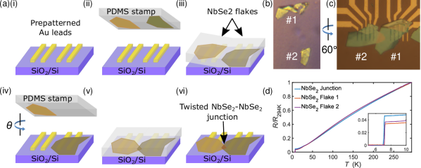
In this study, twisted NbSe2-NbSe2 heterostructures are formed by stacking two NbSe2 flake with a well-determined misalignment of the crystallographic axes using the procedure described in Methods and highlighted in Fig 1a. Briefly, two NbSe2 are sequentially stacked with a small overlap onto a Si/SiO2 substrate with pre-patterned Au contacts and encapsulated with a thin layer of hexagonal boron nitride. Typical junction areas are on the order of 20-60 m2 (Fig. 1c).
Before describing the characterisation of devices patterned with SQUID geometries, we investigate the transport properties of twisted NbSe2-NbSe2 junctions. The temperature-dependence of the normalised four-point resistance R(T)/R(294K) from 4 to 294 K is shown in Fig. 1d for two NbSe2 flakes with a relative twist angle of 60∘, as well as the resulting junction formed by the overlap region. We note that there is an uncertainty of 1∘ in the misalignment angle of devices arising from both the resolution of the rotation stage and unwanted movement of the PDMS during the stamping progress. Both flakes and junction show metallic transport behaviour which is phonon-limited at high temperature (R T) and disorder limited at low temperature (R approaches a constant value) before reaching the superconducting state at Tc 7 K.24 As the of NbSe2 is known to reduce in flakes 10 layers,13, 14 all flakes used were at least 10 nm, ensuring negligible suppression of . The residual resistance ratio (RRR), defined as R(T=294K)/R(T=8K), is found to be 30 for the two NbSe2 flakes, with a small variation due to the slightly different flake thicknesses. This is in contrast to the RRR of the junction region which is found to vary between 10-25 depending on the twist angle. A close up of the superconducting transition is shown in Fig 1(d), where it can be seen that the junction displays a slightly broader transition width when compared to the individual NbSe2 flakes, indicative of additional disorder at the interface.
0.0.1 Josephson junction performance
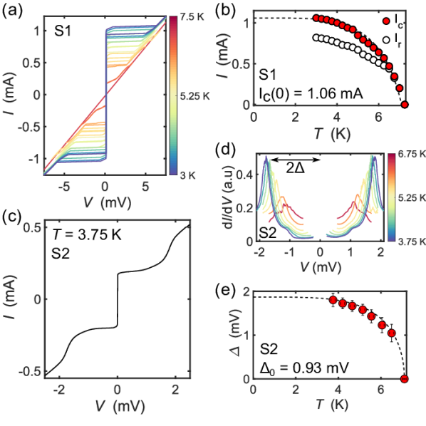
Next, we examine the current-voltage (I-V) characteristics of a NbSe2-NbSe2 junction for temperatures = 3 to 7.5 K (S1, Fig. 2a). Here the misorientation angle of the junction is estimated to be 6∘ from comparison of optical micrographs of the two flakes. From the presence of distinct retrapping currents in the I-V curves, it is clear that the junction behaviour is typical of an underdamped Josephson junction. This indicates that the vdW interface decouples the superconducting order parameters and creates a weak link that allows the flow of a Josephson supercurrent. Each NbSe2 flake has multiple electrical contacts, allowing the use of different voltage lead configurations to confirm that the bulk critical current of each flake is substantially larger than that of the junction. Next, we quantify the junction dynamics by examining the McCumber parameter , found by fitting the ratio between the retrapping current and the critical current and comparing it to a microscopic model.25 is found to be 0.89 at = 3 K, leading to a McCumber parameter 0.6, placing this device in the ’weakly underdamped’ category. Using the relationship the junction capacitance, , was found to be 1.6xF, yielding a specific capacitance of = 0.8 . Assuming the permittivity is that of vacuum, this leads to a gap between the two flakes of 1 nm, comparable to that of the -axis period in 2H-NbSe2 of 0.63 nm.
The temperature dependence of the critical current, , can be calculated using Ambegaokar-Baratoff (AB) theory26, in which is expressed as
| (1) |
where and are the zero temperature critical current and superconducting gap respectively. can be described by an interpolation approximation to the Bardeen-Cooper-Schrieffer (BCS) theory temperature-dependent superconducting energy gap,
| (2) |
The fit in Fig 2b shows that the critical current of sample S1 is reasonably well described by AB theory, in agreement with previous reports on NbSe2 Josephson junctions,16 despite the assumption of a symmetric single gap superconductor. This allows us to estimate = 0.90 mV and = 1.06 mA.
However, not all devices fabricated behave as underdamped junctions, and upon examination of a second device presented in Fig 2c (S2, 20∘), we observe - characteristics which are non hysteretic, indicative of a junction which is in the strongly overdamped regime (). Here, non-linear features arise due to quasiparticle currents that reveal information about the superconducting density of states. We examine this in Fig 2d by taking the numerical differential of the measured - curves. From this we observe an intricate non-BCS like gap structure, with peaks located at 1.79 mV at = 3.75 K. Furthermore, we observe a shoulder-like hump at lower energy (1 mV), similar to that seen in tunnelling spectroscopy of NbSe2 using van der Waals tunnel barriers.13, 14 Using the BCS approximation in Eqn 2, we can extract the zero temperature superconducting gap . Despite sub-gap features indicative of non BCS-like behaviour, the measured fits reasonably well with = 0.93 mV as shown in Fig 2e.
0.0.2 Angular dependence
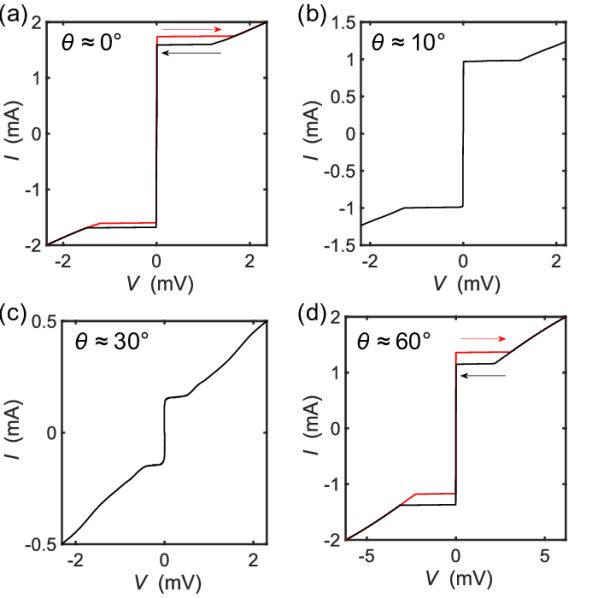
Having observed strikingly different characteristics in NbSe2-NbSe2 junctions prepared using the same fabrication method, we turn our attention to the role of twist angle in these devices. Using the method presented in Fig 1a, we are able to fabricate devices with a determined misalignment angle respective to the crystallographic axes of the two flakes. The results are shown in Fig 3a-d in which we present the current-voltage (-) characteristics of four NbSe2-NbSe2 junctions with twist angles in the range 0 - 60∘. First we examine the 0∘ device, in which hysteresis is observed in the I-V characteristics, indicating the junction is an underdamped Josephson junction. In samples with larger twist angles (10∘, Fig 3b), this hysteresis disappears, giving rise to reversible junctions which show features of quasiparticle gap structure at angles 20∘ (Fig 3c). As the twist angle is increased beyond about 40∘, the gap features disappear and the hysteresis eventually returns near 60∘ (Fig 3d).
Angle resolved photo-emission spectroscopy (ARPES) data27 and density functional theory calculations28 show that there are five electronic bands crossing the Fermi energy in NbSe2. Of these, one is a small Se- -derived "pancake"-shaped hole pocket, while the other four are Nb--derived bands with roughly cylindrical Fermi surfaces centered at the and points in the Fermi surface. Based on ARPES measurements, the Se pancake has been shown to exhibit no superconducting gap, while the Nb-derived sheets display superconductivity which is strongly anisotropic in .29, 30 This anisotropy of the superconducting order parameter is characterised by maxima in the gap at 60∘ intervals around the Fermi sheets. From this, we hypothesise that at twist angles close to 30∘, tunnelling is dominated by processes that couple regions of the Fermi surface with maximum gap in one layer with regions of minimum gap in the other layer. This angular-dependent selectivity in the tunnelling process suppresses the critical current , leading to a lower value of , and non-hysteretic - characteristics.
The observed twist dependence could also be related to the specific atomic arrangement at the interface which depends on the flake terminations as well as any effects arising from relative lateral displacements of the two flakes. However, the latter are expected to be negligible in our large overlap regions, which are many hundreds of unit cells wide. We note that we have minimised any variation in the interface quality and homogeneity by performing all fabrication in the inert environment provided by a nitrogen glovebox.
0.0.3 SQUID performance
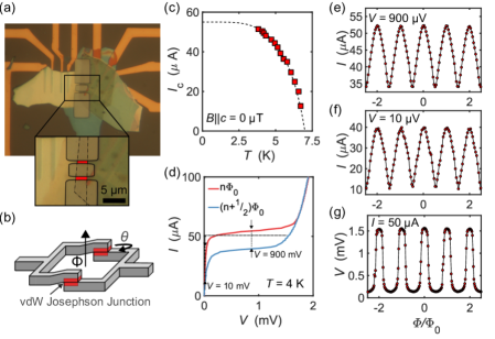
Having established the ability to fabricate high quality non-hysteretic Josephson junctions, we examine the ability to use them in more complex superconducting devices such as superconducting quantum interference devices (SQUIDs). Junction devices were patterned into a SQUID geometry using reactive ion etching as described in Methods. An image of a typical device is shown in Fig 4a, and consists of a superconducting loop between two 600 nm wide Josephson junctions formed in the overlap region of the two NbSe2 flakes. The SQUID loop is of width, 3.5 m, and length, 7.0 m, creating an internal hole of area 24.5 m2. When an external magnetic field is applied, phase shifts are induced between the two junctions leading to interference and a net critical current that oscillates with a period . In practice all real SQUIDs have a finite self-inductance that gives rise to screening currents that can often result in undesirably low values of current modulation ().
To investigate this in our NbSe2-NbSe2 SQUIDs, we used electrical transport measurements to characterise them at temperatures down to = 3.75 K. Figure 4c shows the temperature dependence of the critical current. We observe no reduction of the critical temperature, indicating that etching caused no deterioration in the junction quality. Fig 4d shows the current-voltage characteristics for a NbSe2 SQUID, with the two curves corresponding to the maximum, , and minimum, , measured values of the critical current within a single oscillation period. The modulation of the critical current, () for two different voltage set points, is shown in Fig 4e,f where is the applied magnetic flux. Under a bias voltage of = 900 V the current modulation depth is 33, which increases to 75 for a bias of = 10 V. The noise level of the signal increased slightly at = 10 V due to small temperature oscillations arising from the refrigeration cycle of the closed-cycle cryostat. The inductance parameter characterises the amplitude of the current modulation and is given by , where is the superconducting flux quantum and is the inductance of the SQUID loop. Fitting our measured data to numerical models we estimate that 2, and 10 pH, which is consistent with other estimates of the self-inductance based on the SQUID geometry. The size of the SQUID loop = 24.5 m2 leads to a theoretical value of / 84 , which is close to the measured value of = 78 . Additionally, no decrease in the overall current modulation, , was observed up to 20 mT, the maximum output of the electromagnetic coil.
An important property of modern SQUIDs is the realisation of non-hysteretic - characteristics ( 1), allowing the use of flux-locked loop feedback schemes to dramatically increase the flux resolution.31, 32 We are able to tune this desirable property in our NbSe2 SQUIDS by deterministically controlling the twist angle during device fabrication, with a wide range of angles over which is found to be sufficiently small. Figure 4g shows the voltage under a bias current of 50 A, as a function of magnetic field applied to the SQUID, revealing large voltage modulations with a depth of 1.4 mV. The voltage modulation depth is characterised by , where is the critical current modulation depth, and R is the differential resistance of the SQUID calculated here to be R 28 . A large value of is required to achieve low flux noise SQUID devices as it minimises the noise contribution from the input amplifier to the white flux noise, given by , in flux-locked operation.33 No degradation in or of these SQUIDs was observed after multiple cooling cycles or when remeasured after storage in a nitrogen glovebox for 4 weeks, indicating that they are both stable and suitable for repeated long term use.
0.1 Discussion
In conclusion, we have developed a method to fabricate Josephson junctions and SQUIDs based on a twisted van der Waal heterostructure architecture. The formation of Josephson junctions is achieved using a dry transfer method and requires no ’wet’ lithographic steps. The result is a junction device whose - characteristics can be deterministically tuned via the twist angle. A single lithographic process is then implemented to shape the Josephson junction into a SQUID geometry with typical loop areas of 25 and weak links 600 nm wide. We obtain voltage modulation depths of V 1.4 mV and current modulation depths of I 75 from devices which display long term stability.
Our method demonstrates the ability to fully integrate 2D materials into the design of a high-performance SQUID, paving the way for designer superconducting circuits through incorporation of other 2D materials, each with distinct electronic properties. The utilisation of van der Waals bonded circuits may also have other advantages: here the devices are only anchored to the substrate by the weak vdW force, allowing the possible pick-up and transfer of characterised SQUIDs onto other substrates or materials, while the intrinsically thin nature of 2D materials may allow their incorporation into flexible electronic circuits.34 Other applications for the technology is in the design of superconducting qubits such as those based on flux qubit architectures.35, 36 It is well known that the performance of these is often limited by dissipation, decoherence and noise from two-level defect systems. The single crystalline structure of 2D flakes, along with low defect densities, may provide circuit components with superior performance.
0.2 Method.
Thin flakes of NbSe2 were mechanically exfoliated from high quality single crystals onto silicone elastomer polydimethylsiloxane (PDMS) stamps. Flakes of suitable geometry and thickness were then sequentially transferred onto Si/SiO2 (300 nm oxide) substrates with pre-patterned Au contacts. To ensure crystallographic alignment of the twisted vdW junctions, one single exfoliation of the bulk single crystal is performed which results in multiple thin flakes with aligned crystallographic axes. From this, two neighbouring flakes were chosen with a rotation of the substrate performed after stamping the first flake. The resulting device is thus a twisted vdW junction with the two flakes misaligned by a chosen angle with 1∘ accuracy. The entire dry transfer set-up is housed in a nitrogen glovebox with an oxygen and moisture content <1 ppm, ensuring an oxide free interface. Devices selected for fabrication into SQUIDs were subsequently capped with a thin layer (20 nm) of hexagonal boron nitride (h-BN) using the same dry transfer technique. Following this, a polymethyl methacrylate e-beam resist was spin coated onto the substrate, which was then kept under vacuum (10-6 mbar) overnight to remove any solvent. Next, standard e-beam lithography (EBL) was used to define the area of the junction to be etched to form the SQUID loop, before transfer into an inductively coupled plasma etcher. The sample was then reactively ion etched using an O2 + SF6 mixture, after which the sample was immersed in acetone to remove leftover resist before storage in a nitrogen glovebox.
0.3 Associated Content
0.3.1 Supporting Information
The Supporting Information is available at xxx.
0.4 Author Information
0.4.1 Corresponding Author
*E-mail: L.S.Farrar@bath.ac.uk
0.4.2 Present Address
†Department of Physics, University of Bath, Bath BA2 7AY, United Kingdom
0.4.3 Acknowledgements
The authors thank Peter Heard at the IAC, University of Bristol, for their useful discussions and supporting work at the early phases of this study. The research was funded by the Bath/Bristol Centre for Doctoral Training in Condensed Matter Physics, under the EPSRC (UK) Grant No. EP/L015544. The work at the University of Warwick is supported through EPSRC Grant EP/T005963/1. A.N, Z.J.L, and S.D acknowledge financial support from the Royal Society.
0.4.4 Author contributions
L.F fabricated the devices under the supervision of S.B, with support from A.N. and Z.J.L under the supervision of S.D. G.B grew the single crystals. L.F performed the measurements. L.F and S.B wrote the paper with comments and discussion from all authors.
References
- 1 Fagaly, R.L. Superconducting quantum interference device instruments and applications. Rev. Sci. Instrum. 2006, 77, 101101.
- 2 Likharev, K.K. Superconducting weak links. Rev. Mod. Phys. 1979, 51, 101-159.
- 3 Gurvitch, M.; Washington, M.A.; Huggins, H.A. High quality refractory Josephson tunnel junctions utilizing thin aluminum layers. Appl. Phys. Lett. 1983, 42, 472-474.
- 4 Zeng, L.J.; Nik, S.; Greibe, T.; Krantz, P.; Wilson, C.M.; Delsing, P.; Olsson, E. Direct observation of the thickness distribution of ultra thin AlOx barriers in Al/AlOx/Al Josephson junctions. J. Phys. D Appl. Phys. 2015, 48, 395308.
- 5 Pop, I.M.; Fournier, T.; Crozes, T.; Lecocq, F.; Matei, I.; Pannetier, B.; Buisson, O.; Guichard, W. Fabrication of stable and reproducible submicron tunnel junctions. J. Vac. Sci. Technol. 2012, 30, 010607.
- 6 Kjaergaard, M.; Schwartz, M.E.; Braumüller, J.; Krantz, P.; Wang, J.I.J.; Gustavsson, S.; Oliver, W.D. Superconducting qubits: Current state of play. Annu. Rev. Condens. Matter Phys. 2020, 11, 369-395.
- 7 Scherer, H.; Camarota, B. Quantum metrology triangle experiments: a status review. Meas. Sci. Technol. 2012, 23, 124010.
- 8 Wang, L.; Meric, I.; Huang, P.Y.; Gao, Q.; Gao, Y.; Tran, H.; Taniguchi, T.; Watanabe, K. One-dimensional electrical contact to a two-dimensional material. Science 2013, 342, 614-617.
- 9 Yu, Y.; Ma, L.; Cai, P.; Zhong, R.; Ye C.; Shen J.; Gu, G.D.; Chen, X.H.; Zhang, Y. High-temperature superconductivity in monolayer Bi2 Sr2 CaCu2 O8+δ. Nature 2019, 575, 156-163.
- 10 Farrar, L.S.; Bristow, M.; Haghighirad, A.A.; McCollam, A.; Bending, S.J.; Coldea, A.I. Suppression of superconductivity and enhanced critical field anisotropy in thin flakes of FeSe. npj Quantum Mater. 2020, 5, 1-7.
- 11 Xi, X.; Wang, Z.; Zhao, W.; Park, J.H.; Law, K.T.; Berger, H.; Forró, L.; Shan, J.; Mak, K.F. Ising pairing in superconducting NbSe2 atomic layers. Nat. Phys. 2016, 12, 139-143.
- 12 Castellanos-Gomez, A.; Buscema, M.; Molenaar, R.; Singh, V.; Janssen, L.; Van Der Zant, H.S.; Steele, G.A. Deterministic transfer of two-dimensional materials by all-dry viscoelastic stamping. 2D Mater. 2014, 1, 011002.
- 13 Khestanova, E.; Birkbeck, J.; Zhu, M.; Cao, Y.; Yu, G.L.; Ghazaryan, D.; Yin, J.; Berger, H., Forro, L.; Taniguchi, T.; Watanabe, K. Unusual Suppression of the Superconducting Energy Gap and Critical Temperature in Atomically Thin NbSe2. Nano Lett. 2018, 18, 2623-2629.
- 14 Dvir, T.; Massee, F.; Attias, L.; Khodas, M.; Aprili, M.; Quay, C.H.; Steinberg, H. Spectroscopy of bulk and few-layer superconducting NbSe2 with van der Waals tunnel junctions. Nat. Commun. 2018, 9, 1-6.
- 15 Kim, M.; Park, G.H.; Lee, J.; Lee, J.H.; Park, J.; Lee, H.; Lee, G.H.; Lee, H.J. Strong proximity Josephson coupling in vertically stacked NbSe2–graphene–NbSe2 van der Waals junctions. Nano Lett. 2017, 10, 6125-6130.
- 16 Yabuki, N.; Moriya, R.; Arai, M.; Sata, Y.; Morikawa, S.; Masubuchi, S.; Machida, T. Supercurrent in van der Waals Josephson junction. Nat. Commun. 2016, 7, 1-5.
- 17 Liu, X; Hersam, M.C. 2D materials for quantum information science. Nat. Rev. Mater. 2019, 10, 669-684.
- 18 Ohta, T.; Robinson, J.T.; Feibelman, P.J.; Bostwick, A.; Rotenberg, E.; Beechem, T.E. Evidence for interlayer coupling and moiré periodic potentials in twisted bilayer graphene. Phys. Rev. Lett. 2012, 109, 186807.
- 19 Thompson, J.J.P.; Pei, D.; Peng, H.; Wang, H.; Channa, N.; Peng, H.L.; Barinov, A., Schröter, N.B.M.; Chen, Y.; Mucha-Kruczyński, M. Determination of interatomic coupling between two-dimensional crystals using angle-resolved photoemission spectroscopy. Nat. Commun. 2020, 11, 1-7.
- 20 Pierucci, D.; Henck, H.; Avila, J.; Balan, A.; Naylor, C.H.; Patriarche, G.; Dappe, Y.J.; Silly, M.G.; Sirotti, F.; Johnson, A.C.; Asensio, M.C. Band alignment and minigaps in monolayer MoS2-graphene van der Waals heterostructures. Nano letters. Nano Lett. 2016, 16, 4054-4061.
- 21 Yeh, P.C.; Jin, W.; Zaki, N.; Kunstmann, J.; Chenet, D.; Arefe, G.; Sadowski, J.T.; Dadap, J.I.; Sutter, P.; Hone, J.; Osgood Jr, R.M. Direct measurement of the tunable electronic structure of bilayer MoS2 by interlayer twist.. Nano Lett. 2016, 16, 953-959.
- 22 Dean, C.R.; Wang, L.; Maher, P.; Forsythe, C.; Ghahari, F.; Gao, Y.; Katoch, J. Hofstadter’s butterfly and the fractal quantum Hall effect in moiré superlattices. Nature 2013, 497, 598-602.
- 23 Cao, Y.; Fatemi, V.; Fang, S.; Watanabe, K.; Taniguchi, T.; Kaxiras, E.; Jarillo-Herrero, P. Unconventional superconductivity in magic-angle graphene superlattices. Nature 2018, 556, 43-50.
- 24 Naito, M.; Tanaka, S. Electrical Transport Properties in 2H-NbS2,-NbSe2,-TaS2 and-TaSe2. J. Phys. Soc. Japan 1982, 51, 219-227.
- 25 Likharev, K. K. Dyanmics of Josephson Junctions and Circuits. Gordon and Breach 1986.
- 26 Barone, A.; Paterno, G. Physics and applications of the Josephson effect. Wiley 1982.
- 27 Yokoya, T.; Kiss, T.; Chainani, A.; Shin, S.; Nohara, M.; Takagi, H. Fermi surface sheet-dependent superconductivity in 2H-NbSe2. Science 2001, 294, 2518-2520.
- 28 Johannes, M.D.; Mazin, I.I.; Howells, C.A. Fermi-surface nesting and the origin of the charge-density wave in NbSe2.. Phys. Rev. B 2006, 73, 205102.
- 29 Borisenko, S.V.; Kordyuk, A.A.; Zabolotnyy, V.B.; Inosov, D.S.; Evtushinsky, D.; Büchner, B.; Yaresko, A.N.; Varykhalov, A.; Follath, R.; Eberhardt, W.; Patthey, L. Two energy gaps and Fermi-surface “arcs” in NbSe2. Phys. Rev. Lett. 2009, 102, 166402.
- 30 Rahn, D.J.; Hellmann, S.; Kalläne, M.; Sohrt, C.; Kim, T.K.; Kipp, L.; Rossnagel, K. Gaps and kinks in the electronic structure of the superconductor 2H-NbSe2 from angle-resolved photoemission at 1 K. Phys. Rev. B 2012, 85, 224532.
- 31 Kleiner, R.; Koelle, D.; Ludwig, F.; Clarke, J. Superconducting quantum interference devices: State of the art and applications.. Proc. IEEE 2004, 92, 1534-1548.
- 32 Martínez-Pérez, M.J.; Koelle NanoSQUIDs: Basics recent advances. Phys. Sci. Rev. 2017, 2(8), 1-27.
- 33 Trabaldo, E.; Pfeiffer, C.; Andersson, E.; Arpaia, R.; Kalaboukhov, A.; Winkler, D.; Lombardi, F.; Bauch, T. Grooved Dayem nanobridges as building blocks of high-performance YBa2Cu3O7-δ SQUID magnetometers. Nano Lett. 2009, 19, 1902-1907.
- 34 Kim, S.J.; Choi, K.; Lee, B.; Kim, Y.; Hong, B.H. Materials for flexible, stretchable electronics: graphene and 2D materials. Annu. Rev. Mater. Res. 2015, 45, 63-84.
- 35 Chiorescu, I.; Bertet, P.; Semba, K.; Nakamura, Y.; Harmans, C.J.P.M.; Mooij, J.E. Coherent dynamics of a flux qubit coupled to a harmonic oscillator.. Nature 2004, 431, 159-162.
- 36 Yan, F.; Gustavsson, S.; Kamal, A.; Birenbaum, J.; Sears, A.P.; Hover, D.; Gudmundsen, T.J.; Rosenberg, D.; Samach, G.; Weber, S.; Yoder, J.L. The flux qubit revisited to enhance coherence and reproducibility. Nat. Commun. 2016, 7, 1-9.