Room temperature Mott metal-insulator transition in V2O3 compounds induced via strain-engineering
Abstract
Vanadium sesquioxide (V2O3) is an archetypal Mott insulator in which the atomic positions and electron correlations change as temperature, pressure or doping are varied giving rise to different structural, magnetic or electronic phase transitions. Remarkably, the isostructural Mott transition in Cr-doped V2O3 between paramagnetic metallic and insulating phase observed in bulk has been elusive in thin film compounds so far.
Here, via continuous lattice deformations induced by heteroepitaxy we demonstrate a room temperature Mott metal-insulator transition in 1.5% Cr-doped and pure V2O3 thin films. By means of a controlled epitaxial strain, not only the structure but also the intrinsic electronic and optical properties of the thin films are stabilized at different intermediate states between the metallic and insulating phases, inaccessible in bulk materials. This leads to films with unique features such as a colossal change in room temperature resistivity (R/R up to 100,000 %) and a broad range of optical constant values, as consequence of a strain-modulated bandgap. We propose a new phase diagram for pure and Cr-doped V2O3 thin films with the engineered in-plane lattice constant as a tuneable parameter. Our results demonstrate that controlling phase transitions in correlated systems by epitaxial strain offers a radical new approach to create the next generation of Mott devices.
I Introduction
Vanadium sesquioxide (V2O3) is an example of a Mott insulator presenting both non-isostructural and isostructural metal–insulator transitions (MIT) as a function of temperature, doping and pressure [1, 2, 3] and has attracted great interest for applications. V2O3 undergoes a non-isostructural MIT at 160 K upon cooling from a corundum paramagnetic metallic (PM) phase to a monoclinic antiferromagnetic insulating phase (AFI) [4, 5], yielding a resistivity change of 7 orders of magnitude [1]. In contrast to this low-temperature MIT, the isostructural Mott MIT between paramagnetic metallic (PM) and insulating (PI) phases occurs close to room temperature (RT) and has been observed for a limited range of Cr doping (0.5% – 1.7%) concentration [6]. This transition has been observed in bulk crystals with a resistivity change of 3 orders of magnitude and a variation in a-axis lattice parameter of 1% within the same corundum structure [1, 2].
The bulk phase diagram of V2O3 as a function of temperature, doping and applied pressure has been well established based on extensive experimental data from single crystals [7, 8, 9, 10], and supported by a number of theoretical calculations that successfully predicted the density of states (DOS) of the different phases [11, 12, 13]. In thin films, various deviations from the bulk phase diagram have been observed. For example, recently it has been shown that the AFI phase in thin films is characterized by stripe domains related to different lattice distortions [14]. Then, the low-temperature PM-AFI transition has been reported by many groups [6], while the isostructural RT Mott transition involving PM-PI phases - despite greater interest for applications - has been missing in most studies [6, 15, 16]. This suppression of the RT MIT has been attributed to the clamping effect of the substrate in epitaxial films [16] or to structural disorder and small grain size present in polycrystalline films [6, 15]. Especially, epitaxial strain has so far shown its strong effect on the phase transitions in the vanadate family, which can range from a change in transition temperature [17] or direction dependent electrical properties [18] in VO2 films to a complete suppression of the low-temperature phase transition [19] in V2O3 films.
Salev et al. [20] demonstrated that the low-temperature MIT can actively be modulated through a voltage-actuated PMN-PT [Pb(Mg,Nb)O3-PbTiO3] ferroelectric actuator, which transfers switchable ferroelastic strain into the epitaxial V2O3 film and leads to a giant nonvolatile resistive switching of R/R ~ 1,000%, while the effect at room temperature is only R/R ~ 18%. Querr et al. [21] observed non-volatile resistive switching in Cr-doped V2O3 films, where conducting filaments form as a result of a local electric field driven low-temperature Mott transition. These recent achievements have pointed out the great potential of Mott insulator thin films with large resistivity changes across phase transitions for application in sensors and memory devices. However, triggering the metal-insulator phase transition at room temperature would be even more desirable for their implementation in devices.
The RT MIT has been observed in polycrystalline thin films of Cr-doped V2O3 by optical transmission measurements while electrical resistivity didn’t show a transition [6]. Epitaxial V2O3 thin films showed a local, pressure-induced, transition at RT by means of a contact AFM tip [22] whereas a systematic study by varying the oxygen doping concentration in epitaxial films didn’t show the RT MIT [23]. These results indicate that the RT MIT can be stabilized within a narrow window of conditions, which need to be systematically explored. So far, a generalized phase diagram for V2O3 thin films does not exist but would be highly desirable to gain fundamental understanding about the interplay between epitaxial strain and Mott transition and to use these films in practical applications.
Here, we present a systematic strain-engineering study of 1.5% Cr-doped and pure V2O3 thin films. Our approach is based on the use of precisely engineered oxide heterostructures as artificial substrates to systematically tune the in-plane lattice parameter in the pure and 1.5% Cr-doped V2O3 thin films within and beyond the reported structural states in the bulk. The in-plane lattice parameters of the engineered substrates were gradually adjusted between 4.943 Å and 5.037 Å by varying the precise composition of the thin film buffer layer. Detailed chemical analysis by means of Energy Dispersive X-ray spectroscopy (EDX) confirmed the chemical composition of the buffer layers and the V2O3 films. Extensive structural studies including High Resolution X-Ray Diffraction (HRXRD), Reciprocal Space Maps (RSMs) and High Resolution Transmission Electron Microscopy (HRTEM) revealed the in-plane lattice parameters of the heterostructures and the amount of induced stress. Temperature-dependent electrical resistivity curves were measured using the Van Der Pauw (VDP) configuration. In addition, optical properties were addressed by Spectroscopic Ellipsometry (SE) to illustrate how physical properties in the V2O3 thin films can be fully controlled by epitaxial strain.
The results show an effective transfer of strain achieved by heteroepitaxy leading to a Mott MIT in a wide range of temperatures around RT in 1.5% Cr-doped and pure V2O3 compounds. We observed a colossal change in room temperature resistivity (RTR) with R/R up to ~ 100,000% as well as a significant change in optical constants associated with the strain-modulated bandgap of these Mott insulators. Based on these results, a novel phase diagram of V2O3 thin films was proposed with the RT in-plane parameter as variable. These results demonstrate that meticulous strain engineering is a powerful tool to tune physical properties of strongly-correlated electron systems and also allows accessing novel states unaccesible in bulk. The stabilization and control of the MIT at RT in 1.5% Cr-doped and pure V2O3 thin films is an important achievement towards implementation of Mott materials in devices.
II Experimental
II.1 Thin film growth
All the thin film layers were deposited on (0001)-Al2O3 substrates by oxygen-assisted molecular beam epitaxy (MBE). The vacuum chamber had a base pressure of 10 −9 Torr and it was equipped with RHEED to confirm the epitaxial growth in situ. The oxide heterostructures consist of a 40 nm Cr2O3 epitaxial layer followed by a 30 nm thick (CrFe)2O3 solid solution (y = 0 corresponds to a 40 nm Cr2O3 only). To guarantee that all V2O3 film compounds have the same chemical interface with the heterostructure, an ultrathin 3 nm Cr2O3 layer was deposited on the (CrFe)2O3 alloys with y > 0. Finally, the 60 nm 1.5% Cr-doped and pure V2O3 films were deposited on the artificial substrates composed by the oxide heterostructures.
II.2 Structural characterization
The structural properties of the samples were characterized by means of high-resolution x-ray diffraction (XRD) with a Panalytical X’pert Pro diffractometer using monochromatic K1 radiation of a Cu anode. Out-of-plane measurements in the /2 configuration were done around the symmetric peak () and 2-axes measurements - reciprocal space maps (RSM) - around the asymmetric peak ( ) were performed to extract in-plane and out-of-plane lattice spacings. Besides, the structural quality and composition were also addressed by transmission electron microscopy (TEM) and Energy dispersive X-ray spectroscopy (EDX), respectively. TEM and EDX analysis were performed using a probe-lens corrected JEOL ARM200F scanning transmission electron microscope operating at 200 kV and equipped with a cold-field emission gun and a Centurio energy dispersive x-ray spectrometer. The TEM samples were prepared by means of a focused ion beam (FIB).
II.3 Electrical and optical characterization
Temperature-dependent resistivity measurements in the Van der Pauw (VDP) configuration were performed in an Oxford Optistat CF2-V cryostat using a Keithley 4200-SCS parameter analyzer. The temperature sweep rate was of 1 K per minute. Finally, spectroscopic ellipsometry (SE) measurements from 70 meV to 0.5 eV in the MIR and from 0.5 eV (NIR) to 6 eV (UV) were performed at SENTECH Instruments GmbH in Berlin with a SENDIRA and a SENresearch 4.0 SER 850 DUV ellipsometers, respectively. The ellipsometer angles and were measured at room temperature using three different angles of incidence (, and ). Independent measurements on the layers in the oxide heterostructures were performed before the 1.5% Cr-doped and pure V2O3 films were deposited and the data were fitted applying the Tauc-Lorentz oscillator model [51]. Then, the measurements were repeated on the stack with the top 1.5% Cr-doped or pure V2O3 films and the data were fitted applying the same optical model used for analyzing the layers in the heterostructure.
III Results and discussion
Systematic straining of 1.5% Cr-doped and pure V2O3 films was achieved by using oxide heterostructures consisting of several epitaxial thin films with corundum structure. The thickness of the 1.5 % Cr-doped and pure V2O3 layers was kept to 60 nm. As there is a large lattice mismatch of > 4% between Al2O3 and Cr-doped and pure V2O3 [16], a 40 nm buffer layer of Cr2O3 was first deposited. As demonstrated previously [24], Cr2O3 buffer layer can grow almost relaxed on Al2O3 and enables the subsequent growth of V2O3 structurally decoupled from the substrate with a lattice mismatch of about 0.1%.
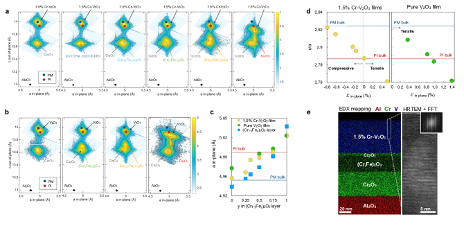
In addition, Cr2O3 has the additional advantage that it can be alloyed with Fe. (CrFe)2O3 also forms a corundum structure with the in-plane lattice parameter that can be changed by more than 1% (between a = 4.959 Å and a = 5.035 Å) [25] by varying the Fe content y. On top of this (CrFe)2O3 layer, an ultrathin Cr2O3 layer (3 nm) was deposited that remained coherent/pseudomorphic with the underlying (CrFe)2O3 layer. This ultrathin Cr2O3 layer ensured that the 1.5% Cr-doped and pure V2O3 films deposited on the buffer stack experienced exactly the same chemical interface so that possible chemical effects of the underlying layer can be excluded. Figure 1e shows a cross-section EDX map obtained from a 1.5% Cr-doped V2O3 film grown on the buffer stack described above. The color code linked to different Cr concentration in the layers reflects the layout of the final heterostructure used for this study. The Cr doping of 1.5% was specifically chosen to ensure the presence of a single PI phase at RT while in pure V2O3 a single PM phase is expected [1, 2]. This allows us to address the effect of strain engineering on both phases involved in the Mott transition.
The in-plane and out-of-plane lattice parameters of the strained (doped and undoped) V2O3 films were determined by means of extensive HRXRD analysis. Figures 1a and b show the RSMs of the 1.5% Cr-doped and pure V2O3 films, measured around the ( ) peak of each layer in the stacks. They clearly demonstrate that all layers in the stacks are single-phase, epitaxial and preserve the corundum structure. No secondary phases were detected. The excellent structural quality is evidenced by the presence of finite-size oscillations in out-of-plane /2 XRD measurements (see Fig. S1 in the supplementary information).
The ( ) peak positions of the Cr2O3/(CrFe)2O3/Cr2O3 stack - and the lattice parameters (a and c) - confirm that the engineered buffer has an in-plane lattice parameter effectively decoupled from the substrate. The blue and red dots in the RSMs in Fig. 1a and b mark the bulk lattice parameters of the PM and PI phases, respectively. By increasing the Fe content in the (CrFe)2O3, the lattice parameters a and c of the 1.5% Cr-doped and pure V2O3 films gradually move from the blue dot position (corresponding PM with aPM, cPM) to the red dot position (corresponding PI with aPI, cPI). For the Fe concentration of (Fe2O3), the lattice parameters go even beyond the PI bulk value.
In-plane lattice parameters of the films are calculated based on the RSM data and summarised in Fig. 1c as a function of the Fe content together with the corresponding values for the buffer layers. The data show that the 1.5% Cr-doped and pure V2O3 films roughly follow the in-plane lattice parameter evolution of the buffer layers. It is important to note that no systematic widening of the RSM peaks is observed as the Fe content changes (except for the cases with ) in the buffer layers. Moreover, by using the Scherrer equation for the out-of-plane diffraction peaks we found that the crystalline coherence is almost the same as the thickness extracted from x-ray reflectivity measurements (only an average difference of 3%) evidencing a good uniformity of the films lattice structure. These results indicate that the designed buffer layers are sufficient to grow films with a well-defined lattice constant across the whole film. In the case of the observed RSM peak broadening could be due to local inhomogeneities or oxygen vacancies that can be more favorable due to the larger tensile strain in these films.
The in-plane lattice parameter of the (CrFe)2O3 layer (light-blue squares) increases linearly with y (only the data point for deviates from this linear trend), evidencing that the produced buffer effectively tailors the amount of induced strain as a function of Fe content. From the in-plane lattice parameters, the resulting in-plane strain was calculated as in-plane= (afilm - abulk)/abulk, with abulk equal to aPI (aPM) for 1.5% Cr-doped (pure) V2O3 films. Figure 1d shows the evolution of the c/a ratio as a function of the strain in the Cr-doped (left) and pure (right) V2O3 films. The continuous decrease of c/a between the PM and PI bulk values (marked by blue and red line, respectively) with in-plane indicates that the c-axis adjusts to the imposed in-plane deformations. The measured changes in the c/a ratio of our strained films slightly deviate from what is expected considering only an elastic deformation: The Poisson ratio for the PI phase in 1.5% Cr-V2O3 for in-plane = -0.8 yiels c/a = 2.831 [26] while we find c/a = 2.822 experimentally. The most remarkable result is the continuous change in c/a between the PM and PI phases, in contrast to the discontinuous one observed in single crystals [2]. This deviation indicates that the bulk and thin films of doped and pure V2O3 behave differently allowing us to explore states with intermediate lattice parameters that are not stable in bulk samples. As highlighted in Fig. 1d, in pure V2O3 films only tensile strain is possible because the Cr2O3 layer has nearly the same in-plane lattice parameter as the PM phase, and alloying with Fe leads to larger in-plane parameters. On the contrary, both compressive and tensile strains are accessible for the 1.5% Cr-doped V2O3 films, which should be in the PI phase in the unstrained bulk phase.
Figure 1e shows a representative color-coded EDX map of the entire stack illustrating the sharp interfaces present across the different layers in the oxide heterostructure. Comparable results were obtained for 1.5% Cr-doped (pure) V2O3 films on the different buffers. In particular, systematic EDX line-scans across the interface between the ultrathin 3 nm Cr2O3 layer and the 1.5% Cr-doped and pure V2O3 layers confirmed that there is no Cr diffusion into the top vanadium oxide layer. The Cr content in the Cr-doped films was estimated to be 1.5% ± 0.3%. Also the HRTEM image and corresponding Fast Fourier Transform (FFT) (shown in the inset) demonstrate the single-crystalline character of the top layer across its whole thickness. The lattice spacings determined by HRTEM were in agreement with those extracted from HRXRD (Fig. 1c).
The temperature-dependent electrical resistivity curves R(T) of the 1.5% Cr-doped and pure V2O3 films are shown in Fig. 2a and b, respectively, along with the reference curves (grey dashed lines) originating from 1% Cr-doped and pure V2O3 single crystals [27]. Note that the (CrFe)2O3 layers are insulating in agreement with the band gaps of 2.1 eV and 3.2 eV for (Fe2O3) and (Cr2O3) [28], respectively, therefore the transport measurements solely probe the V2O3 thin films.
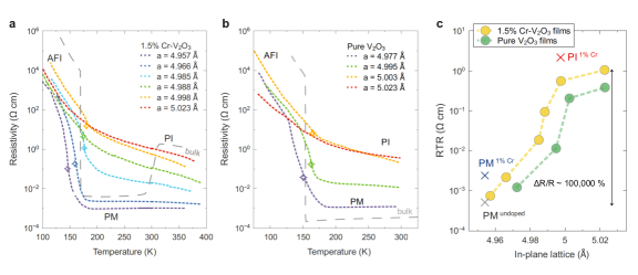
The low temperature (LT) transition can be seen in all samples, except in those with the largest in-plane lattice parameter (dotted red curves in each figure), which correspond to the highest Fe content in the (CrFe)2O3 buffer. The TMIT (marked with star symbols in Fig. 2a and b) was determined from the inflection point in the dLnR(T)/dT curve and increased from 150 K to 180 K with the in-plane lattice parameter in both series. This is similar to the change in TMIT upon Cr doping in bulk (see for example the change in TMIT in the bulk 1.5% Cr-doped and pure V2O3 samples shown in Figs. 2a and b). Nevertheless, there are differences between the strained films - at constant doping - and bulk samples as a function of doping, such as the lack of sharp transitions and significantly reduced resistance jumps at the transition temperature. These differences can be due to several reasons including the in-plane clamping of the film lattice parameters that hampers the structural phase transitions as well as small variations in composition such as Cr-doping and oxygen content. It has been previously reported that increase of tensile strain [29] or oxygen deficiency [30] can cause an increase of RTR and a decrease of resistance ratio across the MIT. Therefore, possible formation of oxygen vacancies could explain the crossing of the R(T) curve for the most strained films (red dotted curves) with the one of films with smaller lattice parameter (yellow dotted curves).
The PM-PI transition close to RT is, as expected, completely absent in the 1.5% Cr-doped V2O3 films for all in-plane parameters, most probably due to the clamping effect [16]. Nonetheless, a significant change of the RTR occurs when changing the in-plane lattice parameter of the films. This trend is also observed in the pure V2O3 thin film series (Fig. 2b). Figure 2c highlights the RTR values as a function of the in-plane lattice parameter for both film series, which clearly shows a PM to PI transition triggered by epitaxial strain. The most striking result is that an in-plane lattice deformation of ~ 1% can trigger a R/R as large as 100,000 % in both the strained 1.5% Cr-doped (yellow circles) and the pure (green circles) V2O3 films. To our knowledge this is the largest change in RTR achieved by epitaxial strain in V2O3 compounds [20, 22, 32].
The RTR of the 1.5% Cr-doped V2O3 film with the smallest in-plane lattice parameter (a = 4.957 Å) is closer to the bulk RTR value of the PM phase of pure V2O3 (marked by the grey cross PMundoped) than to the one of the PM phase of 1% Cr-doped V2O3 compound (marked by the blue cross PM1% Cr). This low RTR value suggests that the metallic state achieved by strain in 1.5% Cr-doped V2O3 thin films is mostly determined by a collective modification of the crystal lattice and electronic band structure in contrast to bulk samples, where the non-perfectly homogeneous distribution of Cr dopants can lead to electron scattering and to higher RTR.
Optical studies have been invaluable for understanding the underlying physics in V2O3 systems [7, 34, 35, 36, 37, 38] because electron correlation effects appear as distinct signatures in the optical conductivity spectra of metallic and insulating phases and the Mott MIT is accompanied by large spectral weight changes [33, 39]. The optical conductivity spectra are shown in Fig. 3a for the strained 1.5% Cr-doped (top) and pure (bottom) V2O3 films. The features (labelled from i to iv) are assigned to the optical transitions depicted in Fig. 3b. The scheme in Fig. 3b shows the density of states (DOS) of metallic (PM) and insulating (PI) phases based on the one-band Hubbard model [33], in which the vanadium 3d band is composed of the quasiparticle peak (QP) around the Fermi level (in the PM phase, defining feature i) and the incoherent bands (so–called Low Hubbard Band (LHB) and Upper Hubbard Band (UHB)) emerging at E - EF = ± U/2, each of width W and separated by the Coulomb energy U. Note that the energy scale of the optical transitions (ii) and (iii) are in the order of U/2 and U, respectively, and the Mott gap in the insulating state is in the order of * = U - W.
Although in the case of V2O3 the realistic multi-orbital scenario of the V 3d bands (i.e., Hubbard bands and QP are composed of two different orbitals) makes the DOS and optical transitions much more complex [36, 40], the optical responses across the Mott MIT can be explained semiquantitatively based on the one-band Hubbard model for the optical conductivity [33]. The real part of the optical conductivity 1, defined as 1() = 20nk, with the angular frequency and 0 the vacuum permittivity [41], has been calculated from the optical constants (index of refraction, n and extinction coefficient, k) derived by Spectroscopic Ellipsometry (SE) experiments performed at RT in an energy range from 0.5 eV to 6 eV (see supplementary information for details).
Consistent with the one-band Hubbard model [33], a signature of the Drude conductivity (feature i, associated with optical transitions within the quasiparticle (QP) peak in the PM phase) is spotted at low energies in both film series with the smallest in-plane lattice parameters. The effects of electron correlation appear in the visible range as features ii (~ 1.4 eV in film spectra) and iii (~ 2.8 eV in film spectra), associated to optical transitions between the QP peak and the Hubbard bands, and between LHB and UHB, respectively. Finally, the peak around 4 eV (labelled as iv) observed in all films is related to transitions from the oxygen 2p bands.
As can be seen in Fig. 3a, the features below 2 eV (i and ii) in 1 significantly decrease, when moving from the PM to the PI state triggered by epitaxial strain, owing to the spectral weight transferred between the Hubbard bands and the QP. The drastic decrease in 1 in this low energy range for the insulating films is directly related to the suppression of the QP and suggests the gradual opening of a gap across the Mott MIT in both strained V2O3 thin film series.
The data in Fig. 3a also reveal isosbestic points near 2.1 eV in both series (marked by circles). Such a point is a characteristic feature of Mott transitions [42], which has been observed in V2O3 thin films, single crystals [36, 37] and VO2 films [38, 43] but for temperature-dependent optical conductivity spectra, which intersect at the same 1 and energy values due to redistributions of spectral weight associated with a change from itinerant to localized electrons. Consequently, the presence of an isosbestic point in the RT optical conductivity spectra of both strained film series further suggests that a Mott phase transition can be triggered by continuous lattice deformation induced by heteroepitaxy.
In Fig. 3c the optical conductivity spectra extended down to the mid-infrared (MIR) regime of the 1.5% Cr-doped and pure V2O3 films with the smallest and largest in-plane lattice parameters are shown. For comparison, the optical conductivity curves obtained from single crystals (1.1% Cr-doped V2O3 single crystal in the PM (220 K) and PI (300 K) phases and pure V2O3 single crystal in the AFI (100 K) phase) [7, 34] are added. These bulk data illustrate that there is only a small drop in spectral weight below 1 eV linked to the opening of a band gap of 0.12 - 0.2 eV [44] for the Mott PM-PI transition in bulk. In contrast, the changes in the strained films are spectacular with a significant spectral weight drop and opening of much larger band gap of up to 0.5 eV. There has been no comparable precedent report in the literature. The gradual decrease of 1 for energies below 1 eV as the lattice parameter increases, and the films become more insulating, indicates that the large spectral weight at low energies might not be an intrinsic property of the PI phase. In addition, it is remarkable that the evolution of 1 of the more insulating films resembles that of the reference V2O3 single crystals in the AFI phase, for which a large band gap of 0.6 eV opens [45]. Our optical data (features ii and iii) indicate that U in the films is of the same order as in bulk. Therefore, a bandwidth reduction as a function of a-axis expansion is possibly the origin of the larger gap in the PI phase in films with a > 4.985 Å, as the Mott gap is * = U - W.
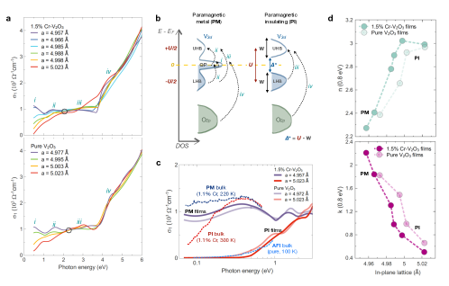
The modulation of the bandgap, associated with intermediate states stabilized across the Mott transition, allows a considerable range of tuning of the optical constants at RT. For example, Fig. 3d displays the optical constants n (top) and k (bottom) at the photon energy of 0.8 eV –which corresponds to a wavelength of 1550 nm typically used in telecommunications– across the Mott transition at RT in both series. At this photon energy, n varies between 2.3 and 3 while k changes between 2.2 and 0.5 as a function of the in-plane lattice parameter. These trends and values are similar to those reported for the temperature driven MIT in VO2 [43, 46], however, the transition in the latter occurs at about 70 ∘C whereas our films show a transition at RT, which is beneficial for device applications. It also has to be noted that the optical constants for V2O3 compounds have not been reported previously. For example, the n and k values of the 1.5% Cr-doped V2O3 films in the whole NIR-UV energy range can be found in Fig. S2.4 of the supplementary information.
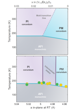
The structural, electrical and optical results reported here for pure and Cr-doped V2O3 thin films indicate that the well-known temperature - doping phase diagram (see Fig. 4(top)) for bulk V2O3 can not be used to represent the different phases achieved via strain engineering. Figure 4(bottom) shows the proposed phase diagram where temperature and in-plane lattice parameter are the variable axes. The absence of a PM-PI phase transition with temperature in pure and 1.5% Cr-doped V2O3 thin films suggests that the 1st order Mott PM-PI transition line (dashed line in Fig. 4(top)) in the bulk phase diagram should be replaced by two straight lines comprising a region of intermediate states between the stable PM and PI ones. These intermediate states are characterized by lattice parameter, RTR and optical constant values between the bulk PM and PI ones. Although these results point to the stabilization of homogeneous intermediate states, local techniques will be necessary to investigate whether there is phase coexistence at nanometric scales.These novel intermediate phases, accessible thanks to the systematic control of strain by heteroepitaxy, can be very interesting for applications based on V2O3 compounds. For example, the changes in resistivity vs lattice parameter could be exploited by inducing lattice deformations when applying an electric field to a nearby piezoelectric material [20] or by depositing the material on a membrane, the effect can be used as a piezoresistive transduction mechanism.
The observation of a PM-PI phase transition by strain engineering in a wide range of temperatures (around room temperature) shows that the Mott transition can be solely driven by lattice deformation. In contrast, the temperature-driven transition to the AFI phase (yellow and green circles in Fig. 4(bottom)) is preserved for the whole range of in-plane lattice parameters studied in this work [47]. Notably, the temperature dependence of the boundary between the PM (or PI) and AFI phases resembles the one for the bulk samples. The robustness of both PM-AFI and PI-AFI transitions against substrate clamping can be related to the considerably larger thermodynamic enthalpy of formation (H = 2.03 kJ/mole and 2.36 kJ/mole, respectively) as compared to the enthalpy of formation for the PM-PI (H = 0.15 kJ/mole) transition [48, 49].
IV Conclusion
In this work, the direct connection between the structure, electronic and optical properties has been exploited to control the Mott MIT phase transition at room temperature in V2O3 thin film compounds. Intermediate states between PM and PI phases, which are not accessible in bulk, are realized by "smart" heteroepitaxy based on fabrication of tailored artificial substrates. It is demonstrated that the Mott MIT can be induced at RT both, in pure and Cr-doped compounds, by strain engineering, leading to films with a colossal R/R 100,000 % and a broad range of optical constants. These results demonstrate that Cr doping is actually not the key control parameter for the RT Mott MIT, in contrast to the observations in the bulk. Moreover, strain engineering leads to a more homogeneous modification of Mott materials compared to chemical doping, where the modification occurs locally on specific sites.
The observed unique electrical and optical properties are attributed to the strain-modulated bandgap beyond the bulk value of 0.1 eV. Our data suggest that the significant spectral weight at low energies in the bulk PI phase, traditionally considered as a hallmark of Mott physics [11, 12, 13, 50], might not be an intrinsic feature but an artefact owing to local inhomogeneities. X-ray absorption and Photo-emission spectroscopy studies together with theoretical calculations considering the lattice deformations and local structures, could give more detailed insight into the changes in the electronic bandstructure and the origin of the modulated bandgap in the strained films.
Finally, the stabilization of a Mott PM-PI transition, in both pure and Cr-doped V2O3 thin films, around room temperature and the possibility to modify the structural, electrical and optical properties in a continuous manner can be used in more practical concepts such as pressure sensors, resonators, acoustic light modulators, and photonic devices in the near-infrared range.
Author contributions
P.H. performed all the MBE thin film growth experiments and the X-ray diffraction measurements and analysis. P.H. and M.M. performed the electrical measurements and analysis. J.W.S did the TEM and EDX analysis. S.P. measured the SE spectra and fitted the data to extract the optical constants. P.H. performed the SE data analysis. J.P.L. conceived the underlying concept and experiments. J.P.L, P.H., M.M. and J. W. S. interpreted the data and wrote the final version. All authors contributed to the writing of the manuscript and the scientific understanding.
Acknowledgments
The authors acknowledge financial support from the EU H2020 Project 688579 PHRESCO and the KU Leuven projects GOA/13/011 Fundamental challenges in Semiconductors and C14/17/080 2D Oxides. We thank Dr. Ruben Lieten for the program to analyze reciprocal space maps data and Dr. Ilse Lenaerts for critically reading the manuscript. P.H. acknowledges support from Becas Chile - CONICYT.
Data availability
The data that support the findings of this study are available from the corresponding authors upon reasonable request.
Supplementary information
The Supporting Information contains X-ray diffraction data of the Cr-doped V2O3 series, an example of the steps followed to fit the Spectroscopic Ellipsometry data and the resulting optical constants of the Cr-doped V2O3 series in the energy range from 0.5 to 6 eV.
References
- [1] McWhan, D. B., Menth, A., Remeika, J. P., Brinkman, W. F. & Rice, T. M. Metal-insulator transitions in pure and doped V2O3. Phys. Rev. B 7, 1920–1931 (1973).
- [2] McWhan, D. B. & Remeika, J. P. Metal-insulator transition in (V1-xCrx)2O3. Phys. Rev. B 2, 3734–3750 (1970).
- [3] McWhan, D. B., Rice, T. M. & Remeika, J. P. Mott transition in Cr-doped V2O3. Phys. Rev. Lett. 23, 1384–1387 (1969).
- [4] Frandsen, B. A. et al. Volume-wise destruction of the antiferromagnetic Mott insulating state through quantum tuning. Nat. Commun. 7, 12519 (2016).
- [5] Dernier, P. D. & Marezio, M. Crystal structure of the low-temperature antiferromagnetic phase of V2O3. Phys. Rev. B 2, 3771 (1970).
- [6] Metcalf, P. A. et al. Electrical, structural, and optical properties of Cr-doped and non-stoichiometric V2O3 thin films. Thin Solid Films 515, 3421–3425 (2007).
- [7] Lupi, S. et al. A microscopic view on the Mott transition in chromium-doped V2O3. Nat. Commun. 1, 105 (2010).
- [8] Mansart, B. et al. Photoemission microscopy study of the two metal-insulator transitions in Cr-doped V2O3. Appl. Phys. Lett. 100, 014108 (2012).
- [9] Rodolakis, F. et al. Inequivalent routes across the Mott transition in V2O3 explored by X-ray absorption. Phys. Rev. Lett. 104, 047401 (2010).
- [10] Rodolakis, F. Evolution of the electronic structure of a Mott system across its phase diagram: X-ray absorption spectroscopy study of (V1-xCrx)2O3. Phys. Rev. B 84, 245113 (2011).
- [11] Hansmann, P. et al. Mott-Hubbard transition in V2O3 revisited. Physica Status sSolidi (b) 250, 1251–1264 (2013).
- [12] Guo, Y.; Clark, S. J. & Robertson, J. Calculation of metallic and insulating phases of V2O3 by hybrid density functionals. J. Chem. Phys. 140, 054702 (2014).
- [13] Basov, D. N.; Averitt, R. D.; Van Der Marel, D.; Dressel, M.& Haule, K. Electrodynamics of correlated electron materials. Rev. Mod. Phys. 83, 471 (2011).
- [14] Ronchi, A. et al. Early-stage dynamics of metallic droplets embedded in the nanotextured Mott insulating phase of V2O3. Phys. Rev. B 100, 075111 (2019).
- [15] Querré, M. et al. Metal-insulator transitions in (V1-xCrx)2O3 thin films deposited by reactive direct current magnetron co-sputtering. Thin Solid Films 617, 56–62 (2016).
- [16] Homm, P. et al. Collapse of the low temperature insulating state in Cr-doped V2O3 thin films. Appl. Phys. Lett. 107, 111904 (2015).
- [17] Aetukuri, N. B. et al. Control of the metal-insulator transition in vanadium dioxide by modifying orbital occupancy. Nature Physics 9, 661 (2013).
- [18] Liang, W. et al. In-plane orientation-dependent metal-insulator transition in vanadium dioxide induced by sublattice strain engineering. NPJ Quantum Materials 4, 39 (2019).
- [19] Autier-Laurent, S.; Mercey, B.; D., C.; Limelette, P. & Simon, C. Strain-induced pressure effect in pulsed laser deposited thin films of the strongly correlated oxide V2O3. Phys. Rev. B 74, 195109 (2006).
- [20] Salev, P.; del Valle, J.; Kalcheim, Y. & Schuller, I. K. Giant nonvolatile resistive switching in a Mott oxide and ferroelectric hybrid. Proceedings of the National Academy of Sciences 116, 8798–8802 (2019).
- [21] Querré, M. et al. Non-volatile resistive switching in the Mott insulator (V1-xCrx)2O3. Physica B: Condensed Matter 536, 327–330 (2018).
- [22] Alyabyeva, N. et al. Metal-insulator transition in V2O3thin films caused by tip-induced strain. App. Phys. Lett. 113, 241603 (2018).
- [23] Thorsteinsson, E. B.; Shayestehaminzadeh, S. & Arnalds, U. B. Tuning metal-insulator transitions in epitaxial V2O3 thin films. Applied Physics Letters 112, 161902 (2018).
- [24] Dillemans, L. et al. Evidence of the metal-insulator transition in ultrathin unstrained V2O3 thin films. Appl. Phys. Lett. 104, 071902 (2014).
- [25] Mashiko, H.; Oshima, T. &Ohtomo, A. Band-gap narrowing in -(CrxFe1-x)2O3 solid-solution films. Appl. Phys. Lett. 99, 241904 (2011).
- [26] Yang, H.; Sladek, R. J. & Harrison, H. R. Pressure dependence of elastic constants of (V1-xCrx)2O3 at 296 K. Phys. Rev. B 31, 5417 (1985).
- [27] Kuwamoto, H.; Honig, J. M. & Appel, J. Electrical properties of the (V1-xCrx)2O3 system. Phys. Rev. B 22, 2626 (1980).
- [28] Chamberlin, S. E. et al. Optical absorption and spectral photoconductivity in -(Fe1-xCrx)2O3 solid-solution thin films. J. Phys.: Condens. Matter 25, 392002 (2013).
- [29] Dillemans L. et al.., Thin Solid Films 520, 4730 (2012).
- [30] Brockman J. et al.., Appl. Phys. Lett. 98 , 152105 (2011).
- [31] Robinson, W. R. High-temperature crystal chemistry of V2O3 and 1% chromium-doped V2O3. Acta Crystallographica Section B 31, 1153–1160 (1975).
- [32] Sakai, J. et al. Strain-induced resistance change in V2O3 films on piezoelectric ceramic disks. J. App. Phys. 125, 115102 (2019).
- [33] Rozenberg, M. J. et al. Optical conductivity in Mott-Hubbard systems. Phys. Rev. Lett. 75, 105 (1995).
- [34] Lo Vecchio, I. et al. Optical properties of V2O3 in its whole phase diagram. Phys. Rev. B 91, 155133 (2015).
- [35] Barker Jr, A. S.& Remeika, J. P. Optical properties of V2O3 doped with chromium. Solid State Commun. 8, 1521–1524 (1970).
- [36] Stewart, M. K. et al. Insulator-to-metal transition and correlated metallic state of V2O3 investigated by optical spectroscopy. Phys. Rev. B 85, 205113 (2012).
- [37] Baldassarre, L. et al. Quasiparticle evolution and pseudogap formation in V2O3: An infrared spectroscopy study. Phys. Rev. B 77, 113107 (2008).
- [38] Qazilbash, M. M. et al. Mott transition in VO2 revealed by infrared spectroscopy and nano-imaging. Science 318, 1750–1753 (2007).
- [39] Brahlek, M. et al. Opportunities in vanadium-based strongly correlated electron systems. MRS Commun. 7, 27–52 (2017).
- [40] Tomczak, J. M. & Biermann, S. Multi-orbital effects in optical properties of vanadium sesquioxide. Journal of Physics: Condensed Matter 21, 064209 (2009).
- [41] Fox, M. Optical properties of solids; Oxford Univ. Press, 2001
- [42] Eckstein, M.; Kollar, M. &Vollhardt, D. Isosbestic points in the spectral function of correlated electrons. J. Low Temp. Phys. 147, 279–293 (2007).
- [43] Li, W. W. et al. Intrinsic evolutions of optical functions, band gap, and higher-energy electronic transitions in VO2 film near the metal-insulator transition region. Appl. Phys. Lett. 99, 241903 (2011).
- [44] Mo, S.-K. et al. Photoemission study of (V1-xMx)2O3 (M = Cr, Ti). Phys. Rev. B 74, 165101 (2006).
- [45] Thomas, G. A. et al. Observation of the gap and kinetic energy in a correlated insulator. Phys. Rev. Lett. 73, 1529 (1994).
- [46] Kana Kana, J. B.; Ndjaka, J. M.; Vignaud, G.; Gibaud, A. & Maaza, M. Thermally tunable optical constants of vanadium dioxide thin films measured by spectroscopic ellipsometry. Opt. Commun. 284, 807–812 (2011).
- [47] The transition temperature for the films with the largest in-plane lattice parameters were obtained from optical transmission measurements.
- [48] Keer, H. V.; Dickerson, D. L.; Kuwamoto, H.; Barros, H. L. C. & Honig, J. M. Heat capacity of pure and doped V2O3 single crystals. J. Solid State Chem. 19, 95–102 (1976).
- [49] Keer, H. V.; Barros, H. L. C.; Dickerson, D. L.; Barfknecht, A. T. & Honig, J. M. Thermal studies on Cr-doped V2O3 crystals. Mater. Res. Bull. 12, 137–143 (1977).
- [50] Kotliar, G. The Mott transition in V2O3 and NiSexS2-x: insights from dynamical mean field theory. Physica B: Condensed Matter 259, 711–714 (1999).
- [51] Jellison Jr, G. E.& Modine, F. A. Parameterization of the optical functions of amorphous materials in the interband region. Appl. Phys. Lett. 69, 371–373 (1996).