Bulk and Edge Properties of Twisted Double-Bilayer Graphene
The emergence of controlled, two-dimensional moiré materials [1, 2, 3, 4, 5, 6] has uncovered a new platform for investigating topological physics [7, 8, 9]. Twisted double bilayer graphene (TDBG) has been predicted to host a topologically non-trivial gapped phase with Chern number equal to two at charge neutrality, when half the flat bands are filled[8, 9]. However, it can be difficult to diagnose topological states using a single measurement because it is ideal to probe the bulk and edge properties at the same time. Here, we report a combination of chemical potential measurements, transport measurements, and theoretical calculations that show that twisted double bilayer graphene can host metallic edge transport while simultaneously being insulating in the bulk. A Landauer-Büttiker analysis of measurements on multi-terminal samples allows us to quantitatively assess edge state scattering. We interpret these results as signatures of the predicted topological phase at charge neutrality.
The tunability of moiré materials [1, 2, 3, 4, 5, 6] by angle and carrier density powers the realization of novel topological phases [7, 8, 9], such as correlated Chern insulators that break time-reversal-symmetry [10, 11, 12, 13, 14, 15, 16]. The long moiré period justifies low-energy effective models that neglect [17] weak scattering between distant regions of momentum space known as valleys. The application of a transverse electric field causes bulk TDBG to open a gap at charge neutrality to a topological state analogous to the quantum spin Hall (QSH) state characterized by a non-zero valley Chern number [8, 9], indicating two pairs of counter-propagating edge states per spin. However, disruption of the moiré pattern on the edge is expected to break the valley symmetry, leaving the states susceptible to scattering and their fate uncertain.
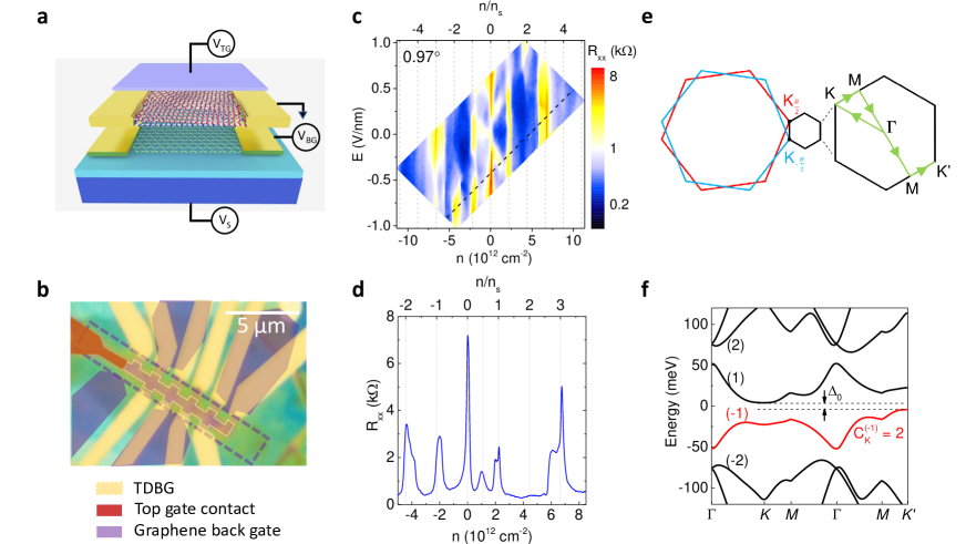
A simultaneous investigation of bulk and edge properties is necessary to reveal the band topology of an electronic system. We employ a sample design shown in Fig. 1a that allows simultaneous electron transport and chemical potential measurements. Our samples consist of a double layer where one layer is a controlled moiré material TDBG, with a twist angle () range of . The second layer is a graphene back-gate (GrBG), consisting of monolayer or bilayer graphene with terminals for resistance measurements. The TDBG and GrBG layers are separated by a hexagonal boron-nitride (hBN) dielectric. The GrBG acts not only as the back-gate, but as a Kelvin probe of the TDBG chemical potential [18, 19]. The double layer is encapsulated in hBN, with an added graphite top-gate, and placed on a SiO2/Si substrate, which serves as an additional gate. This sample architecture allows access to the chemical potential of the TDBG in a wide range of carrier density () and transverse electric field (). Similar double-layers have been used to probe chemical potentials and thermodynamic gaps in bilayer graphene[19], and twisted bilayer graphene[14], albeit without control of the transverse electric field. An optical micrograph of the sample is illustrated in Fig. 1b.
The longitudinal resistance () of the TDBG is measured as a function of top-gate bias () and graphene back-gate bias () to determine the twist angle, and characterize the sample quality. The and values tune and independently according to , and , where is the electron charge, is the vacuum permittivity, and and are the capacitances per unit area of the top- and back-gate, respectively. The values of and can be first determined from the dielectric thickness, and confirmed with magnetotransport measurements (see Supplementary Information section A). Figure 1c shows the contour plot of as a function of and , which exhibits resistance maxima at densities commensurate with cm-2 associated with filling of one moiré band with 4-fold spin-valley degeneracy. Resistance maxima are observed at , consistent with single-particle band structure calculations, as well as correlated insulators at [3, 4, 6, 5]. The maxima at are a surprise because no gap between the second and third moiré bands is predicted in single-particle band calculations. We tentatively attribute the maxima at to a gap opening driven by electron-electron interactions. The twist angle () can be extracted using the equation , where is the graphene lattice constant. Figure 1d shows a line cut of vs. measured along the dashed line in Fig. 1c. Sharp peaks at integer , and fractional further illustrate the observations in Fig. 1c, and highlight the high TDBG sample quality.
We focus primarily on the TDBG properties at charge neutrality where one of the two flat bands, per valley per spin is filled. The bulk topology[20] can be determined from the Bistritzer-MacDonald Hamiltonian[17]. Figure 1e shows how the twisting of the two graphene Brillouin zones forms the moiré Brillouin zone for the valley. In Fig. 1f, we show the calculated band structure at an applied interlayer potential using the parameters in Ref. [20], and highlight the highest valence band at charge neutrality, labelled . This band carries a Chern number , and because all lower bands carry zero Chern number, the total Chern number of the occupied bands is . The valley is related to by time-reversal and must have opposite Chern number. Therefore the phase is characterized by the valley Chern number at charge neutrality.
By tuning the GrBG doping () with a substrate bias (), we are able to directly probe the TDBG chemical potential () as a function of both and . An analysis of the band alignment in the heterostructure (see Supplementary Information section B) shows that when the GrBG is charge neutral (), the TDBG chemical potential satisfies:
| (1) |
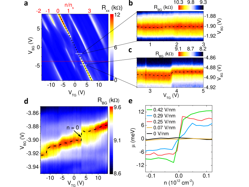
where is the capacitance per unit area between the substrate and the GrBG. To determine the charge neutrality gap at different -fields, we utilize Eq. (1) and Fig. 2a data, which shows a contour plot of vs. and for a TDBG sample with . Along the black dashed diagonal the TDBG density is , while the -field varies. By mapping the longitudinal resistance of the GrBG () vs. and and tracking the GrBG charge neutrality, can be extracted according to Eq. (1). Figure 2b-d show three contour plots of vs. and in the vicinity of , measured at different values. The corresponding and ranges used in Figs. 2b-d are marked by rectangles in Fig. 2a. By changing the value at which the vs. and data are acquired, the -field value at the intersection point of the and lines can be tuned accordingly. Indeed, the TDBG charge neutrality gaps are measured at three values in Figs. 2b-d – (panel b), (panel c), and (panel d). The black dashed lines in Figs. 2b-d illustrate the evolution of GrBG charge neutrality with and , which can be readily converted into a vs. dependence using Eq. (1). The clear step in the GrBG charge neutrality line observed as it crosses the TDBG line shown in Figs. 2c and 2d reveals a thermodynamic gap at the TDBG charge neutrality. In contrast to Figs. 2c and 2d data, in Fig. 2b the line is flat at , indicating the absence of a gap at low -field. Due to our emphasis on TDBG charge neutrality in this work, we show vs. and only in the vicinity of double neutrality in Figs. 2b and 2c. However, the values can also be probed away from . Indeed, Fig. 2d shows a contour plot of vs. and that captures a wider TDBG density range, and displays features that indicate gaps at other moiré filling factors.
Figure 2e summarizes the vs. dependence near , at varied values. The vs. step at marks the opening of a gap () which increases with the applied -field. The evolution of vs. for two samples with twist angles and is shown in Fig. 3a. For comparison Fig. 3a data include the gap at neutrality measured in Bernal stacked bilayer graphene as a function of -field[19]. In both samples the values exceed 100 K at large -fields, and are as high as 300 K in the TDBG.
Figure 3b shows the longitudinal resistivity () vs. measured at for three TDBG samples with values between and . The -field range where opens in the sample is highlighted. The values remain low in the -field range where is negligible, and show a sharp increase concomitant with the gap opening. Surprisingly, the TDBG values then decrease with increasing , and remain well within the expected range of a metallic electron system (, where is Planck’s constant) despite the gap opening for all three samples. We note that similar low values at and at high -fields can be seen in previous studies [21, 22]. Figure 3b also shows vs. at data for a Bernal stacked bilayer graphene [19]. While both the TDBG and Bernal stacked bilayer graphene have a -field dependent gap at neutrality, the vs. dependence of the Bernal stacked graphene is markedly different, quickly reaching large values with increasing , as expected for a prototypical band insulator. In Fig. 3c we show the ratio of the nonlocal resistance () to as a function of and measured in the TDBG. The measurement configuration schematics for and are shown in the Fig. 3c insets. These data show a large ratio at charge neutrality and at high -fields when opens, which signals a distinct change in the current pattern. It is noteworthy that both and values remain well below at charge neutrality, and the ratio remains small elsewhere in Fig. 3c contour plot. The sharp increase in ratio at charge neutrality combined with the low values when opens suggests the presence of edge transport when the TDBG is gapped.
The presence of edge transport may not necessarily stem from non-trivial bulk topology. Indeed, electrostatic edge states due to finite sample width can emerge in small-bandgap semiconductors [23]. To further test the origin of the edge transport in TDBG, it is important to examine a similar twisted system, but with a topologically trivial gap. To this end, in Fig. 3b we include vs. measured at for a TDBG with , i.e. twisted at a small angle with respect to 180∘. Additional data measured in a TDBG with can be found in Supplementary Information section C. The TDBGs with have a similar band structure as TDBGs with , and open a gap at at finite -fields (see Supplementary Information section D). The magnetotransport properties of the TDBG (Fig. S2) reveal a rich Hofstadter butterfly comparable to samples with (Fig. S1), indicating a similarly high quality sample. However, thanks to the C2y symmetry in TDBGs with the gap at neutrality is topologically trivial with [9]. Figure 3d compares vs. at at different temperatures measured in the TDBG (left panel) with vs. at for the three TDBGs twisted with respect to (right panel). The contrast between the two sets of samples is noteworthy – quickly reaches values significantly larger than , with an insulating temperature dependence in the TDBG, while the TDBGs with show lower than when the gap opens at neutrality. The contrast between the TDBG and the TDBGs suggests non-trivial edge transport in the TDBGs with , which we associate with the emergence of a topological valley Chern insulator.
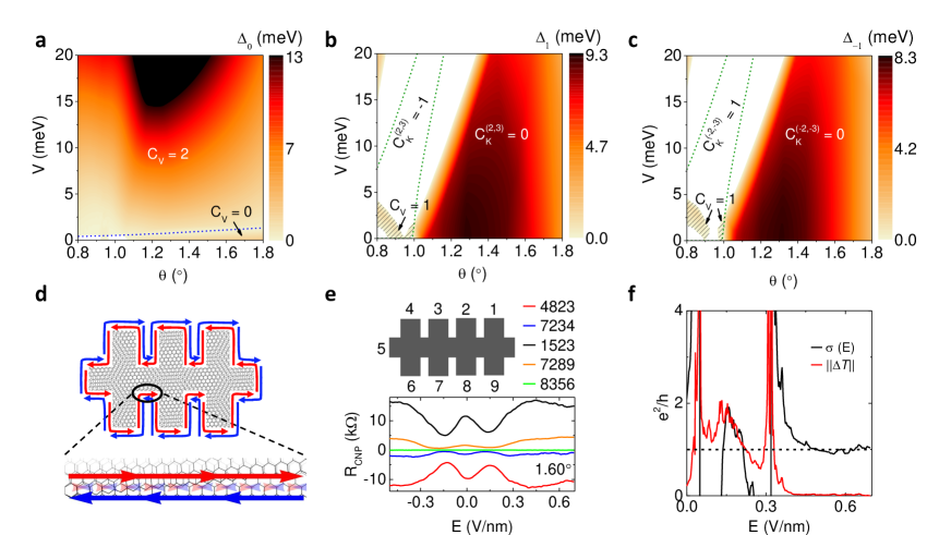
To better describe the TDBG band structure and topology, we compute a single-particle phase diagram for TDBG[20] for and varying , controlled by the applied -field. We extract the indirect gap at charge neutrality from the band structure as depicted in Fig. 1f, and compute the Chern numbers of the occupied bands. Figure 4a shows a contour plot of vs. and , which reveals a gap closing and reopening (blue dashed line) for all angles at small . Beyond the gap closing, corresponding to larger -fields, we find a gapped topological phase with . The results are consistent with the experimental data in our samples. Interestingly, Fig. 4a data predicts a trivial insulator for with a gap of approximately at which may account for the decrease at small -fields for the TDBG in Fig. 3b, and observed for TDBGs with in Ref. [24].
Figures 4b and 4c show the phase diagrams at , dominated by a gapless phase and a trivial insulator. However, at and small -fields, a gapped state with (shaded area) appears for both . In this state at in valley , the upper flat band has Chern number which only partially cancels the Chern number carried by all valence bands. Similarly, at , the dispersive bands below the flat bands carry Chern number , and the lower flat band carrying Chern number is unoccupied. It is noteworthy that in addition to the large observed at , Fig. 3c data shows satellites of finite at , a possible signature of the topological state at this filling factor. There is also a peak at , but with a weaker nonlocal resistance, indicating some degree of particle-hole symmetry breaking. This finding is consistent with the shaded region of Fig. 4c data which is interrupted by a metallic phase near .
To quantitatively probe the edge state transport (Fig. 4d) we employ the Landauer-Büttiker (LB) formalism [25, 26, 27]. The TDBG has nine terminals which enables a variety four-terminal resistance measurements relating the currents and voltages (Fig. 4e). The LB equation, normalized by to include spin degeneracy, reads
| (2) |
Here is the transmission probability from , in our sample. Because the disruption of the moiré pattern on the edge and the sample geometry the transmission matrix is not expected to take a simple form. We derive an exact inverse relating resistance measurements to the entries of , extending prior results for a four-terminal sample[28] (see Supplementary Information section E). Using the matrix we then extract the order parameter
| (3) |
where , the total edge conductance, is equal to when edge states do not back-scatter (see Supplementary Information section E.6). Figure 4f shows vs. and reveals a divergence in the order parameter at the topological phase transition at . For larger in the topological phase, decays quickly to a constant finite value. To further illustrate the edge transport, Fig. 4f shows , the average deviation of from defined by the Frobenius norm (see Supplementary Information section E.6). A small value of means that is close to in every entry. Once the gap is open, we find that , indicating that the whole matrix and the edge states it describes are independent of , suggestive of topological effects.
Lastly, we comment on the contrast with Bernal stacked bilayer graphene, a material with large Berry curvature at the Brillouin zone corners, and theoretically expected to possess edge states for specific terminations [29, 30]. In TDBG, we find the transverse edge state localization length , whereas in Bernal graphene (Supplementary Information section F), making the edge states much more sensitive to edge disorder. This implies that edge states scattering in TDBG is significantly reduced thanks to the long moiré period.
In summary, simultaneous thermodynamic and transport properties can provide unique insights into band topology effects in moiré materials, particularly for states that do not break time-reversal symmetry. The data suggests the emergence of a tunable topological insulator in TDBG, as a consequence of non-zero valley Chern numbers of the moiré bands.
Acknowledgements
We thank Zhi-Da Song and Biao Lian for helpful discussions. The work at The University of Texas was supported by the National Science Foundation Grants MRSEC DMR-1720595, EECS-1610008, EECS-2122476, Army Research Office under Grant No. W911NF-17-1-0312, and the Welch Foundation grant F-2018-20190330. Work was partly done at the Texas Nanofabrication Facility supported by NSF Grant No. NNCI-1542159. B.A.B. was supported by the DOE Grant No. DE-SC0016239, the Schmidt Fund for Innovative Research, Simons Investigator Grant No. 404513, the Packard Foundation, the Gordon and Betty Moore Foundation through Grant No. GBMF8685 towards the Princeton theory program, and a Guggenheim Fellowship from the John Simon Guggenheim Memorial Foundation. Further support was provided by the NSF-EAGER No. DMR 1643312, NSFMRSEC No. DMR-1420541 and DMR-2011750, ONR No. N00014-20-1-2303, BSF Israel US foundation No. 2018226, and the Princeton Global Network Funds. J.H.A. acknowledges support from a Marshall Scholarship funded by the Marshall Aid Commemoration Commission. A.H.M. acknowledges support from Welch Foundation grant F1473. K.W. and T.T. acknowledge support from the Elemental Strategy Initiative conducted by the MEXT, Japan (Grant Number JPMXP0112101001), JSPS KAKENHI (Grant Numbers JP19H05790 and JP20H00354).
References
- [1] Yuan Cao et al. “Correlated Insulator Behaviour at Half-Filling in Magic-Angle Graphene Superlattices” In Nature 556.7699, 2018, pp. 80–84 DOI: 10.1038/nature26154
- [2] Yuan Cao et al. “Unconventional Superconductivity in Magic-Angle Graphene Superlattices” In Nature 556.7699, 2018, pp. 43–50 DOI: 10.1038/nature26160
- [3] G. Burg et al. “Correlated Insulating States in Twisted Double Bilayer Graphene” In Phys. Rev. Lett. 123.19, 2019, pp. 197702 DOI: 10.1103/PhysRevLett.123.197702
- [4] Cheng Shen et al. “Correlated States in Twisted Double Bilayer Graphene” In Nat. Phys. 16.5, 2020, pp. 520–525 DOI: 10.1038/s41567-020-0825-9
- [5] Yuan Cao et al. “Tunable Correlated States and Spin-Polarized Phases in Twisted Bilayer–Bilayer Graphene” In Nature 583.7815, 2020, pp. 215–220 DOI: 10.1038/s41586-020-2260-6
- [6] Xiaomeng Liu et al. “Tunable Spin-Polarized Correlated States in Twisted Double Bilayer Graphene” In Nature 583.7815, 2020, pp. 221–225 DOI: 10.1038/s41586-020-2458-7
- [7] Fengcheng Wu et al. “Topological Insulators in Twisted Transition Metal Dichalcogenide Homobilayers” In Phys. Rev. Lett. 122.8 American Physical Society, 2019, pp. 086402 DOI: 10.1103/PhysRevLett.122.086402
- [8] Narasimha Raju Chebrolu, Bheema Lingam Chittari and Jeil Jung “Flat Bands in Twisted Double Bilayer Graphene” In Phys. Rev. B 99.23, 2019, pp. 235417 DOI: 10.1103/PhysRevB.99.235417
- [9] Mikito Koshino “Band Structure and Topological Properties of Twisted Double Bilayer Graphene” In Phys. Rev. B 99.23, 2019, pp. 235406 DOI: 10.1103/PhysRevB.99.235406
- [10] Aaron L. Sharpe et al. “Emergent Ferromagnetism near Three-Quarters Filling in Twisted Bilayer Graphene” In Science 365.6453 American Association for the Advancement of Science, 2019, pp. 605–608 DOI: 10.1126/science.aaw3780
- [11] M. Serlin et al. “Intrinsic Quantized Anomalous Hall Effect in a Moiré Heterostructure” In Science 367.6480 American Association for the Advancement of Science, 2020, pp. 900–903 DOI: 10.1126/science.aay5533
- [12] Shuang Wu et al. “Chern Insulators, van Hove Singularities and Topological Flat Bands in Magic-Angle Twisted Bilayer Graphene” In Nat. Mater. 20.4 Nature Publishing Group, 2021, pp. 488–494 DOI: 10.1038/s41563-020-00911-2
- [13] Ipsita Das et al. “Symmetry-Broken Chern Insulators and Rashba-like Landau-Level Crossings in Magic-Angle Bilayer Graphene” In Nat. Phys. 17 Nature Publishing Group, 2021, pp. 710–714 DOI: 10.1038/s41567-021-01186-3
- [14] Jeong Min Park et al. “Flavour Hund’s Coupling, Chern Gaps and Charge Diffusivity in Moiré Graphene” In Nature 592.7852 Nature Publishing Group, 2021, pp. 43–48 DOI: 10.1038/s41586-021-03366-w
- [15] Kevin P. Nuckolls et al. “Strongly Correlated Chern Insulators in Magic-Angle Twisted Bilayer Graphene” In Nature 588.7839 Nature Publishing Group, 2020, pp. 610–615 DOI: 10.1038/s41586-020-3028-8
- [16] Youngjoon Choi et al. “Correlation-Driven Topological Phases in Magic-Angle Twisted Bilayer Graphene” In Nature 589.7843 Nature Publishing Group, 2021, pp. 536–541 DOI: 10.1038/s41586-020-03159-7
- [17] Rafi Bistritzer and Allan H. MacDonald “Moiré Bands in Twisted Double-Layer Graphene” In Proc. Natl Acad. Sci. USA 108.30 National Academy of Sciences, 2011, pp. 12233–12237 DOI: 10.1073/pnas.1108174108
- [18] Seyoung Kim et al. “Direct Measurement of the Fermi Energy in Graphene Using a Double-Layer Heterostructure” In Phys. Rev. Lett. 108.11, 2012, pp. 116404 DOI: 10.1103/PhysRevLett.108.116404
- [19] Kayoung Lee et al. “Chemical Potential and Quantum Hall Ferromagnetism in Bilayer Graphene” In Science 345.6192, 2014, pp. 58–61 DOI: 10.1126/science.1251003
- [20] G. Burg et al. “Evidence of Emergent Symmetry and Valley Chern Number in Twisted Double-Bilayer Graphene. Preprint at http://arxiv.org/abs/2006.14000”, 2020 arXiv: http://arxiv.org/abs/2006.14000
- [21] Subhajit Sinha et al. “Bulk Valley Transport and Berry Curvature Spreading at the Edge of Flat Bands” In Nat. Commun. 11.1 Nature Publishing Group, 2020, pp. 5548 DOI: 10.1038/s41467-020-19284-w
- [22] Minhao He et al. “Symmetry Breaking in Twisted Double Bilayer Graphene” In Nat. Phys. 17.1 Nature Publishing Group, 2021, pp. 26–30 DOI: 10.1038/s41567-020-1030-6
- [23] Fabrizio Nichele et al. “Edge Transport in the Trivial Phase of InAs/GaSb” In New J. Phys. 18.8 IOP Publishing, 2016, pp. 083005 DOI: 10.1088/1367-2630/18/8/083005
- [24] Yanbang Chu et al. “Phonons and Quantum Criticality Revealed by Temperature Linear Resistivity in Twisted Double Bilayer Graphene. Preprint at http://arxiv.org/abs/2104.05406”, 2021 arXiv: http://arxiv.org/abs/2104.05406
- [25] M. Büttiker “Four-Terminal Phase-Coherent Conductance” In Phys. Rev. Lett. 57 American Physical Society, 1986, pp. 1761–1764 DOI: 10.1103/PhysRevLett.57.1761
- [26] M. Büttiker “Absence of backscattering in the quantum Hall effect in multiprobe conductors” In Phys. Rev. B 38 American Physical Society, 1988, pp. 9375–9389 DOI: 10.1103/PhysRevB.38.9375
- [27] Markus König et al. “Quantum Spin Hall Insulator State in HgTe Quantum Wells” In Science 318.5851, 2007, pp. 766–770 DOI: 10.1126/science.1148047
- [28] M. Büttiker “Symmetry of electrical conduction” In IBM J. Res. Dev. 32.3, 1988, pp. 317–334 DOI: 10.1147/rd.323.0317
- [29] A.. Rozhkov, A.. Sboychakov, A.. Rakhmanov and Franco Nori “Electronic Properties of Graphene-Based Bilayer Systems” In Phys. Rep. 648, 2016, pp. 1–104 DOI: 10.1016/j.physrep.2016.07.003
- [30] D.. Costa et al. “Energy levels of bilayer graphene quantum dots” In Phys. Rev. B 92 American Physical Society, 2015, pp. 115437 DOI: 10.1103/PhysRevB.92.115437
- [31] Jonah Herzog-Arbeitman, Zhi-Da Song, Nicolas Regnault and B. Bernevig “Hofstadter Topology: Noncrystalline Topological Materials at High Flux” In Phys. Rev. Lett. 125 American Physical Society, 2020, pp. 236804 DOI: 10.1103/PhysRevLett.125.236804
- [32] Christian Brouder et al. “Exponential Localization of Wannier Functions in Insulators” In Phys. Rev. Lett. 98.4 American Physical Society, 2007, pp. 046402 DOI: 10.1103/PhysRevLett.98.046402
- [33] G. Golub and W. Kahan “Calculating the Singular Values and Pseudo-Inverse of a Matrix” In J. Soc. Ind. Appl. Math. Ser. B Numer. Anal. 2.2 Society for Industrial and Applied Mathematics, 1965, pp. 205–224 JSTOR: 2949777
- [34] E. Prada, P. San-Jose, L. Brey and H.. Fertig “Band Topology and the Quantum Spin Hall Effect in Bilayer Graphene” In Solid State Commun. 151.16, 2011, pp. 1075–1083 DOI: 10.1016/j.ssc.2011.05.016
- [35] John R. Schaibley et al. “Valleytronics in 2D materials” In Nat. Rev. Mater. 1.11, 2016, pp. 16055 DOI: 10.1038/natrevmats.2016.55
Methods
Sample Fabrication
All the graphene, graphite, and hBN flakes used to fabricate our samples are mechanically exfoliated, and inspected by optical microscopy. The hBN flakes are subsequently inspected with atomic force microscopy to confirm their thickness and surface roughness. Optical contrast and Raman spectroscopy were used to confirm the layer number for monolayer and bilayer graphene. The TDBG samples are assembled by sequential pick-up steps utilizing a hemispherical polypropylene carbonate (PPC)/polydimethylsiloxane (PDMS) handle. The back-gate structure is first prepared by picking up a monolayer or bilayer graphene with hBN, followed by a set of pre-trimmed graphite contacts. The stacked structure is then placed on a SiO2/Si substrate, or a prepared hBN/graphite stack, in the case of samples with graphite substrate gate, to form the bottom structure of the sample. Starting with another large bilayer graphene flake trimmed into two separate sections by lithography and O2 plasma etching, another hBN is used to sequentially picked up the two sections, with a rotation of a small, controlled angle between the two pick-ups, to form the TDBG. The TDBG is then placed on the bottom structure, and a graphite top-gate is place on the TDBG. The structure is then trimmed into a Hall-bar shaped channel using CHF3 and O2 plasma etching, which also creates exposed one-dimensional edges of the TDBG and the graphite contacts to the back-gate. Metal (Cr/Pd/Au) edge contacts are evaporated to finalize the sample.
Measurement Setup
The samples are measured in a variable-temperature liquid 4He cryostat with a base temperature of 1.5 K. Three- and four-point resistance measurements low-frequency (7 – 13 Hz) lock-in techniques are performed on the TDBG and GrBG layers. Source currents of different frequencies are used on TDBG and GrBG layers, to avoid cross-talk. A radio-frequency transformer is used to flow an AC current in the GrBG layer while applying a DC bias .
Supplementary Information
Appendix A Magnetotransport Measurements and Hofstadter Butterfly
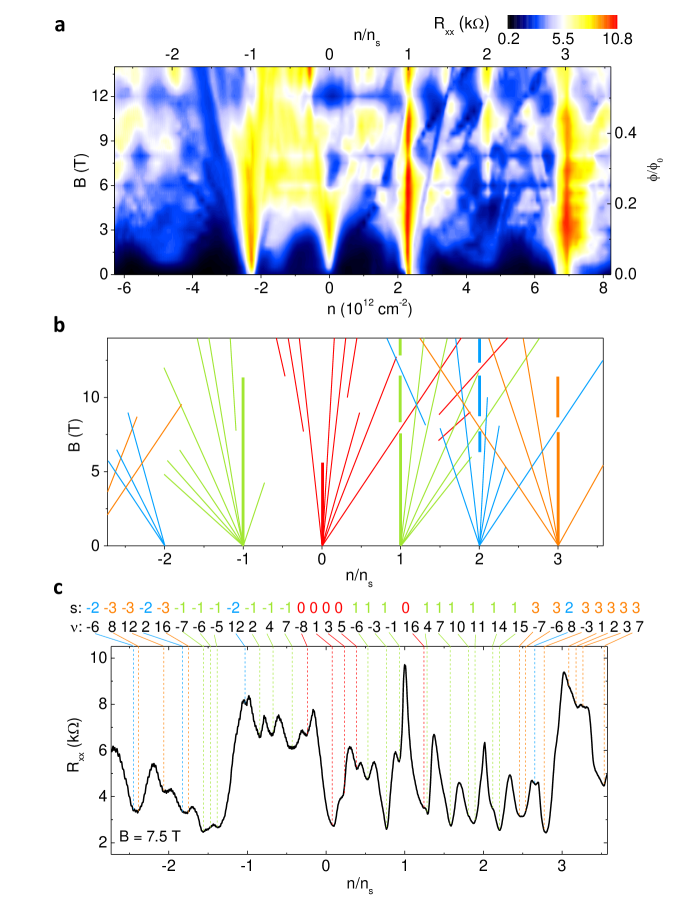
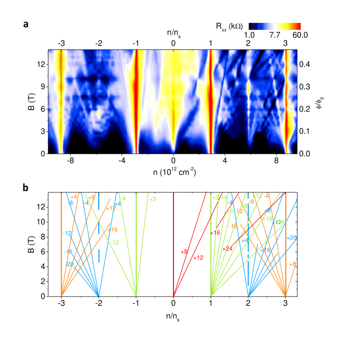
Magnetotransport measurements are performed for the TDBG samples in perpendicular magnetic field up to . In Fig. S1a and Fig. S2a, we show vs. and , with right axis as , measured in the and samples at constant -fields and , respectively. Here, is the magnetic flux per moiré unit cell, , is the moiré unit cell area , and is the magnetic flux quanta . The sample is kept at a fixed -field during the measurement by sweeping the top and back-gate biases simultaneously, while keeping . The ratio is determined by the slope of the charge neutrality line from the contour of vs. and . For both and samples, a fractal Hofstadter butterfly spectrum is observed. The Hofstadter butterfly consists of trajectories of Landau level gaps in energy spectrum developed under a periodic potential and perpendicular magnetic field, and can be characterized by the Diophantine relation
| (4) |
and are integers associated with Landau level and moiré subband fillings, respectively, and index the QHSs. By fitting the fractal Hofstadter butterfly with Eq. 4, we are able to determine the carrier densities at each (, ) point, and confirm the capacitances of the top and bottom gates. In the sample, the capacitances are extracted to be and . We summarize the QHSs observed in Fig. S1a (Fig. S2a) and show them in Fig. S1b (Fig. S2b). The QHS fans originated from , , and are observed. The QSHs with , namely at densities with integer , are marked with vertical lines in Fig. S1b and Fig. S2b. The vertical lines at integer interrupted by QHSs originated from a different -index are marked in Fig. S1b and Fig. S2b, as a signature of nontrivial topology [31].
Figure S1c shows as a function of taken at , which shows oscillations associated with well-developed QHSs. We show the and indices for the resistance minima observed, and note the presence of indices not a multiply of suggests the lifting of spin and valley symmetry. The observation of plethora of the QHSs testifies to the high quality of our samples.
Appendix B Chemical Potential Extraction
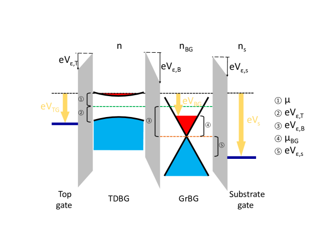
The chemical potentials of TDBG and GrBG can be written in terms of gate biases and capacitances of the heterostructure. We begin by analyzing the band diagram in Fig. S3, where , , and are the changes in electrostatic potential across the top, back, and substrate dielectrics, respectively. is the carrier densities in the substrate gate, and is the chemical potential of the GrBG. An applied is the sum of the potential drop across the top-gate dielectric and the chemical potential of the TDBG:
| (5) |
where is the electron charge. Similarly, and can also be written as:
| (6) |
| (7) |
while the potential drops across the dielectrics can be written as
| (8) |
| (9) |
| (10) |
here, , , and are the gate capacitances of the top, back and substrate gates, respectively. Note that during all the measurements, the potential of the TDBG is always kept at ground. Combining the six equations above, the following relations can be obtained:
| (11) |
| (12) |
At GrBG charge neutrality, and are satisfied, the relations above become:
| (13) |
| (14) |
we then obtain the chemical potential of TDBG in terms of (, , , ) at GrBG charge neutrality,
| (15) |
We note that, according to Eq. 15, the resolution of the chemical potential measurement is limited by the accuracy in determining the back-gate charge neutrality as a function of , .
Appendix C Additional Data
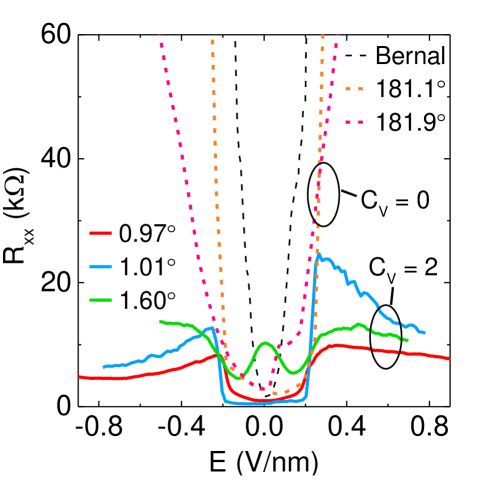
Figure S4 shows charge neutrality resistance () vs. -field data measured in TDBGs with , , , and . The data shows that the charge neutrality resistance in the TDBGs with increases with the -field and reaches values larger than , supporting the findings that the TDBG with a twist angle is a band insulator at charge neutrality at finite -field, in contrast with the TDBG with . For comparison, vs. data for a Bernal stacked bilayer graphene is included.
Appendix D Theoretical Calculation of the Topological Phase Diagram
In this Appendix, we briefly describe the band structure calculations and determination of the phase diagrams, giving the Chern number and gap as a function of and . Our starting point is the Bistritzer-MacDonald Hamiltonian considered in Ref. [20]. To summarize, the TDBG band structure is computed across a moiré Brillouin Zone on the scale of where is the moiré twist angle and is the graphene lattice constant. The Bistritzer-MacDonald Hamiltonian, per spin per valley, is written as a honeycomb continuum model in momentum space by plane-wave expansions which we truncate to five shells of moiré reciprocal lattice vectors. We do not employ the particle-hole symmetric approximation in order to uncover finer details of the phase diagram.
The band gaps shown in Figs. 4a-c are determined by computing the band structure on a fine mesh of angle (from to ), and inter-layer potential (from to ). We note that the conversion between and , depends on a phenomenological screening parameter . Here, is the electron charge and is the inter-layer distance. A quantitative understanding of screening in TDBG is beyond the scope of the study.
As shown in Fig. 1f, the low energy bands are labeled in a convention where valence bands at charge neutrality are indexed with negative numbers, e.g. band is the second band below charge neutrality, and the conduction bands are indexed with a positive number, e.g. band is the upper flat band just above charge neutrality. To compute the Chern number over a single band (or set of bands), we use the formula [32]
| (16) |
where is the projection matrix on the band , i.e. is the eigenvector of band , are the coordinates of the moiré Brillouin zone which has area , approximates the numerical derivative, and is the number of points in hexagonal moiré BZ making up the momentum sum. Eq. (16) is written in terms of projectors and hence is manifestly gauge-invariant. We take to be large so that very good quantization is observed in the calculated Chern numbers. To calculate the Chern number of a connected set of bands, should be understood as a matrix whose columns are the eigenvectors of the bands under consideration, thereby generalizing the one band example. By computing the Chern numbers of the occupied bands at a giving filling, we determine the total Chern number in the valley by
| (17) |
and, by time-reversal symmetry , so finally
| (18) |
We now discuss the phase diagrams obtained in this manner in Figs. 4a-c. At charge neutrality (Fig. 4a) we find that for small there is a gapped region where the system is a trivial insulator with . While the experimental results do not show a gap at , its theoretical value is below the resolution limit of our thermodynamic chemical potential measurements.
A line of gap closings (dashed in blue in Fig. 4a) separates this region from the nontrivial phase of interest in this work where . We note that the bands which carry the nontrivial Chern numbers change within this region, which we show with green dashed lines in Figs. 4b-c. For larger angles, the highest valence band carries , whereas for smaller angles, a band-touching transition within the occupied manifold separates a region where and , so the Chern number is split over the highest three valence bands. At charge neutrality, there is no difference between these phases, but when both () or neither () of the flat bands are filled, this transition changes the observable valley Chern number. Let us first discuss Fig. 4b where the upper flat band is occupied (). The shaded region in this plot highlights a gapped phase where the valley Chern number of the bands below charge neutrality is partially canceled by the Chern number of the upper flat band, leading to . At larger angles where , there is a complete cancellation and . The analogous situation appears for filling shown in Fig. 4c where for small angles and hence . For larger angles, and the occupied band is trivial. However, the shaded region in this case is interrupted by a gap closing due to the small particle-hole symmetry breaking.
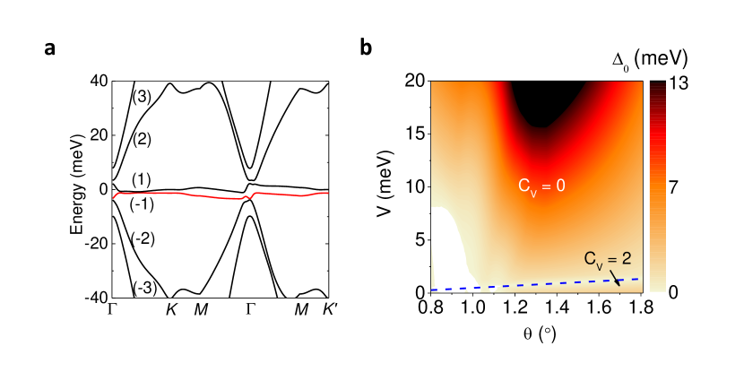
We now discuss the band structure and topology of the TDBG device, which is AB-BA stacked due to the additional rotation. The details of the system can be found in Ref. [8] and Ref. [9], as well as a discussion of the topology. The salient features for this work are (1) the moiré band structure is very similar to small-angle TDBG, featuring two nearly flat bands at charge neutrality and a pair of energetically connected passive bands below and above shown in Fig. S5a, and (2) the topology of the system is very different, providing a strong point of comparison. We show the full phase diagram in Fig. S5b calculated using Eq. 16. The most important property of the system is its behavior in large applied -field at charge neutrality where the system is a trivial insulator with . This is in stark contrast to the phase diagram of TDBG, shown in Fig. 4a, where the system is a nontrivial valley Chern insulator in large field. An experimental comparison of these systems shows different transport behavior, which we associate with the differences in band topology.
Appendix E Landauer-Büttiker Formalism
In this Appendix, we review the Landauer-Büttiker formalism and highlight how the charge conservation and gauge invariance are taken into account. We then present our exact inverse which relates measured resistances to the transmission matrix that quantitatively describes the edge states for an arbitrary number of terminals. We also define the conductance order parameter and discuss its properties. This analysis is general and can be directly applied to nonlocal transport measurements in any system. Finally, we describe the analysis of the nonlocal measurements in our TDBG samples and give quantitative evidence for topologically protected edge states.
E.1 Introduction
We consider a system of electrodes which may be connected to conventional electronic voltage or current leads, as depicted in Fig. S6. In the Landauer-Büttiker (LB) formalism[28, 25, 26], the measured current and voltage are related by the transmission probabilities , where is the probability of transport from , in the form
| (19) |
where is the number of edge states of a given chirality. For the case of a valley Chern insulator with spin degeneracy, we have . In experiments, the current is injected into one terminal and exits through another, so the vector is nonzero and opposite for two entries. Using a voltimeter, differences in the entries of can be measured between any pair of terminals.
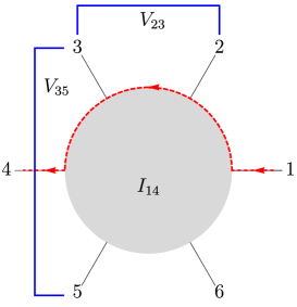
The LB equation Eq. 19 is essentially Ohm’s law on the edge, saying that the current is proportional to the voltage drops weighted by the transmission probabilities. As an example, consider a perfectly clean quantum hall system with , yielding a single chiral edge state. Because the state is chiral, electrons are only transported in one direction around the sample, and they are dissipationless. Hence where are taken mod to be periodic around the sample. In this case, Eq. 19 gives
| (20) |
From Ohm’s law, , we find a resistance of .
E.2 Gauge Invariance and Current Conservation
The LB equation is subject to current conservation and gauge invariance. Current conservation means that the physical currents must satisfy , and gauge invariance means that the LB equation must be invariant under . Current conservation means that physical currents occupy an dimensional subspace of subject to , and gauge invariance gives an equivalence relation . that reduces physically distinct voltage configurations to an dimensional subspace of . Consider Eq. 19 for . which corresponds to every terminal being at the same voltage, so no current flows and . Eq. 19 then reads
| (21) |
so the th row sum is equal to the th column sum. Eq. 21 ensures that and are physically indistinguishable, which is a requirement of gauge invariance. We now show that for the LB equation to be consistent, there is gauge invariance if there is current conservation. We can rewrite the LB equation in matrix notation as
| (22) |
where . Note that the sum of the elements of each row of is equal to zero. Hence, has a nontrivial nullspace which is one-dimensional and is spanned by the vector . This is due to gauge invariance , which reads
| (23) |
Note that current conservation may be written as , which is consistent with the LB equation because
| (24) |
Here we have used that
| (25) |
so is in the left and right nullspaces. Note that time reversal symmetry (TRS) is sufficient to show that the left and right nullspaces are equal because TRS implies , and hence . We will assume TRS holds in our application to TDBG at charge neutrality.
Finally, we discuss the diagonal entries of , which correspond to on-site transmissions. We will show that these are not physically meaningful quantities, as is perhaps intuitive. To do so, we study the LB equation under the transformation
| (26) | ||||
finding that the physical object – the current – is invariant. Hence the diagonal terms of are also unobservable.
To summarize, we have found imposing the physical constraints of gauge invariance and current conservation are equivalent to linear algebraic conditions on the matrix nullspace which will be crucial to performing the inverse, as we now discuss.
E.3 Four Terminal Resistances
In experiments, a current flows between two terminals, corresponding to being nonzero and opposite in two of its entries and zero otherwise. By placing voltage probes on other pairs of terminals, we can measure four-terminal resistances. It is possible to use the matrix to calculate voltages in other current configurations as well. Let us describe these measurements in terms of our formalism, assuming is known. In the next section, we will solve the inverse problem: how one determines through resistance measurements.
If and are known, we simply need to compute to determine the resistances. However, because , does not exist. Instead, we can use the pseudo-inverse, or Moore-Penrose inverse[33], to get solutions for up to a gauge choice. As a brief reminder, can be straightforwardly computed from the singular value decomposition where are orthogonal matrices and is a diagonal matrix with nonzero positive entries known as the singular values. Define the diagonal matrix by if and otherwise. Then .
Recall that is a projector onto the orthogonal complement of the nullspace of , i.e. it projects out . Hence, if we choose a gauge where , i.e. is not in the nullspace, then
| (27) |
Note that this gauge choice is always possible. For generic we can make the gauge transformation which satisfies by construction.
The four terminal measurement corresponds to driving a current into terminal and out of terminal , and measuring the voltage . We write this as where is a vector whose th component is and is the magnitude of the current. (Note that raised and lowered indices are equivalent here.) As an example in the six terminal system of Fig. S6, .
Using the pseudo-inverse, we find
| (28) | |||
We remark that and are unitless, and as written is proportional to the von Klitzing constant .
Note that is gauge-invariant under , as it must be because it is an observable. From this equation, the anti-symmetries imply . Because is linear, it has simple composition properties:
| (29) | ||||
These correspond to Kirchoff’s rules. This means there are only independent components of . This is because the gauge invariant part of is an matrix corresponding to the column and row space, e.g. neglecting the one-dimensional nullspace. We can also do this counting for . There are components, but the diagonal components are unobservable, and there are row/column sum constraints. Indeed, .
We return to the six terminal quantum Hall example briefly to illustrate this formalism. The conductance matrix is given by
| (30) |
can be computed with a standard software package such as MATLAB or Mathematica. In fact, is diagonalizable, so the singular value decomposition is merely an eigenvalue decomposition and can be computed analytically. We obtain
| (31) |
so recalling that , we can compute the voltages. For concreteness, consider the case in Fig. S6 where current is injected across the sample, i.e. . Then , and the 4 terminal resistance is nonzero, taking value only if and which corresponds to taking measurements between the current leads. Any measurement between the current leads will yield the same quantized value .
More generally, it is trivial for a computer to calculate for any given using Eq. 28. However, in experiments we are faced with the opposite problem. We need to determine an unknown from a number of measurements. Büttiker solved this problem in the case of four terminals, and we will generalize his result to a device of any number of terminals. Notably, this allows us to place very stringent constraints on the edge physics without making any assumptions on the form of , as is often done.
E.4 Algorithm for the Determination of
We now want to design an efficient and exact inverse algorithm that returns the matrix from the measured four-terminal resistances. To start, we observe that in terms of the four-terminal resistance, Eq. 28 may be written as
| (32) |
Physically, is an undetermined matrix corresponding to the inverse conductance, and our measurements correspond to certain overlaps of this matrix given by vectors and . We now describe a procedure of choosing these vectors that allows us to determine . In practice, we absorb the coefficient into the matrix so that it may be determined empirically from the column sums. Hence our method makes no assumptions on the form of the matrix and is entirely empirical so no optimization or regression is required.
We now choose a basis of for the currents and voltages. A simple basis is, for instance, where the first vectors correspond to physical measurements, and the last vector spans the nullspace and by definition . In experiments, it is helpful to choose a different basis with a minimal number of three terminal measurements, i.e. where the current probes and voltage probes touch the same terminal. This is because three terminal measurements also pick up contact resistance, which can be estimated but does introduce some error. In practice, we find that the contact resistances can be estimated to acceptable tolerances.
In our nine-terminal device at , we choose a current basis that corresponds to injecting current across the sample (in a bulk conductor, this would lead to the deepest penetration of current into the material) and a voltage basis consisting of neighboring voltage drops. These choices are arbitrary, but are physically motivated and convenient. Explicitly, the current basis and voltage basis read
| (33) | ||||
Note that both bases include as their last vector. The first column vectors in each basis matrix correspond to four (or three) terminal measurements of the resistance, and the last column is , the vector spanning the nullspace. Let us define an matrix corresponding to the measured resistances where
| (34) |
in other words, is the non-dimensionalized measured resistance corresponding to the current configuration in the th column of and the voltage configuration of the th column of for , and is equal to zero in the last column and last row. In terms of the unknown conductance matrix , this yields
| (35) |
and thus we can determine from the known resistances via
| (36) |
Recalling that , we find that the conductance matrix is fully determined by the experimental measurements by applying the pseduo-inverse
| (37) |
Recalling from Eq. 22 that , we see that once is known, the off-diagonal elements of are known:
| (38) |
The off-diagonals of are sufficient because we showed in Supplementary Information section E.2 that the diagonal elements are not physically meaningful. For ease, we simply set the full diagonal equal to zero. It is convenient at this stage to impose TRS by symmetrizing the matrix. We expect TRS to be preserved in our TDBG system, but due to noise in the data, the matrix inverted from the measurements is not guaranteed to be symmetric. This is remedied by defining . We compare the TRS-breaking matrix with in Fig. S7 and find that there is little difference in the gapped regions. Henceforth, we will drop the TRS label and simply refer to the symmetrized matrix as .
E.5 Consistency Checks
We have shown that resistance measurements are sufficient to exactly determine the observable (off-diagonal) entries of via the formula in Eq. 36. This formula makes no assumptions on the form of so it is an exact description of the data, e.g. it is not a best-fit model. In our nine-terminal sample, we performed the 64 resistance measurements at each to determine . Then, to check the consistency of the LB equation, we took 43 subsequent measurements (abbreviated ) with different current/voltage configurations and compared the resistances to those predicted from (abbreviated ). We compute the error
| (39) |
at each and plot the results in Fig. S7a. We find that, almost everywhere, the TRS and no TRS matrices perform similarly, achieving an error of . The spikes in the TRS error occur exactly at the bulk gap closings where the bulk conductivity becomes nonzero. Note that takes into account all measured resistances, which range between and , at a given . We define the percent error at a given as . This translates to an error of between and (see Fig. S7b). This fairly high accuracy confirms the validity of the LB equation and is an important consistency check on our formalism.
a 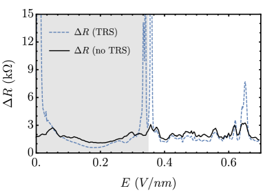 b
b 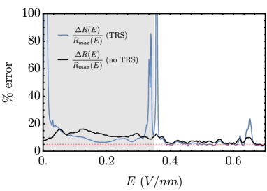
E.6 Topological Edge States
One advantage of our exact solution of the LB equation is that it makes no assumptions on the form of the matrix, and hence our experimentally determined matrix is an exact representation of the data. Furthermore, performs very well when predicting the values of other resistances. For these reasons, the full matrix serves as an accurate and complete description of the edge physics of the TDBG sample.
We would now like to use our matrix to show that the edge states of gapped TDBG at large enough have the properties we associate with topological phases. Firstly, we expect an insensitivity to impurities, defects of the edge, or more generally any change of parameter that does not change the bulk mirror Chern number. In our experiment, the transverse electric field is an excellent candidate. Once the gap is opened at , increasing the field further does not change the Chern number although it does have a strong effect on the band structure. A signature of the topological origin of the edge states is their insensitivity to in the gapped regime. A simple but powerful way to show this is to study how the whole matrix changes with . We consider the following quantity
| (40) |
which compares to by averaging the squared difference of every entry of the two matrices. This is related to the Frobenius norm, but divided by the number of off-diagonal entries so does not scale with the number of terminals. We chose as the field for comparison because it is the furthest into the gapped phase. We plot as a function of in Fig. 4f of the Main Text. We find that once the gap is open (), decays quickly and remains close to zero. This shows that the entire matrix, which fully characterizes the edge states, is essentially constant in the gapped phase and is thus insensitive to the transverse field. We contrast this case with non-topological edge states, like those on the zigzag edge of Bernal bilayer graphene which are gapped out by edge disorder or very large fields. We find the opposite behavior in our samples, which suggests nontrivial topology. Another strong comparison is to TDBG at V/nm where the system is a bulk conductor. We see strong variation in , signaling high sensitivity to . This contrasts the topological insulator phase.
We now discuss another measure of the edge states to assess the topology which generalizes the total conduction () discussed by Büttiker[26, 25]. We define this order parameter (as in Eq. 3) by
| (41) |
which is a sum over all the off-diagonal elements of . Intuitively, this corresponds to the total edge-to-edge transmission. In a topologically trivial insulator, edge states — if they exist — are not protected, and will be a small, non-quantized number which is sensitive to disorder, applied fields, and edge perturbations. In Fig. 4, we see that in the topological phase. This robust, nonzero value provides plausiblility of the survival of topological edge states, but fewer than would be expected from the bulk valley Chern number (including spin). Hence, quantitatively diagnoses the topology of the edge and shows that the bulk-boundary correspondence remains partially intact despite the edge symmetry-breaking. Another striking feature of Fig. 4f is the divergence in as V/nm where the gap closes. Because is a 1D (edge) conductivity, the closing of the gap creates a finite 2D (bulk) conductivity which sends . Mathematically, this arises in our formalism due to the pseudo-inverse of the resistance matrix. A bulk conductor reduces the resistance, leading to some singular values of approaching zero. This creates a divergence in the pseudo-inverse.
In topological insulators, we expect to have a robust, nonzero value. To illustrate this, let us consider the case of a perfectly clean QSH insulator with mirror Chern number , meaning that there is one chiral edge state for each spin, and they propagate with opposite chiralities. These states are topologically protected from scattering, so weak disorder will not affect them. This system is described by
| (42) |
which describes perfect transmission between neighboring terminals in both directions. Note that should be understood mod . Concretely, for , takes the form
| (43) |
We emphasize that because there are two edge states ( corresponds to a pair of counter-propagating edge states, e.g. one chiral state and one anti-chiral state), the columns of sum to 2. Hence for a probabilistic interpretation of as a scattering matrix, we must divide it by . To compute , we use the fact that all column sums are equal to 2, so
| (44) |
which explains the normalization we have chosen in Eq. 3. Note that in this case, is quantized in multiples of the conductance quantum. In a more realistic sample, there may be weak transmission across more distant terminals, but the columns sums of will still be equal to the number of edge states, up to uncertainties in measurements. (Column sums of less than the number of edge states implies scattering.) Similarly, topological edge states are protected from weak disorder and back-scattering. Thus, although is generically less structured than Eq. 42, is still expected to be fairly well quantized.
However, in TDBG, the situation is more complicated because the valley symmetry protecting the topological index is expected to be broken on the edge because it arises from the geometric moiré pattern. This differs from the QSH model where spin conservation protects the mirror Chern number and is not broken on the edge. As such, some back-scattering is expected, and indeed it is a priori not at all clear that any edge states would survive. However, we find in our experiments that reaches a finite, nonzero value in the gapped phase of approximately one quarter of the conductance we would expect from a with a spin degeneracy, as shown in Fig. 4f of the Main Text.
Lastly, we will show that is a natural observable in the LB formalism because it is an invariant under a discrete gauge symmetry corresponding to the arbitrary labeling of terminals which amounts to a permutation symmetry of the LB equation. Under a relabeling of the terminals where is a permutation of the numbers , there is a corresponding transformation of the conductance matrix: where , and similarly . We remark that permutation transforms of this type simply permute the diagonal elements of among themselves. This is consistent with all diagonal elements being unobservable. Because the physics of the edge is invariant under this relabeling, any well-defined order parameter of must be invariant under . We now show that satisfies this requirement. One simple way is to rewrite using the vector with all entries equal to . We find
| (45) |
The trace term is invariant under using the cyclicity property, and the fact that is orthogonal. The first term is invariant because , i.e. is an eigenvector of all permutations matrices because all its entries are the same. Note that the diagonal entries of cancel from Eq. 45.
Appendix F A Comparative Analysis of Bernal Bilayer Graphene
In this Appendix, we briefly introduce Bernal bilayer graphene[34, 29, 30] from the perspective of valleytronics[35]. We emphasize that there is no bulk valley symmetry in Bernal graphene, and hence there is not a bulk valley Chern number to protect edge states. Hence it is important to distinguish TDBG as a topologically protected state, whereas Bernal graphene is not. Indeed, Fig. 3b of the Main Text shows a monotonic increase in the longitudinal resistance as a function of , indicating a trivial insulator.
However, Bernal graphene does have strongly peaked Berry curvature with opposite sign in the and valleys. The cancellation of the Berry curvature causes the global Chern number to vanish, but there are still non-topological edge states that appear because the Berry curvature in each valley is large. For an armchair termination on cylinder boundary conditions, no edge states appear because the valleys are projected onto each other and cancel, but on zigzag terminations which do not project the valleys onto each other, edge states do appear in the spectrum[34]. However, these edge states are not topological and can be removed by edge perturbations.
We can also understand the local lack of stability of the Bernal edge states by calculating their characteristic localization length . Recall that the low energy behavior of Bernal graphene is a quadratic band touching[29] with a Berry phase of . When applied electric fields open a gap of , as is reachable by experiment, we can estimate the spread of the Berry curvature from the quadratic band touching using where is the Fermi velocity of graphene and is the hopping parameter. This gives an estimate of the characteristic momentum scale , or a real space length of . Edge roughness on this order will gap the non-topological edge states.
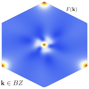
In comparison, we now calculate the Berry curvature of TDBG in the topological phase at using Eq. 16 (see Fig. S8). We find that the characteristic momentum scale of the Berry curvature is , giving a real space length scale of approximately 10 moiré periods. At , this is approximately . The increased delocalization of the edge states in TDBG explains their survival in our samples, despite the breakdown of the valley symmetry on the edge. Because the edge states are extended over many moiré periods, they are less sensitive to the edge termination, and retain the global symmetry-enforced topological protection of the bulk valley Chern number. Our calculations of agree at orders of magnitude with other heuristics of edge states localization, such as band flatness: where is the bandwidth, is the band gap, and is the characteristic length scale. For Bernal stacked graphene, , eV, and meV lead to nm.
