Electronic controllable broadband and robust terahertz surface plasmon-polaritons switch based on hybrid ITO waveguide coupler
Abstract
The surface plasmon-polaritons (SPPs) switch is the key element of the integrated devices in optical computation and terahertz (THz) communications. In this paper, we propose a novel design of THz SPPs switch based on quantum engineering. Due to the robustness of coherent quantum control technique, our switch is very robust against with perturbations of geometrical parameters and presents a good performance at on-state (and off-state) from 0.5 THz to 0.7 THz. The on-state and off-state of our device can be controlled by the external voltage. We believe this finding will be the great improvement for the integrated optical computing and THz communications.
pacs:
42.82.Et, 42.81.Qb, 42.79.Gn, 32.80.XxI Introduction
Terahertz (THz) Surface plasmon-polaritons (SPPs) is the most active research area in optical integrated device, due to the unique features of SPPs in relative smaller wavelength, energy confinement and field enhancement Liu2014 ; Williams2008 . THz SPPs devices are widely used in THz communications and THz information processing. Optical switch is the deice which can select the path of light propagation according to ’on-state’ and ’off-state’, which is the fundamental element in optical communications Mellette2016 ; Guo2019 and optical computing Seok2019 ; Yu2013 ; Hwang2017 . Combining with advantages of THz SPPs device and optical switch device, controllable THz SPPs switch has a large potential applications on THz communications and computation. Currently, there are few papers working on this idea, such as light-controlled THz SPPs device Cao2018 and THz switches based on graphene Luo2017 .
Most recently, there are two remarkable papers which proposed broadband and robust THz SPPs waveguide coupler based on coherent quantum control Huang20201 ; Huang20191 . The technique of coherent quantum control can be broadly used in many-body physics Huang20192 , waveguide coupler Huang20193 and graphene SPPs waveguide coupler Huang2018 . Due to the robustness of coherent quantum control, the especial curved SPPs waveguide coupler Huang20201 ; Huang20191 can completely transfer the energy of SPPs from input to output waveguide with wide working band and insensitivity to the perturbations of geometrical parameters. However, the previous researches Huang20201 ; Huang20191 can not control the output path of SPPs. The light-controlled THz SPPs device Cao2018 is not robust against geometrical parameters and only can operate in the narrowband. The terahertz switch based on graphene Luo2017 can operate at broadband, however, their device is not robust against geometrical parameters and this design of ’on-state’ (or ’off-state’) propagates (or not propagates) along with single SPPs waveguide. Thus, their device can not work as optical switch array for optical computing and can not controllable switch optical path. Besides, the fabrication of graphene sheet is much complex comparing to our design.
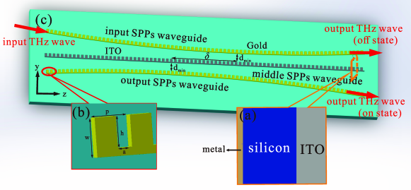
In this paper, we propose the device based on especial curved SPPs waveguide coupler inserted the hybrid indium tin oxide (ITO) waveguide in the middle of two metallic waveguides, as shown in Fig. 1, where the top waveguide functions as the input port and output port in ’off-state’ and the bottom one is the output port in ’on-state’. The hybrid ITO waveguide is the sandwiched structure with ITO layer, layer and metallic layer with several hundred nanometers. When we apply the external voltage on the metallic layer, ITO layer with very low conductivity can be considered as the insulating layer Li2019 . When the external voltage is not apply on the metallic layer, the ITO layer has high conductivity and can hold SPPs in THz region as the same as sliver and gold Franzen2008 .
Due to this unique feature of the ITO layer, we can apply the external voltage to control the conductivity of ITO corresponding to ’on-state’ and ’off-state’. The ’on-state’ without applying external voltage (ITO layer with high conductivity) can be considered as the three SPPs waveguide coupler. Thus, the energy of SPPs can completely transfer form input to output SPPs waveguide. Our device on the ’off-state’ with applying external voltage (ITO layer with very low conductivity) can be consider as two SPPs waveguide coupler without middle SPPs waveguide. Therefore, the distance between input and output waveguide becomes much larger and coupling strength between input and output waveguide turns much lower. The energy of SPPs confines in the input waveguide along with propagation.
In this paper, we firstly propose a typical example design (see Fig. 1) for our SPPs switch coupler and we illustrate the function of our switch according to ’on-state’ and ’off-state’ based on numerical calculations of SPPs coupler equation, as shown in Fig. 2. In section III, we further proof that our device is the robust against perturbations of geometrical parameters (, , and ) for both ’on-state’ and ’off-state’ (see Fig. 3). Besides, we demonstrate that our switch can operate at broad bandwidth, as shown in Fig. 4.
II Model and Device
Our device consists with three SPPs waveguide with special curved input and output SPPs waveguides (see Fig. 1). The input/middle/output SPPs waveguide has the , , and , as shown in Fig. 1 (b). It is already known that the period structure of SPPs waveguide can confine the SPPs in the THz region Zhang2018 ; Liu2014 and the SPPs’ transfer on curved waveguide is almost identical to straight case Pandey2013 ; Cui2013 , therefore, we can ignore the difference of the coupling strength induced by the curved configuration. The input/output SPPs waveguide is made of metallic layer and has the special curved configuration. The middle SPPs waveguide is the straight configuration with the sandwiched structure (the the ITO layer, the silicon layer and metallic layer), as shown in Fig. 1 (a).
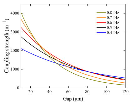
The coupling strength between two adjacent SPPs waveguides exponentially decreases along with the distance between two SPPs waveguide and this relationship is consist with coupled mode theory (CMT) Huang20201 ; Huang20191 ; Haus1991 and simulation results (see Fig. 5). The special-curved parameters of the SPPs waveguide coupler are total device length , circular radius , the minimum distance between input/output and middle waveguide and distance mismatch , as shown in Fig. 1 (c). The special curved configuration of input/output SPPs waveguide comes from a well-known coherent quantum control, called Stimulated Raman adiabatic passage (STIRAP) which has already shown the application in the SPPs waveguide coupler Huang2018 ; Huang20201 ; Huang20191 .
When there is no external voltage on the metal of middle SPPs waveguide (’on-state’), the ITO layer has very high conductivity considering as the gold layer. Thus the energy of SPPs can completely transfer from input to output SPPs waveguide via middle SPPs waveguide. When we apply the external voltage on the metal of middle SPPs waveguide (’off-state’), the ITO layer becomes ultra-low conductive. Therefore, the middle waveguide can not confine the SPPs, in other words, the coupling only happens between top and bottom SPPs waveguides. The distance between top and bottom SPPs waveguides is much larger comparing with ’on-state’. Thus, the energy of SPPs hardly transfer from top to bottom SPPs waveguide and confines in the input waveguide along with propagation.
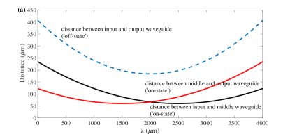
In order to demonstrate our idea, we present the distance configuration for ’on-state’ and ’off-state’ respectively, as shown in Fig. 2 (a). In the ’on-state’, the ITO waveguide with high conductivity can transfer the SPPs and the input and output waveguide can have the coupling via middle ITO waveguide. The black (red) solid line is the ’on-state’ of distance between input and middle (middle and output) waveguide. In the ’off-state’, the ITO waveguide with very low conductivity can not confine and hold the energy SPPs. Therefore, there is only the direct coupling between input and output waveguide. After that, it is already shown that the energy of SPPs evolves along with propagation , which is satisfied with SPPs waveguide coupling equation Huang20201 ; Huang20191 , such as
| (1) |
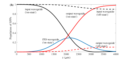
where , and are the SPPs amplitude of input, middle and output waveguides. The power of input/middle/output SPPs waveguide are . and are the coupling strengths of input/middle and middle/output SPPs waveguides. Therefore, we can numerically calculate the evolution of SPPs energy along with the propagation based on the coupling strengths between adjacent SPPs waveguides, as shown in Fig. 2 (b). As we can see that the energy of SPPs can completely transfer (more than 98 ) from input to output waveguide via middle waveguide (see the solid lines in Fig. 2 (b)) in the ’on-state’ configuration. In the ’off-state’ configuration, there is only few energy (less than 8 ) of SPPs transfer from input to output waveguide, due to the low direct coupling strength between input and output waveguide with low conductivity of middle SPPs waveguide.
III Robust and broadband switch
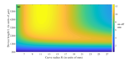
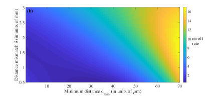
In this section, we demonstrate that our device is the robustness against the geometrical parameters length , curve radius , distance mismatch and minimum distance by using the SPPs coupler equations for both ’on-state’ and ’off-state’. Robustness against the geometrical parameters is a large advantage for the device fabrication, which largely increases the error suffering during the processing of fabrication and robustness hugely decreases the cost of device, due to not requirement of high precise equipment. In order to measure the performance of our switch in the same configuration, we introduce the on-off rate with , which the ’on-state’ divided by ’off-state’ of final SPPs energy of output waveguide to measure the energy difference of ’on-state’ and ’off-state’. Our ’on-state’ and ’off-state’ are separated by input and output waveguides (two different light pathway), therefore, if on-off rate is higher than 10, we can easily separate ’on-state’ and ’off-state’ by SPPs energy difference. The Fig. 3 demonstrates the on-off rate against varying different geometrical parameters. As we can see from the Fig. 3, we can easily obtain a large and continuous area of high on-off rate (higher than 10) with different geometrical parameters. Therefore, we can claim that our device is robust against the perturbations of geometrical parameters (such as the device length , curve radius , distance mismatch and minimum distance ).
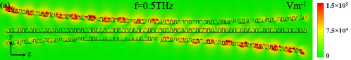
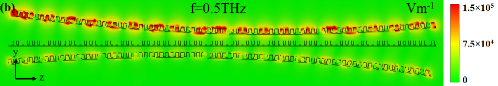
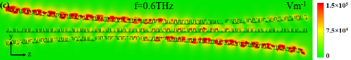
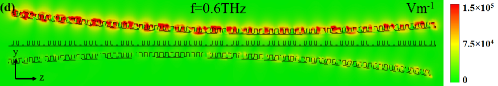
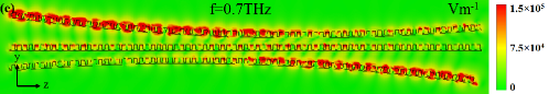
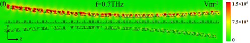
Furthermore, we employ the numerical software to full wave simulate the our switch based on different input frequencies. Fig. 4 (a) (c) (e) are the ’on-state’ for different frequencies and remaining figures are the ’off-state’ corresponding to the frequencies. As we can see that our device have a good performance both on ’on-state’ and ’off-state’ at frequencies from 0.5 THz to 0.7 THz in our this specific example configuration. When the frequencies are smaller than 0.5 THz, the ’off-state’ of our device do not have a good performance and too much power can be transferred to output waveguide, because the coupling strength becomes larger along with frequency decreasing with large gap (see the appendix Fig. 5). As we can see from the appendix Fig. 5, the coupling strength becomes much smaller at 0.8 THz when the gap is 60 . Therefore, the ’on-state’ of our device are not good at frequencies larger than 0.7 THz and coupling strengths are too small to support SPPs energy from input to middle SPPs waveguide.
IV Conclusion
In this paper, we propose a novel design of broadband and robust THz SPPs switch based on waveguide coupler embedded the coherent quantum control. From our example configuration, our switch is robust against the geometrical parameters, including the device length , curve radius , distance mismatch and minimum distance . Furthermore, we demonstrate the broadband performance of our switch from 0.5 THz to 0.7 THz for both ’on-state’ and ’off-state’. We believe this funding will be the great improvement for the integrated optical computation and THz communication.
Appendix
Due to the complicated boundary conditions, it is very hard to obtain the mode profile of the SPPs waveguides in the analytical solution, thus, analytical solving the relationship between coupling strength and gap between two SPPs waveguides is complicated. Therefore, we employs the full-wave simulation of two parallel SPPs waveguides to obtain the relationship between coupling strength and gap between two SPPs waveguides (see Fig. 5), which is consistent with the exponential relationship by coupled mode theory predicting Haus1991 .
Acknowledgements
This work acknowledges funding from National Key Research and Development Program of China (2019YFB2203901); National Science and Technology Major Project (grant no: 2017ZX02101007-003); National Natural Science Foundation of China (grant no: 61565004; 61965005; 61975038; 62005059; 62075248); National Key RD Program of China (Grant No. 2017YFB0405400; 2020YFB2001903). the Science and Technology Program of Guangxi Province (grant no: 2018AD19058). W.H. acknowledges funding from Guangxi oversea 100 talent project; W.Z. acknowledges funding from Guangxi distinguished expert project.
References
- (1) X. Y. Liu, Y. J. Feng, K. Chen, B. Zhu, J. M. Zhao and T. Jiang, “Planar surface plasmonic waveguide devices based on symmetric corrugated thin film structures,” Opt. Express., vol. 22, no. 17, pp. 20107-20116, Aug. 2014.
- (2) C. R. Williams et al., “Highly confined guiding of terahertz surface plasmon polaritons on structured metal surfaces,” Nat Photonics., vol. 2, no. 3, pp. 175-179, Feb. 2008.
- (3) W. M. Mellette et al., “A Scalable, Partially Configurable Optical Switch for Data Center Networks,” J Lightwave Technol., vol. 35, no. 2, pp. 136-144, Jan. 2017.
- (4) X. Q. Guo et al., “Scalable Nonblocking 4 x 4 Silicon Optical Switch Based on Dual-Microring Resonators,” Ieee Photonic Tech L., vol. 31, no. 5, pp. 397-400, Mar. 2019.
- (5) T. J. Seok et al., “Wafer-scale silicon photonic switches beyond die size limit,” Optica., vol. 6, no. 4, pp. 490-494, Apr. 2019.
- (6) R. X. Yu et al., “A scalable silicon photonic chip-scale optical switch for high performance computing systems,” Opt Express., vol. 21, no. 26, pp. 32655-32667, Dec. 2013.
- (7) H. Y. Hwang et al., “Flip chip packaging of digital silicon photonics MEMS switch for cloud computing and data centre,” IEEE Photon. J., vol. 9, no. 3, pp. 1-10, June. 2017.
- (8) L. D. Cao and Y. Zhang, ”Light controlled surface plasmon polaritons switch based on a gradient metal grating,” Opt Commun., vol. 424, pp. 103-106, Oct. 2018.
- (9) L. B. Luo et al., “Actively controllable terahertz switches with graphene-based nongroove gratings,” Photonics Res., vol. 5, no. 6, pp. 604-611, Dec. 2017.
- (10) W. Huang et al., “Quantum Engineering Enables Broadband and Robust Terahertz Surface Plasmon-Polaritons Coupler,” Ieee J Sel Top Quant., vol. 27, no. 2, pp. 1-7, Mar. 2020.
- (11) W. Huang et al., “Robust and broadband integrated terahertz coupler conducted with adiabatic following,” New J Phys., vol. 21, no. 11, pp. 113004, Nov. 2019.
- (12) W. Huang et al., “Population transfer via a dissipative structural continuum,” Phys Rev A., vol. 100, no. 6, pp. 063430, Dec. 2019.
- (13) W. Huang, Lay-Kee. Ang and Elica Kyoseva, “Shortcut to adiabatic light transfer in waveguide couplers with a sign flip in the phase mismatch,” J Phys D Appl Phys., vol. 53, no. 3, pp. 035104, Nov. 2019.
- (14) W. Huang et al., “Adiabatic control of surface plasmon-polaritons in a 3-layers graphene curved configuration,” Carbon., vol. 127, pp. 187-192. Feb. 2018.
- (15) S. M. Li et al., “Nanometre-thin indium tin oxide for advanced high-performance electronics,” Nat Mater., vol. 18, no. 10, pp. 1-7, Oct. 2019.
- (16) S. Franzen, ”Surface plasmon polaritons and screened plasma absorption in indium tin oxide compared to silver and gold,” J Phys Chem C., vol. 112, no. 15, pp. 6027-6032, Apr. 2008.
- (17) Y. Zhang et al., “Terahertz spoof surface-plasmon-polariton subwavelength waveguide,” Photonics Res., vol. 6, no. 1, pp. 18-23, Jan. 2018.
- (18) S. Pandey, B. Gupta and A. Nahata, ”Terahertz plasmonic waveguides created via 3D printing,” Opt Express., vol. 21, no. 21, pp. 24422-24430, Oct. 2013.
- (19) T. J. Cui and X. P. Shen, ”THz and microwave surface plasmon polaritons on ultrathin corrugated metallic strips,” Terahertz Sci. Technol., vol. 6, no. 2, pp. 147-164, June. 2013.
- (20) H. A. Haus and W. P. Huang, ”Coupled-Mode Theory,” P Ieee., vol. 79, no. 10, pp. 1505-1518, Oct. 1991.