Multiterminal Quantized Conductance in InSb Nanocrosses
Abstract
By studying the time-dependent axial and radial growth of InSb nanowires, we map the conditions for the synthesis of single-crystalline InSb nanocrosses by molecular beam epitaxy. Low-temperature electrical measurements of InSb nanocross devices with local gate control on individual terminals exhibit quantized conductance and are used to probe the spatial distribution of the conducting channels. Tuning to a situation where the nanocross junction is connected by few-channel quantum point contacts in the connecting nanowire terminals, we show that transport through the junction is ballistic except close to pinch-off. Combined with a new concept for shadow-epitaxy of patterned superconductors on nanocrosses, the structures reported here show promise for the realization of non-trivial topological states in multi-terminal Josephson Junctions.
Combining intrinsic confinement and high crystal quality, III-V semiconductor nanowires (NWs) have constituted an important experimental platform for mesoscopic physics and quantum devices for the past two decades Thelander et al. (2006); Doh et al. (2005); Nadj-Perge et al. (2010); Hofstetter et al. (2009). Renewed interest was triggered by proposals for engineering exotic topological phases in strong spin-orbit interaction (SOI) one-dimensional (1D) NWs with proximity induced superconductivity Oreg et al. (2010); Lutchyn et al. (2010). This led to significant theoretical works and experimental efforts in device engineering and material developments of hybrid semiconductor/superconductor structures Lutchyn et al. (2018); Krogstrup et al. (2015). In addition, proposals for realizing quantum operations by braiding the world lines of non-abelian Majorana quasi-particles in networks of 1D hybrid nanowires Alicea et al. (2011) create a need to extend the conventional linear NW platform towards branched hybrid structures. Different schemes are being developed towards planar NW networks Gooth et al. (2017); Friedl et al. (2018); Krizek et al. (2018); Vaitiekenas et al. (2018); Aseev et al. (2019) and vapor-liquid-solid NW growth has been extended to simpler branched structures either by changing the growth directions during growth Lao et al. (2002); Dick et al. (2004); Plissard et al. (2013); Krizek et al. (2017); Jespersen et al. (2018) or by merging non-parallel NWs grown from tilted substrate facets Dalacu et al. (2013); Gazibegovic et al. (2017). The high mobility and strong SOI make indium antimony (InSb) the optimal candidate for transport measurements, however, branched InSb NW structures and nanocrosses have not so far been reported using molecular beam epitaxy (MBE) – traditionally leading to crystals with the lowest impurity concentration.
Here, we demonstrate controlled synthesis of InSb nanocrosses (NCs) using MBE, where the challenge of initiating InSb growth is overcome using a two-step procedure, beginning with a short segment of InAs supporting the subsequent InSb NW. A NC geometry is enabled by growing NWs from facing, non-parallel facets. We map the conditions for NC formation in terms of relative catalyst position, axial growth rates, and radial growth of InSb NW. Structural characterization using transmission electron microscopy (TEM) confirms a single-crystal Zinc-Blende (ZB) phase across the InSb NC. Further, we study the low-temperature electron transport of the InSb NCs with local gate-control of each individual terminal. Each terminal exhibits quantized conductance, and from analysis of the combined transport through two quantized constrictions we infer ballistic transport also over the NC junction, except for global gate potentials close to pinch-off. Finally, we demonstrate a new concept for merging the NC geometry with pre-defined substrate structures to enable in situ patterning of epitaxial superconductors, which have been shown to substantially enhance the performance of hybrid devices Khan et al. (2020); Carrad et al. (2020); Heedt et al. (2020).
I Results and Discussion
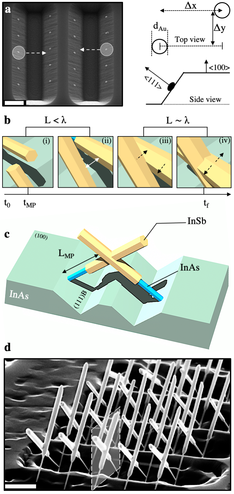
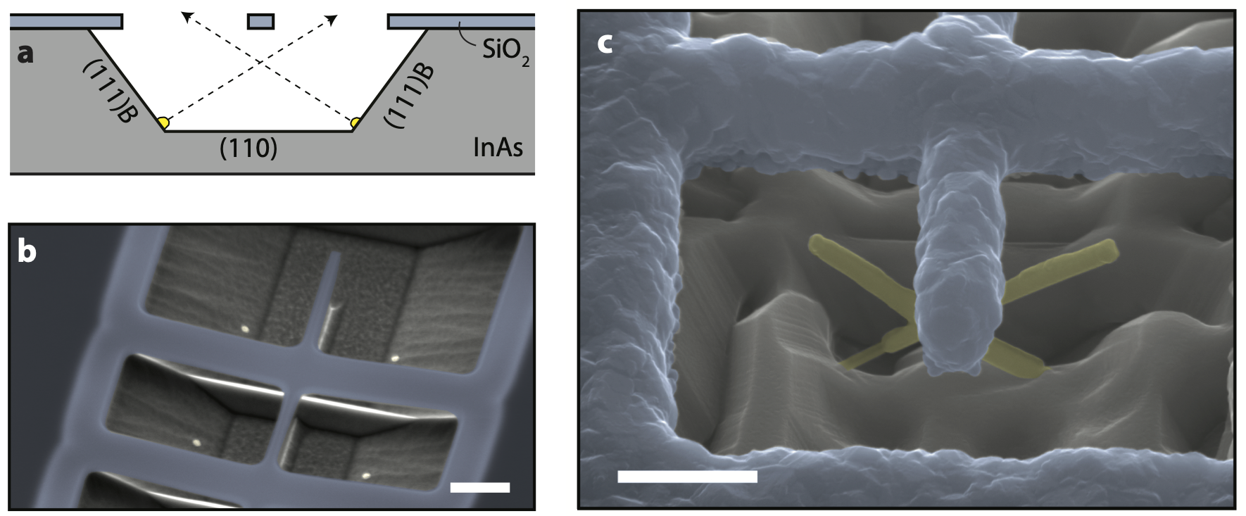
Growth of InSb Nanocrosses. The growth of InSb NCs was enabled using InAs (100) substrates containing (111)B faceted trenches, which were fabricated by chemical etching following along the lines of Ref. Khan et al. (2020). Au catalyst particles with relative lateral distances , were defined on opposing facets using electron beam lithography. See Fig. 1a for a definition of the coordinate system and a scanning electron microscope (SEM) micrograph of a typical substrate before growth. The result of the final NW structure depends critically on the relation between y, the diameter of the supersaturated Au catalyst that defines the initial diameter of the InSb NW during axial growth, and the amount of radial growth when the NW reach to it’s final diameter . For the NWs meet “head-to-head” and the axial growth is interrupted preventing the formation of four-terminal crosses de Vries et al. (2019); Kang et al. (2017). This situation is discussed in the Supporting Information (S1-S6). For exceeding the final NW diameter , the two NWs remain separated, while for a finite off-set the resulting structure and the possibility of forming connected four-terminal crosses depends on the relation between , , , and . Here, refers to the time when the two catalyst particles pass each other at the closest point. The sequence is illustrated in Fig. 1b. Ideally, the growth front (the size of which is given by ) of the two NWs pass each-other with minimal separation thus, continuing axial growth while the simultaneous radial overgrowth eventually merges the two NWs epitaxially at the meeting-point. The final structure is schematically shown in Fig. 1c and a typical example of MBE grown NCs is presented in Fig. 1d.
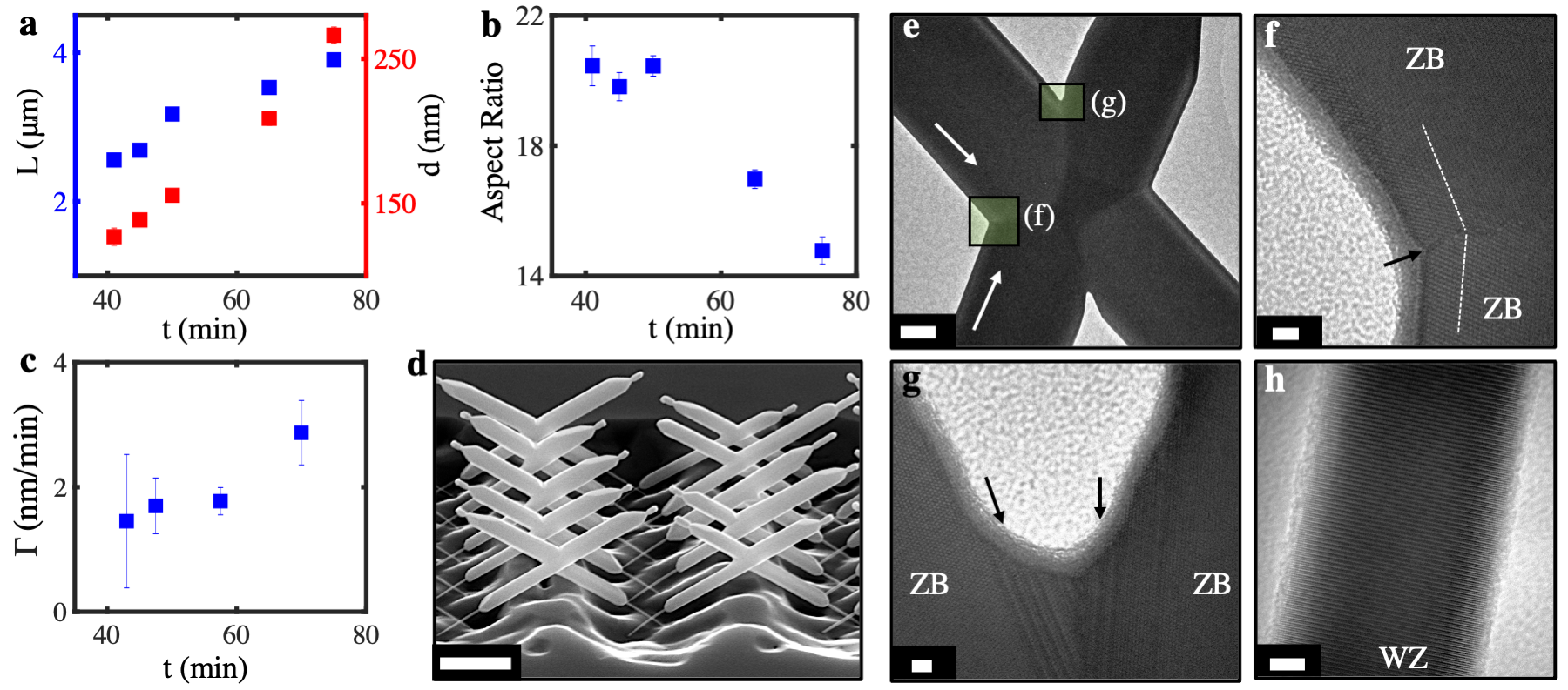
To find the optimal parameters for NC formation five growths of different growth-times between 41 and 75 minutes were performed, and Fig. 2a shows the measured average InSb lengths and final diameters from NWs grown in trenches (with m and pitch size of 970 nm between Au catalysts). Both length and diameter increase with time but while the diameter more than doubles in this time interval, the length only increases by a factor of 1.5. This trend is also evident from the decaying aspect ratio extracted in Fig. 2b. The InSb NW growth is initiated by axial growth via the liquid-solid transition, with an initial diameter , which is determined by the volume and contact angle of the Au particle at the point of supersaturation with In and Sb. After some time, the NW length becomes comparable to the incorporation limited diffusion length and adatoms cannot reach to the Au particle, initiating radial growth on the side facets. In general, radial growth can be divided into three stages: no radial growth (), transition stage (), and constant radial growth (). The extracted radial growth rate is presented in Fig. 2c from which is can be seen that the main part of the InSb growth resides in the transition stage for the studied growth times from 43 to 70 minutes (see Fig. 2c). Note that, the growth parameters were chosen to promote radial growth, rather than long NW with high aspect ratio, as this is required for the formation of high quality NCs.
Extrapolating the diameter in Fig. 2a to , we estimate a diameter of the growth front of and choosing , the growth fronts is expected to pass uninterrupted at . The length of the combined InAs/InSb NW at the meeting point with being the inclination angle of the (111)B facet, is determined by the position of the Au catalyst particles and was for our substrates. The InAs stem was grown to a length of leaving for the InSb to reach the meeting point (MP). As seen in Fig. 2a, the NWs reach this point after a growth time shorter than having then a diameter , and therefore, the NWs pass each other at the MP as separate structures. Figure 2d shows an example of a growth performed for leading to high throughput NCs formation. Here, the final length of the InSb NWs were m with diameter of nm and the radial overgrowth results in clear joining of the NW pairs into four-terminal NCs.
Structural TEM characterization is presented in Fig. 2(e-h) and further details are provided in Supporting Information S1. Figure 2e shows the overall structure of a NC (grown along the direction of the arrows) and confirms that all the four arms along with the merged region maintain the same crystal structure throughout. The high contrast structure in the middle region is a consequence of the difference in thickness of the structure. No stacking-faults or crystal defects were observed in the NC arms. Figure 2f shows a high-resolution image of the obtuse corner between the NWs. The ZB crystal phase is maintained also in the structure closest to the surface, which is grown radially from the side facets and responsible for the merging of the crystals. A twin-plane is observed at the point of merging, which we attribute to misalignment or different stacking order of the two phases. Correspondingly, Fig. 2g shows a high resolution image of the acute corner where multiple stacking faults are observed in the surface layers growh radially (arrows) presumably also caused by misalignment of the two crystals. These, however, only appear in the radially grown part of the crystal and do not propagate into the core of the wires. Figure 2h shows the high resolution (HR)-TEM image of wurtzite (WZ) InAs stem without any disorders. InAs stems get thinner with longer InSb growth time due to the As decomposition.
Low Temperature Transport Characterization. We now consider the low-temperature electrical properties of the MBE-grown InSb NCs. Previous studies of InAs Suyatin et al. (2008); Heedt et al. (2016); Rieger et al. (2016); Kang et al. (2013) and InSb NCs Plissard et al. (2013); Fadaly et al. (2017); Gazibegovic et al. (2017) have confirmed transport both along and between the two merged NWs, where both ballistic transport at high fields Fadaly et al. (2017) and phase-coherence Gazibegovic et al. (2017) have been demonstrated. A main reason for using branched nanostructures is the potential to individually gate control nanowire branches, thus enabling e.g. measurements of the local density of states Zhang et al. (2019), a control of the effective size of the scattering matrix in coherent multi-terminal junctions Riwar et al. (2016), or eventually braiding Majorana zero modes in topological junctions Alicea et al. (2011). So far, however, only global electrostatic gating has been demonstrated.
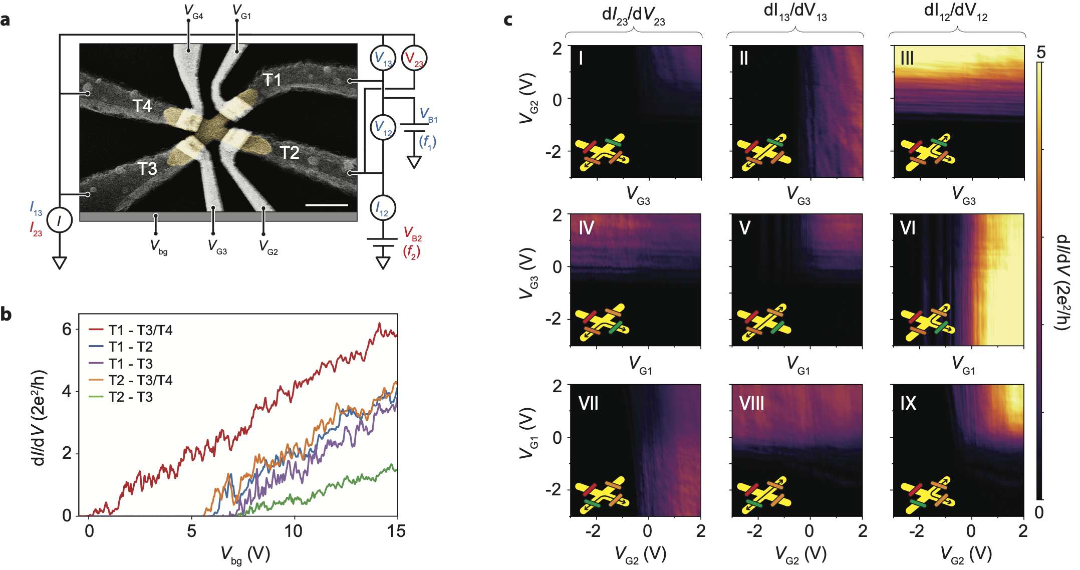
For device fabrication, NCs were located on the growth substrate using SEM and subsequently transferred using a manual micro-manipulator to highly doped Si substrates capped with of SiO2. Ohmic contacts to each terminal (denoted ) were defined by e-beam lithography and deposition of Ti/Al metals. Subsequently, 10 nm of was deposited using atomic layer deposition and four individual Ti/Au top gates (potentials ) were defined on the NC terminals. The gates overlap the electrodes and nm of the exposed InSb, and their separation is . Figure 3a shows an SEM micrograph of the device. The back-gate (), acts globally and in particular at the center of the cross. Terminals T3 and T4 were connected on the chip and most measurements had , keeping terminal in pinch-off.
Measurements were carried out either by a pair-wise two-terminal AC lock-in configuration with the unused terminals floating, or employing a three-terminal AC setup, as schematically shown in Fig. 3a allowing simultaneous measurements of all relevant combinations , , and (See Methods). Measurements were performed in a dilution refrigerator at an electron temperature . We note that Al is a superconductor at the measurement temperatures, however, no signatures of superconductivity were detected, presumably due to a disordered interface between InSb and the Ti/Al electrodes as further discussed below.
Figure 3b shows the back gate dependence of the conductance of individual connections T1 - T3/T4 (red), T2 - T3/T4 (orange), and T1 - T2 (blue) measured with the remaining terminals floating and top-gates grounded. For the purple and green traces the connections (T1-T3) and (T2-T3) were measured with to disconnects T4. In all cases, conductance increases with more positive , as expected for a -type semiconductor and the conductance values for is relatively high for such devices indicating low resistance Ohmic contact. The traces exhibit pronounced reproducible oscillations, which are attributed to conductance fluctuations due to phase coherence as commonly observed in NW devices at low temperatures Doh et al. (2005).
The threshold for T1-T3/T4 is , while it is shifted to 6V for T2-T3/T4, showing that acts non-uniformly on the terminals activating T2 at higher . Also, closing T4 (, purple trace), shifts to 6V suggesting that for transport is dominated by a local path T1-T4. Close to pinch-off transport is thus not spatially uniform. Except for T2-T3, however, the transconductances are similar for all combinations , and estimating the back-gate capacitance by a simplified model of a NW above a planar back gate Wunnicke (2006), we find a field effect mobility of 700 . This rough estimation disregards field focusing by the cross geometry and screening from electrodes and top-gates, but the value is comparable to the values reported for individual InSb NWs Gül et al. (2015).
Turning now to the gate control and capacitive cross-coupling of individual arms of the NC, we fix , and Fig. 3c shows the three simultaneously measured conductances (columns) vs. different pairs of top gates. The non-swept gates were kept at 2V, thus keeping the corresponding terminal open; the configuration for each panel is indicated by the icons. All top gates show a consistent threshold at and the maps qualitatively follow the expectations of a transistor network with little cross-coupling between the gates. Consider for example panels I-III, where (vertical axis) modulate the connection between T2 and T3 (panel I) and between T1-T2 (panel III), while is unaffected (panel II). Also, for panels I, V, IX on the diagonal, which show as a function of and , finite conductance is only obtained when both gates are at positive potential. Cross-coupling due to the geometric proximity distorts conductance features from horizontal/vertical and the largest effect is observed between and in panel IX exhibiting a cross-coupling. The main result of Fig. 3 is thus to establish the possibility for individually controlling the legs of the NC.
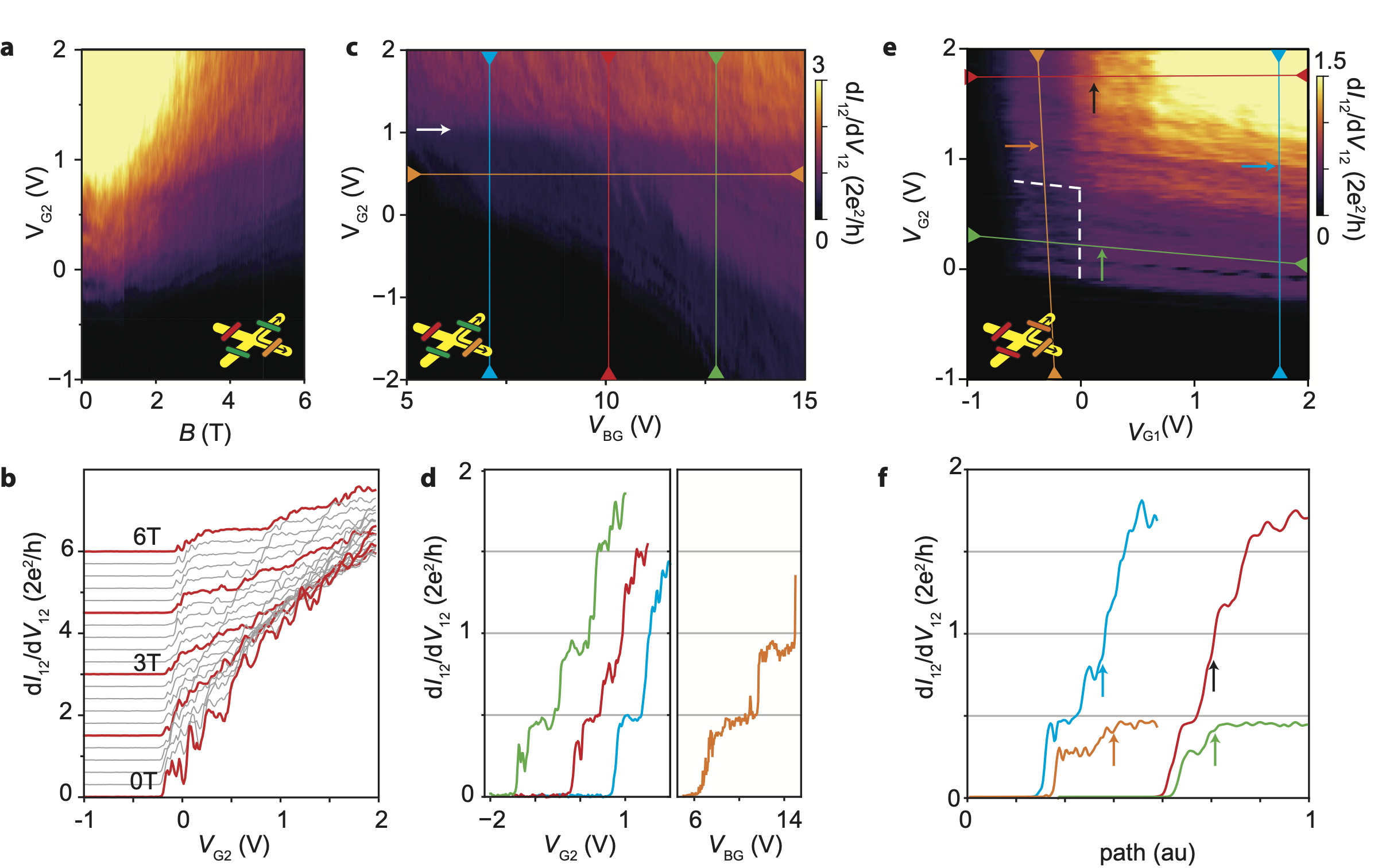
Although the gates act locally on the terminals of the cross and transport is coherent at low temperature, the measurements in Fig. 3c do not show clear quantized conductance presumably due to quantum interference and scattering dominating the transport. Previous studies of single nanowires van Weperen et al. (2013) and globally gated NCs Fadaly et al. (2017) have found that a magnetic field can suppress scattering and enhance the signatures of ballistic transport. Figures 4a,b show vs. perpendicular magnetic field and with (T1 and T3 fully open). thus control the main barrier for transport and for , increases in discrete steps of , the conductance of single, spin-split one-dimensional channels below the gate. This is further emphasized by the line-traces in Fig. 4b.
To study further the properties of the local barrier on the NC, Fig. 4c shows vs. and for . See Supporting Information S7(d,e) for the remaining gate combinations. In all cases, regions of quantized conductance are clearly observed confirming the ballistic 1D nature of the gate-defined constrictions of the NC terminals. Two distinct transitions are distinguishable; one nearly independent of (arrow in panel (c)), and others which are modulated by both and . We attribute these to spatially separated transport paths both acting as quantum point contacts; one located close to the top gate and thus unaffected by and the other closer to the bottom of the semiconductor terminal and thus affected by both gates. Figure 4d shows extracted traces at the positions in Fig. 4c indicated by arrows, highlighting the flatness of the plateaus and the effective doubling of the step height when simultaneously crossing transitions from both families (blue curve). Understanding of such complexity in the effective device geometry, observed even when back-scattering is suppressed by the magnetic field is important for interpreting and utilizing nanowire networks for complex quantum devices. Further insight of individual paths could potentially be gained through detailed analysis of the properties at finite bias or utilizing additional local gates, however, these are beyond the scope of this study.
The observation of quantized conductance shows that transport is ballistic at a length scale of the effective constriction induced by the top gates. Compared to previous studies, the possibility of introducing ballistic point contacts at the individual terminals allows further insight into the transport specifically through the crossing region. For two ballistic constrictions in series (QPC1 and QPC2), a fully diffusive transport in the intermediate NC will result in an ohmic addition to the total conductance while, in the case of a fully ballistic intermediate transport, . To this end Fig. 4e shows a measurement at and of vs. and while keeping T3 and T4 in pinch-off (). This adds the two ballistic constrictions at T1 and T2 in series. Consider first the red trace in panel f, extracted at . In this case, T2 is fully open, and the total conductance increases step wise upon gradually opening T1. The green trace shows a similar situation except T2 is now maintained at the first plateau. Interestingly, upon opening up T1, the conductance first shows a plateau at , as expected for an Ohmic (diffusive) addition of the two constrictions. However, upon further increasing , the conductance increases to and – as expected for ballistic transport between the two terminals – stays constant while increasing the number of channels in T1. A similar behavior is observed in the reverse situation, where T1 is open and channels are gradually added to T2 (blue and orange traces in Fig. 4f). Thus, transport between the two constrictions, i.e. through the merged NWs, appears ballistic except close to pinch off. The corresponding results from the other combinations of terminals are presented in Supporting Information S8 consistent with this scenario. A plausible scenario is that the first modes are located closer to the surface and thus subject to stronger scattering than at higher densities, where transport occur through the bulk of the NC.
In situ Shadow Patterning of Nanocrosses. The scattering in the junction, the need for high magnetic fields to observe quantized conductance of the constrictions, and the absence of proximity induced superconductivity from the evaporated Al leads, may be traced back to disorder related to the device processing. Replacing evaporation and post processing with growth of epitaxial superconductors is a well established method for avoiding disorder-related degradation of device performance Krogstrup et al. (2015). However the fragility of InSb is a challenge for devices based on InSb/Al epitaxial hybrids as all known etchings of Al also severely damages the InSb semiconductor and degrade device performance. Recently, in situ “shadow” approaches Carrad et al. (2020); Gazibegovic et al. (2017); Krizek et al. (2017); Khan et al. (2020); Heedt et al. (2020) have been developed allowing patterning of epitaxial superconductor growth, yielding reproducible transport characteristics and observations of ballistic transport at for single nanowires. These in situ shadow concepts, developed for single NWs, are however, incompatible with the NC geometry, where controlled shadows of the central junction region is required for most applications. Figure 5 demonstrates a new adaptation of the approach in Ref. Carrad et al. (2020) to accommodate the NC geometry. The substrates were prepared with shadow structures suspended over the trenches. The design features four 1m wide strips bridging each trench. These support a 150 nm wide cross-bar suspended along the middle of the trench. The cross-bar act as a shadow-structure for the junction of NC grown to have their merging point below the substrate surface plane. Figure 5a shows a schematic side view of the substrate and panel b shows a SEM micrograph of the substrate before the growth (see Methods for details). Figure 5c shows an example of a InSb NC grown below the cross-bar. Substantial overgrowth on the mask is also observed in this case, effectively widening the shadow bridge, and further optimization of growth parameters and/or bridge design is needed. The results, however, demonstrate the feasibility of this approach, and we expect that the electrical performance of the shadow crosses will increase similarly to the results reported for conventional nanowire devices fabricated by in situ shadow techniques Khan et al. (2020); Carrad et al. (2020).
II Conclusion
In conclusion, we have presented a detailed study of MBE grown InSb NCs. From the time-dependence of axial and radial growth of InSb NWs, we determined the combination of geometric and growth parameters optimal for NC growth featuring a coherent crystal structures. InSb NC devices were fabricated with individual electrostatic control of all terminals, each showing clear quantized conductance at low temperature and high magnetic fields. Analyzing the combined action of two point contacts connected in series through the cross, showed that inter-wire transport in the NC is quasi-ballistic except close to pinch-off, where signatures of diffusive transport occurs. Finally, we developed and demonstrated a shadow-technique allowing epitaxial growth of hybrid semiconductor/superconductor NCs with in situ shadow junctions aligned to the NC intersection point. The approach can be applied for any choice semiconductor and superconductor, but is demonstrated here for InSb/Al hybrid crosses. The technique is expected to dramatically reduce disorder-related scattering and thus be an important step towards clean quantum transport in complex multi-terminal nanowire devices.
III Methods
Substrate Fabrication and Nanocross Growth. InAs (100) 2-inch wafers are used for substrate fabrication. (111)B trenches are created on the substrate using and solution based wet-etching process, as discussed in Khan et al. (2020). Later, electron beam lithography is used for defining the position of the Au seed particles on the (111)B trenches with an offset for forming NCs. Post-exposure development is done using standard 1:3 MIBK: IPA solution. Electron beam evaporator with a rate of 1 Å/s is used for depositing Au thin layer. Subsequently, lift-off is performed using acetone dipping. Next, cleaning is done with 2 min of sonication with acetone, rinsing with IPA and milli-q water. Finally, 2 min oxygen plasma treatment is conducted to avoid resist residues on the substrate.
InSb NCs are grown using Veeco GEN II MBE system. Initially, substrate is annealed at 590 ∘C with arsenic over-pressure. Subsequently, InAs stem is grown typically for 12 min (prior to NC segment), where As/In flux ratio is maintained 9.78, resulting the length of the stems are 1.3- 1.6 m. Depending on the substrate geometry the growth time (length) of InAs stem is varied. Next, the As flux is terminated and Sb flux is introduced in the system maintaining continuous In flux. Consequently, InSb segments are grown on top of the stems using Sb/In flux ratio 4.3. The growth time of InSb segment is varied depending on the space between the catalysts and radial growth radial growth required to overcome this space to create NC, as discussed in the growth section above. Throughout the NW growth the substrate temperature is maintained to 447 ∘C (set temperature).
For hybridization of the NCs, Al deposition is performed in situ in the MBE growth chamber. After the NC growth, the substrate is cooled down to 36∘C. Usually, 8-10 hours is the waiting period before the temperature is reached and growth chamber is ready for Al deposition. Low temperature limits the adatom diffusion length and thermodynamically drives to form continuous Al thin film on InSb NW. Upon the temperature is reached, the deposition angle is adjusted with the Al source, which confirms the shadow region in the middle of the NC. Before unloading, 15 min of oxidization is performed to create passivation layer and avoid the Al dewetting issue in the elevated temperature.
Structural Characterization. The morphology of the NCs are characterized by SEM. Crystal structures and intersection of the NCs are characterized by TEM and HR-TEM of FEI Tecnai T20 G2 (200 kV of acceleration voltage, Thermionic LaB6/CeB6 e-beam source, point resolution of 0.24 nm, line resolution of 0.14 nm, and STEM resolution of 1.0 nm).
Electrical Measurements. The electrical setup is shown in Fig. 3(a). Terminals 1 and 2 are ac voltage biased with two incommensurable frequencies (indicated by blue and red colors), and both resulting ac currents are measured using lock-in detection at terminal 3 yielding and , where and are the local voltage drops measured separately with lock-in detection at the respective frequencies. The bias at is applied at the back of a current amplifier which measures the current at frequency thus yielding .
Fabrication of Shadow Bridges. Shadow bridges were fabricated along the lines of Ref. Carrad et al. (2020): 150 nm of SiOx were deposited by plasma enhanced chemical vapor deposition (PECVD) on InAs (100) substrates and patterned by EBL and HF etching into the pattern of bridges supporting the cross-bar for shadowing. Subsequently, the InAs trenches were etched using a separate EBL step and the same wet etchant as discussed before. Catalyst particles were defined by EBL on the facets as shown in Fig. 1. Careful alignment is required to ensure a NC junction forming directly below the shadow bar.
IV Supporting Information
The Supporting Information is available at: https://sid.erda.dk/share_redirect/B9S92R2aTL
V Author contribution
S.A.K, J-H.K. performed the MBE growth, material analysis and optimization supervised by P.K.; L.S, T.M. performed electrical measurements, analyzed the results, and developed the shadow concept supervised by T.S.J.; S.A.K, L.S. and T.S.J. wrote the manuscript with input from all authors.
VI Acknowledgement
S.A.K, J-H.K. and P.K. was funded by European Union Horizon 2020 research and innovation program under the Marie Skłodowska-Curie Grant No. 722176 (INDEED), Microsoft Quantum and the European Research Council (ERC) under Grant No. 716655 (HEMs-DAM). T.S.J was supported by research grants from Villum Fonden (00013157), The Danish Council for Independent Research (7014-00132), and European Research Council (866158). Authors thank to C. B. Sørensen for the maintenance of the MBE system.
References
- Thelander et al. (2006) C. Thelander, P. Agarwal, S. Brongersma, J. Eymery, L. F. Feiner, A. Forchel, M. Scheffler, W. Riess, B. J. Ohlsson, U. Goesele, and L. Samuelson, Mater. Today 9, 28 (2006).
- Doh et al. (2005) Y. Doh, J. van Dam, A. Roest, E. Bakkers, L. Kouwenhoven, and S. De Franceschi, Science 309, 272 (2005).
- Nadj-Perge et al. (2010) S. Nadj-Perge, S. M. Frolov, E. P. A. M. Bakkers, and L. P. Kouwenhoven, Nature 468, 1084 (2010).
- Hofstetter et al. (2009) L. Hofstetter, S. Csonka, J. Nygard, and C. Schoenenberger, Nature 461, 960 (2009).
- Oreg et al. (2010) Y. Oreg, G. Refael, and F. von Oppen, Phys. Rev. Lett. 105 (2010).
- Lutchyn et al. (2010) R. M. Lutchyn, J. D. Sau, and S. Das Sarma, Phys. Rev. Lett. 105 (2010).
- Lutchyn et al. (2018) R. M. Lutchyn, E. P. A. M. Bakkers, L. P. Kouwenhoven, P. Krogstrup, C. M. Marcus, and Y. Oreg, Nat. Rev. Mater. 3, 52 (2018).
- Krogstrup et al. (2015) P. Krogstrup, N. L. B. Ziino, W. Chang, S. M. Albrecht, M. H. Madsen, E. Johnson, J. Nygard, C. M. Marcus, and T. S. Jespersen, Nat. Mater. 14, 400 (2015).
- Alicea et al. (2011) J. Alicea, Y. Oreg, G. Refael, F. von Oppen, and M. P. A. Fisher, Nat. Phys. 7, 412 (2011).
- Gooth et al. (2017) J. Gooth, M. Borg, H. Schmid, V. Schaller, S. Wirths, K. Moselund, M. Luisier, S. Karg, and H. Riel, Nano Lett. 17, 2596 (2017).
- Friedl et al. (2018) M. Friedl, K. Cerveny, P. Weigele, G. Tutuncuoglu, S. Marti-Sanchez, C. Huang, T. Patlatiuk, H. Potts, Z. Sun, M. O. Hill, L. Guniat, W. Kim, M. Zamani, V. G. Dubrovskii, J. Arbiol, L. J. Lauhon, D. M. Zumbuhl, and A. Fontcuberta i Morral, Nano Lett. 18, 2666 (2018).
- Krizek et al. (2018) F. Krizek, J. E. Sestoft, P. Aseev, S. Marti-Sanchez, S. Vaitiekėnas, L. Casparis, S. A. Khan, Y. Liu, T. Stankevič, A. M. Whiticar, et al., Physical review materials 2, 093401 (2018).
- Vaitiekenas et al. (2018) S. Vaitiekenas, A. M. Whiticar, M. T. Deng, F. Krizek, J. E. Sestoft, C. J. Palmstrom, S. Marti-Sanchez, J. Arbiol, P. Krogstrup, L. Casparis, and C. M. Marcus, Phys. Rev. Lett. 121 (2018).
- Aseev et al. (2019) P. Aseev, G. Wang, L. Binci, A. Singh, S. Marti-Sanchez, M. Botifoll, L. J. Stek, A. Bordin, J. D. Watson, F. Boekhout, D. Abel, J. Gamble, K. Van Hoogdalem, J. Arbiol, L. P. Kouwenhoven, G. de Lange, and P. Caroff, Nano Lett. 19, 9102 (2019).
- Lao et al. (2002) J. Lao, J. Wen, and Z. Ren, Nano Lett. 2, 1287 (2002).
- Dick et al. (2004) K. Dick, K. Deppert, M. Larsson, T. Martensson, W. Seifert, L. Wallenberg, and L. Samuelson, Nat. Mater. 3, 380 (2004).
- Plissard et al. (2013) S. R. Plissard, I. Van Weperen, D. Car, M. A. Verheijen, G. W. Immink, J. Kammhuber, L. J. Cornelissen, D. B. Szombati, A. Geresdi, S. M. Frolov, et al., Nature nanotechnology 8, 859 (2013).
- Krizek et al. (2017) F. Krizek, T. Kanne, D. Razmadze, E. Johnson, J. Nygard, C. M. Marcus, and P. Krogstrup, Nano letters 17, 6090 (2017).
- Jespersen et al. (2018) T. S. Jespersen, P. Krogstrup, A. M. Lunde, R. Tanta, T. Kanne, E. Johnson, and J. Nygard, Phys. Rev. B 97, 041303 (2018).
- Dalacu et al. (2013) D. Dalacu, A. Kam, D. G. Austing, and P. J. Poole, Nano letters 13, 2676 (2013).
- Gazibegovic et al. (2017) S. Gazibegovic, D. Car, H. Zhang, S. C. Balk, J. A. Logan, M. W. de Moor, M. C. Cassidy, R. Schmits, D. Xu, G. Wang, et al., Nature 548, 434 (2017).
- Khan et al. (2020) S. A. Khan, C. Lampadaris, A. Cui, L. Stampfer, Y. Liu, S. J. Pauka, M. E. Cachaza, E. M. Fiordaliso, J.-H. Kang, S. Korneychuk, et al., ACS nano (2020).
- Carrad et al. (2020) D. J. Carrad, M. Bjergfelt, T. Kanne, M. Aagesen, F. Krizek, E. M. Fiordaliso, E. Johnson, J. Nygard, and T. S. Jespersen, Adv. Mater. 32 (2020).
- Heedt et al. (2020) S. Heedt, M. Quintero-Pérez, B. Francesco, A. Fursina, N. van Loo, G. P. Mazur, M. Nowak, M. Ammerlaan, K. Li, S. Korneychuk, J. Shen, M. van de Poll, G. Badawy, S. Gazibegovic, K. van Hoogdalem, E. P. A. M. Bakkers, and L. Kouwenhoven, arXiv:2007.14383 (2020).
- de Vries et al. (2019) F. K. de Vries, M. L. Sol, S. Gazibegovic, R. L. op het Veld, S. C. Balk, D. Car, E. P. Bakkers, L. P. Kouwenhoven, and J. Shen, Physical Review Research 1, 032031 (2019).
- Kang et al. (2017) J.-H. Kang, M. Galicka, P. Kacman, and H. Shtrikman, Nano letters 17, 531 (2017).
- Suyatin et al. (2008) D. B. Suyatin, J. Sun, A. Fuhrer, D. Wallin, L. E. Froberg, L. S. Karlsson, I. Maximov, L. R. Wallenberg, L. Samuelson, and H. Q. Xu, Nano Lett. 8, 1100 (2008).
- Heedt et al. (2016) S. Heedt, D. Vakulov, T. Rieger, D. Rosenbach, S. Trellenkamp, D. Gruetzmacher, M. I. Lepsa, and T. Schaepers, Adv. Electron Mater. 2 (2016).
- Rieger et al. (2016) T. Rieger, D. Rosenbach, D. Vakulov, S. Heedt, T. Schaepers, D. Gruetzmacher, and M. I. Lepsa, Nano Lett. 16, 1933 (2016).
- Kang et al. (2013) J.-H. Kang, Y. Cohen, Y. Ronen, M. Heiblum, R. Buczko, P. Kacman, R. Popovitz-Biro, and H. Shtrikman, Nano Lett. 13, 5190 (2013).
- Fadaly et al. (2017) E. M. T. Fadaly, H. Zhang, S. Conesa-Boj, D. Car, O. Gul, S. R. Plissard, R. L. M. O. H. Veld, S. Kolling, L. P. Kouwenhoven, and E. P. A. M. Bakkers, Nano Lett. 17, 6511 (2017).
- Zhang et al. (2019) H. Zhang, D. E. Liu, M. Wimmer, and L. P. Kouwenhoven, Nat. Commun. 10 (2019).
- Riwar et al. (2016) R.-P. Riwar, M. Houzet, J. S. Meyer, and Y. V. Nazarov, Nature communications 7, 1 (2016).
- Wunnicke (2006) O. Wunnicke, Appl. Phys. Lett. 89, 083102 (2006).
- Gül et al. (2015) Ö. Gül, D. J. Van Woerkom, I. van Weperen, D. Car, S. R. Plissard, E. P. Bakkers, and L. P. Kouwenhoven, Nanotechnology 26, 215202 (2015).
- van Weperen et al. (2013) I. van Weperen, S. R. Plissard, E. P. A. M. Bakkers, S. M. Frolov, and L. P. Kouwenhoven, Nano Lett. 13, 387 (2013).