Enhancing magneto-optic effects in two-dimensional magnets by thin-film interference
Abstract
The magneto-optic Kerr effect is a powerful tool for measuring magnetism in thin films at microscopic scales, as was recently demonstrated by the major role it played in the discovery of two-dimensional (2D) ferromagnetism in monolayer CrI3 and Cr2Ge2Te6. These 2D magnets are often stacked with other 2D materials in van der Waals heterostructures on a SiO2/Si substrate, giving rise to thin-film interference. This can strongly affect magneto-optical measurements, but is often not taken into account in experiments. Here, we show that thin-film interference can be used to engineer the magneto-optical signals of 2D magnetic materials and optimize them for a given experiment or setup. Using the transfer matrix method, we analyze the magneto-optical signals from realistic systems composed of van der Waals heterostructures on SiO2/Si substrates, using CrI3 as a prototypical 2D magnet, and hexagonal boron nitride (hBN) to encapsulate this air-sensitive layer. We observe a strong modulation of the Kerr rotation and ellipticity, reaching several tens to hundreds of milliradians, as a function of the illumination wavelength, and the thickness of the SiO2 and layers composing the van der Waals heterostructure. Similar results are obtained in heterostructures composed by other 2D magnets, such as CrCl3, CrBr3 and Cr2Ge2Te6. Designing samples for the optimal trade-off between magnitude of the magneto-optical signals and intensity of the reflected light should result in a higher sensitivity and shorter measurement times. Therefore, we expect that careful sample engineering, taking into account thin-film interference effects, will further the knowledge of magnetization in low-dimensional structures.
Magneto-optical effects, such as the Kerr and Faraday effect, are key to unveiling the magnetic structure and spin behavior of low-dimensional systems. Petit et al. (2008); Rogez et al. (2009); McCord (2015); Jiang et al. (2018); Gibertini et al. (2019) In these effects, a change of the reflected or transmitted light intensity and polarization is (often linearly) related to the change of magnetization of the illuminated area. When used in combination with microscopy techniques, magneto-optical signals can be used to image the magnetization of systems at the sub-micrometer scale, Dickson et al. (2005); Savoini et al. (2011); Lange et al. (2017) and when combined with ultrafast lasers, they give access to the magnetization dynamics at femtosecond timescales. Beaurepaire et al. (1996); Kirilyuk, Kimel, and Rasing (2010); Koopmans et al. (2010); Wu, Jiang, and Weng (2010); Zhang et al. (2020) The magneto-optic Kerr effect (MOKE) was instrumental for the discovery of two-dimensional (2D) ferromagnetism in monolayer CrI3 and Cr2Ge2Te6. Huang et al. (2017); Gong et al. (2017) Due to its non-destructive nature and easy implementation, MOKE and related magneto-optic effects, such as reflected magnetic circular dichroism, are one of the standard tools for the magnetic characterization of 2D van der Waals magnets. Huang et al. (2017); Gong et al. (2017); Bonilla et al. (2018); Fei et al. (2018); Gibertini et al. (2019) For those measurements, 2D magnets are often stacked with other van der Waals materials on a substrate, such as hexagonal boron nitride (hBN) on SiO2/Si substrates. These layered systems can display strong thin-film interference effects which in turn affect their magneto-optical response. At the start of the 2D materials revolution, it was discovered that exploiting these interference effects allowed for optical identification of graphene flakes, Novoselov et al. (2004); Abergel, Russell, and Fal’Ko (2007); Blake et al. (2007) providing a way for easily identifying graphene mono- or few-layers. Later, the same techniques were used for identifying thin layers of other van der Waals meterials, such as transition metal dichalcogenides. Castellanos-Gomez, Agraït, and Rubio-Bollinger (2010); Late et al. (2012); Castellanos-Gomez et al. (2013); Li et al. (2013) Also, the effects of thin-film interference on magneto-optical signals, and how to use these effects to enhance them, have been studied extensively in the context of metallic thin-films, Berreman (1972); Yeh (1980); Mansuripur, Connell, and Goodman (1982); Zak et al. (1990); Cantwell et al. (2006); Sumi, Awano, and Hayashi (2018) oriented moleculecular films Bräuer et al. (2009), ellipsometry Humlíček (2005); Schubert (2005); Fujiwara (2007), and many other fields. However, thin-film interference effects are often not taken fully into account for the magneto-optical experiments on van der Waals magnets. Huang et al. (2018); Wang et al. (2018) This could lead to a suboptimal signal-to-noise ratio, resulting in a lower sensitivity and / or longer measurement times. Therefore, it becomes more difficult and more time-consuming to measure small changes in magnetization of 2D magnets, caused by for example chiral spin textures in a homogeneously magnetized lattice, and to measure under low-light conditions to avoid sample degradation. While some works do take into account the effect of the oxide substrate, hBN, or a polymer layer on the magneto-optical signals, Fang et al. (2018); Ma et al. (2019); Wu et al. (2019); Jin et al. (2020); Molina-Sánchez et al. (2020) a comprehensive study of thin-film interference effects for the magneto-optics in realistic samples is still lacking.
Here, we show that not only the substrate, but also other materials in a van der Waals stack can greatly affect the MOKE signals, and that these signals can be significantly enhanced by carefully choosing the illumination wavelength and through heterostructure engineering (Fig. 1), as is well known from other studies on thin-film interference enhancements of MOKE signals from e.g. metallic thin films. Using a transfer matrix approach for thin-film interference, we demonstrate that the MOKE signals can reach values of tens to hundreds of milliradians at sizeable reflected light intensities. In particular, we explore this effect on three systems based on the 2D van der Waals magnet CrI3 on a SiO2/Si substrate: monolayer CrI3, bulk CrI3, and monolayer CrI3 encapsulated in hBN (we also consider other 2D magnets, see supplementary material). Our results show that the often disregarded hBN encapsulation used to protect the air-sensitive 2D magnet films can strongly affect the magnitude of the MOKE signals, such that subtler magnetic textures in 2D magnets can be measured.
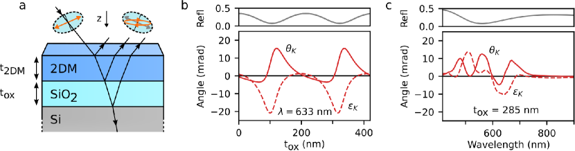
We model the thin layered systems as a series of stacked parallel homogeneous layers, where the first and last layer (being air and Si), are semi-infinite. An example of this geometry is illustrated in Fig. 1a, where a single 2D magnetic layer of thickness is on top of a SiO2/Si substrate with oxide thickness . The interfaces are assumed to be smooth, such that there are only specular reflections. Furthermore, we assume that the illumination intensity is low enough, such that the optical properties of the materials can be described by a linear dielectric permittivity tensor and magnetic permeability tensor . The intensity and polarization of the light that reflects off this stratified linear system are calculated using the transfer matrix method. We use a method similar to the one in, Yeh (1980) which is explained in full detail in the supplementary material.
The transfer matrix relates the components of the electric () and magnetic () field parallel to the layers, called and , at one interface of a medium to the other one. To construct a transfer matrix, we start by describing plane waves in a single layer. We begin from the Maxwell equations in isotropic homogeneous media, and consider plane waves with a frequency and wave vector , of the form , where is time and is the position in space. We can then derive the following wave equation:
| (1) |
Solving the above equation yields four values for the -component of , , and four corresponding polarization eigenmodes, , where labels the polarization mode. These solutions describe two plane waves traveling in the direction, and two in the direction. The transfer matrix is the diagonal matrix , which propagates the eigenmodes with wave vector components from one interface to the other one over a distance , after it is transformed from the basis of the eigenmode amplitudes to the the basis of the amplitudes of the and components. The transfer matrix of the whole system is simply the product of the transfer matrices of the individual layers, since and are continuous across the interfaces. This matrix is used to calculate the amplitudes of the eigenmodes of the reflected and transmitted light, and from this the reflected intensity and polarization.
We apply the above method to the system illustrated in Fig. 1a, where the 2D ferromagnet is monolayer CrI3 with a thickness of = 0.7 nm. The dielectric tensor of ferromagnetic monolayer CrI3 is taken from Wu et al.Wu et al. (2019), where it is calculated from first-principles methods taking excitonic effects into account. The dielectric constants of Si and thermally grown SiO2 are experimental values from Herzinger et al. Herzinger et al. (1998) The magnetic permeability of all materials is approximated by the scalar vacuum permeability . Using these parameters, we calculate the Kerr angle , Kerr ellipticity , and reflected intensity of linearly polarized light hitting the sample at normal incidence and polar configuration. The results are shown in Fig. 1b and 1c as a function of and wavelength respectively.
Fig 1b shows a clear periodic behavior of the MOKE signals as a function of , with a period of 216 nm, corresponding to half a wavelength in SiO2. It also shows that the Kerr angle and ellipticity attain their maximum values when the reflected intensity is close to a minimum, and vice-versa. In Fig. 1c, the largest MOKE signals are found in the wavelength range from 400 nm to 750 nm, where the wavelength dependence of and is caused primarily by the wavelength dependence of the dielectric tensor of CrI3. Again, and attain their maximum values when the reflectivity is close to a minimum. These results show that the oxide thickness and the wavelength of the light have a strong impact on the sign and magnitude of the MOKE signals. By optimizing or the wavelength, the signals can already change by as much as 20 mrad in this example, while still having a sizable reflectivity of more than 6%.
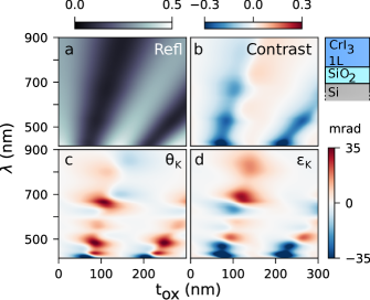
In order to get a complete picture of the impact of each parameter on the signals, we explore the full parameter space, varying both the wavelength and oxide thickness for a CrI3 monolayer on a SiO2/Si substrate (Fig. 2). Besides the reflectivity, , and , we also calculate the contrast for the CrI3 layer. This can be used to locate the target flake, usually a few m in size and therefore hard to find on a large substrate, using a microscope, or using a reflectivity scan in a laser based experiment. The contrast is defined as , where and are the reflected intensity of the system with and without CrI3 respectively. The reflectivity in Fig. 2 shows a clear fan pattern. The periodicity in in our simulated reflectivity corresponds to half a wavelength in the SiO2, which strongly suggests that this fan pattern is caused by the interference of the light reflected from the top and bottom interface of the SiO2, similar to graphene-based systems. Blake et al. (2007) The same pattern appears for , , and , indicating that the interference in the SiO2 layer also has a large effect on the contrast and MOKE signals. Additional features at 420 nm, 500 nm, and 680 nm, can also be seen, and originate from the wavelength dependence of the dielectric tensor of CrI3 (see supplementary material). By tuning both the wavelength and oxide thickness, and can be tuned over a range of several tens of milliradians while keeping the reflectivity above 5%. Furthermore, when the Kerr rotation and ellipticity are maximized, the contrast is large as well, making it easier to locate the CrI3 using e.g. a simple reflectivity scan.
The above results can be compared to the experimental results from Huang et al. Huang et al. (2017) In their experimental work, using a laser with a wavelength of 633 nm and = 285 nm, they obtained mrad. Our theoretical result of 3.5 mrad is within the experimental error margin. Our results are also in agreement with the absence of an experimental signal at a wavelength of 780 nm for this system. We find that the MOKE signals at these wavelengths are reduced by about a factor of ten and could easily be obscured by the experimental noise. Fig. 1 also indicates that the combination of an oxide thickness of 285 nm and a laser wavelength of 633 nm does not result in the largest Kerr rotation. Using instead an oxide thickness of 335 nm would increase by more than a factor of 4, or if the wavelength is changed to 560 nm, the Kerr rotation can increase by a factor of about 3.
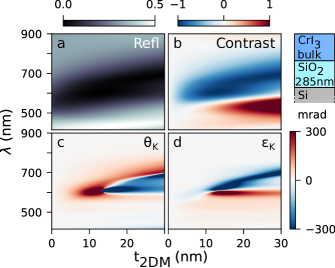
The 2DM thickness can also strongly affect the MOKE signals. Fig. 3 shows the dependence of the magneto-optical signals as a function of both wavelength and 2DM thickness, using the dielectric tensor of ferromagnetic bulk CrI3 taken from Wu et al.Wu et al. (2019) While the theoretical values of used in our calculations differ slightly from the available experimental values, Grant and Street (1968); Huang et al. (2017) our main findings are not altered if we consider the experimental values. We therefore opt for using the theoretical values since they span a larger wavelength range. For comparison, we provide calculations using the experimental values in the supplementary material. Interestingly, and have a non-monotonic behavior, showing a strong peak and dip around a wavelength of 600 nm CrI3 thickness of 14 nm. The extreme values of and approach and respectively. The reflectivity at these points is around 0.2% for the maximum Kerr rotation and 0.4% for the maximum Kerr ellipticity. These extreme MOKE signals can therefore be very hard to detect. However, and can still be changed over a range of a few hundred milliradians when tuning the wavelength and CrI3 thickness, while keeping the reflectivity above 5% and having a good contrast.
Due to the air sensitivity of many 2DMs, they are often encapsulated in hBN. Huang et al. (2018); Wang et al. (2018) The presence of the hBN layers also leads to thin-film interference effects and thus can be used to engineer the magneto-optical signals as well. Jin et al. (2020) To explore the impact of hBN encapsulation, we study the MOKE signals in monolayer CrI3 encapsulated by a top and bottom hBN flake with the same thickness . The refractive index of hBN needed for the simulation is calculated using the single oscillator model, , where = 164.4 nm and = 3.263 are determined experimentally by Lee et al. Lee et al. (2019) The simulation results for an oxide layer of 285 nm are shown in Fig. 4. We have also investigated the effect of the hBN thickness on the signal-to-noise ratio (see supplementary material). A striking result is that an hBN thickness of about ten nanometers, a typical thickness for hBN flakes used for encapsulation in experimental studies, can already lead to dramatic changes in the reflectivity, contrast, and Kerr signals. Therefore, one should take into account the system as a whole when engineering their heterostructures for optimal MOKE signals. The hBN encapsulation is particularly important, since the wavelength and oxide thickness are usually more difficult to vary, while hBN flakes of various thicknesses can be easily found in a single exfoliation run. Therefore, in addition to protecting the 2DM against degradation, hBN encapsulation can be used as an active method for magneto-optical signal enhancement.

The common feature in the results of the simulation of the three systems above that and are maximized when the reflectivity is close to a minimum, is a general and well-known phenomenon. Mansuripur, Connell, and Goodman (1982); Zak et al. (1990); Bass and Mahajan (2010) It can be explained by the behavior of the reflection coefficients for the electric field of the two circular polarizations, and , near the reflectivity minimum. In this region, the magnitude of both reflection coefficients are small, and their complex phases change rapidly with wavelength and layer thickness. The exact parameter values around which these coefficients have a minimum and change phase are different for and due to the circular birefingence and dichroism caused by the magnetic layer. Therefore, both the ellipticity, given by , and the Kerr rotation, given by , can become very large when the total reflectivity is near a minimum, as is explained in more detail in the supplementary material. On the other hand, if the reflectivity is large, both and are large, meaning that their relative difference is small, and that their complex phase changes slowly with wavelength and layer thickness. This will result in a low Kerr ellipticity and rotation respectively. Therefore, the extreme MOKE signals of e.g. and calculated for the CrI3(bulk)-SiO2(285nm)-Si stack can only occur at a low reflectivity. This reasoning is not restricted to the samples treated in this paper. A general method to increase the Kerr rotation and ellipticity of a multi-layer sample is to use a combination of wavelength and thickness of the layers that minimizes the reflectivity. A reduction of the reflectivity, and a corresponding increase the magneto-optical signals, can also be achieved by adding new layers to the sample. Such anti-reflection coatings have been used for over half a century to enhance Kerr signals from magnetic films. Kranz and Drechsel (1958); Mansuripur, Connell, and Goodman (1982); Cantwell et al. (2006); Kim et al. (2020)
Here we showed that thin-film interference can be a useful tool for improving magneto-optical signals in magnetic van der Waals systems. Through careful sample or heterostructure engineering, one is able to optimize their system for a particular experimental setup, improving the signal-to-noise ratio and measurement speed. The optimization of the signals can be done by choosing a particular illumination wavelength, substrate, thickness of the van der Waals magnet, or hBN used for encapsulation. The signal improvement, reaching several tens of miliradians, could lead to the identification of weaker signals from more delicate effects, such as chiral magnetic structures embedded in a homogeneously magnetized lattice.
Supplementary Material
See supplementary material for the simulation details, graphs of the dielectric tensors used in the simulations, simulation results for other 2D magnetic monolayers, and an explanation for why the Kerr rotation and ellipticity are large when the reflectivity is close to a minimum.
Acknowledgements.
We thank Alejandro Molina-Sánchez, for sharing their data on the dielectric tensor for chromium trihalides. This work was supported by the Zernike Institute for Advanced Materials, the Dutch Research Council (NWO Start-Up, STU.019.014), and the European Union’s Horizon 2020 research and innovation programme under grant agreement No 785219 (Graphene Flagship Core 3).Data availability
The data that support the findings of this study are available from the corresponding author upon reasonable request.
References
- Petit et al. (2008) D. Petit, A.-V. Jausovec, D. Read, and R. P. Cowburn, Journal of Applied Physics 103, 114307 (2008).
- Rogez et al. (2009) G. Rogez, B. Donnio, E. Terazzi, J.-L. Gallani, J.-P. Kappler, J.-P. Bucher, and M. Drillon, Advanced Materials 21, 4323 (2009).
- McCord (2015) J. McCord, Journal of Physics D: Applied Physics 48, 333001 (2015).
- Jiang et al. (2018) S. Jiang, L. Li, Z. Wang, K. F. Mak, and J. Shan, Nature Nanotechnology 13, 549 (2018).
- Gibertini et al. (2019) M. Gibertini, M. Koperski, A. F. Morpurgo, and K. S. Novoselov, Nature Nanotechnology 14, 408 (2019).
- Dickson et al. (2005) W. Dickson, S. Takahashi, R. Pollard, R. Atkinson, and A. V. Zayats, IEEE Transactions on Nanotechnology 4, 229 (2005).
- Savoini et al. (2011) M. Savoini, F. Ciccacci, L. Duò, and M. Finazzi, Review of Scientific Instruments 82, 023709 (2011).
- Lange et al. (2017) M. Lange, S. Guénon, F. Lever, R. Kleiner, and D. Koelle, Review of Scientific Instruments 88, 123705 (2017).
- Beaurepaire et al. (1996) E. Beaurepaire, J.-C. Merle, A. Daunois, and J.-Y. Bigot, Physical Review Letters 76, 4250 (1996).
- Kirilyuk, Kimel, and Rasing (2010) A. Kirilyuk, A. V. Kimel, and T. Rasing, Reviews of Modern Physics 82, 2731 (2010).
- Koopmans et al. (2010) B. Koopmans, G. Malinowski, F. Dalla Longa, D. Steiauf, M. Fähnle, T. Roth, M. Cinchetti, and M. Aeschlimann, Nature Materials 9, 259 (2010).
- Wu, Jiang, and Weng (2010) M. W. Wu, J. H. Jiang, and M. Q. Weng, Physics Reports 493, 61 (2010).
- Zhang et al. (2020) X.-X. Zhang, L. Li, D. Weber, J. Goldberger, K. F. Mak, and J. Shan, Nature Materials (2020).
- Huang et al. (2017) B. Huang, G. Clark, E. Navarro-Moratalla, D. R. Klein, R. Cheng, K. L. Seyler, Seyler, D. Zhong, E. Schmidgall, M. A. McGuire, D. H. Cobden, W. Yao, D. Xiao, P. Jarillo-Herrero, and X. Xu, Nature 546, 270 (2017).
- Gong et al. (2017) C. Gong, L. Li, Z. Li, H. Ji, A. Stern, Y. Xia, T. Cao, W. Bao, C. Wang, Y. Wang, Z. Q. Qiu, R. J. Cava, S. G. Louie, J. Xia, and X. Zhang, Nature 546, 265 (2017).
- Bonilla et al. (2018) M. Bonilla, S. Kolekar, Y. Ma, H. C. Diaz, V. Kalappattil, R. Das, T. Eggers, H. R. Gutierrez, M.-H. Phan, and M. Batzill, Nature Nanotechnology 13, 289 (2018).
- Fei et al. (2018) Z. Fei, B. Huang, P. Malinowski, W. Wang, T. Song, J. Sanchez, W. Yao, D. Xiao, X. Zhu, A. F. May, W. Wu, D. H. Cobden, J.-H. Chu, and X. Xu, Nature Materials 17, 778 (2018).
- Novoselov et al. (2004) K. S. Novoselov, A. K. Geim, S. V. Morozov, D. Jiang, Y. Zhang, S. V. Dubonos, I. V. Grigorieva, and A. A. Firsov, Science 306, 666 (2004).
- Abergel, Russell, and Fal’Ko (2007) D. S. L. Abergel, A. Russell, and V. I. Fal’Ko, Applied Physics Letters 91, 063125 (2007).
- Blake et al. (2007) P. Blake, E. W. Hill, A. H. Castro Neto, K. S. Novoselov, D. Jiang, R. Yang, T. J. Booth, and A. K. Geim, Applied Physics Letters 91, 063124 (2007).
- Castellanos-Gomez, Agraït, and Rubio-Bollinger (2010) A. Castellanos-Gomez, N. Agraït, and G. Rubio-Bollinger, Applied Physics Letters 96, 213116 (2010).
- Late et al. (2012) D. J. Late, B. Liu, H. S. S. R. Matte, C. N. R. Rao, and V. P. Dravid, Advanced Functional Materials 22, 1894 (2012).
- Castellanos-Gomez et al. (2013) A. Castellanos-Gomez, E. Navarro-Moratalla, G. Mokry, J. Quereda, E. Pinilla-Cienfuegos, N. Agraït, H. S. J. van der Zant, E. Coronado, G. A. Steele, and G. Rubio-Bollinger, Nano Research 6, 191 (2013).
- Li et al. (2013) H. Li, J. Wu, X. Huang, G. Lu, J. Yang, X. Lu, Q. Xiong, and H. Zhang, ACS Nano 7, 10344 (2013).
- Berreman (1972) D. W. Berreman, Journal of the Optical Society of America 62, 502 (1972).
- Yeh (1980) P. Yeh, Surface Science 96, 41 (1980).
- Mansuripur, Connell, and Goodman (1982) M. Mansuripur, G. A. N. Connell, and J. W. Goodman, Journal of Applied Physics 53, 4485 (1982).
- Zak et al. (1990) J. Zak, E. R. Moog, C. Liu, and S. D. Bader, Journal of Magnetism and Magnetic Materials 89, 107 (1990).
- Cantwell et al. (2006) P. R. Cantwell, U. J. Gibson, D. A. Allwood, and H. A. M. MacLeod, Journal of Applied Physics 100, 093910 (2006).
- Sumi, Awano, and Hayashi (2018) S. Sumi, H. Awano, and M. Hayashi, Scientific Reports 8, 776 (2018).
- Bräuer et al. (2009) B. Bräuer, M. Fronk, D. Lehmann, D. R. Zahn, and G. Salvan, Journal of Physical Chemistry B 113, 14957 (2009).
- Humlíček (2005) J. Humlíček, in Handbook of Ellipsometry, edited by H. G. Tompkins and E. A. Irene (William Andrew Publishing, Norwich, NY, 2005) pp. 3 – 91.
- Schubert (2005) M. Schubert, in Handbook of Ellipsometry, edited by H. G. Tompkins and E. A. Irene (William Andrew Publishing, Norwich, NY, 2005) pp. 637 – 717.
- Fujiwara (2007) H. Fujiwara, Spectroscopic Ellipsometry (John Wiley & Sons, Ltd, 2007).
- Huang et al. (2018) B. Huang, G. Clark, D. R. Klein, D. MacNeill, E. Navarro-Moratalla, K. L. Seyler, N. Wilson, M. A. McGuire, D. H. Cobden, D. Xiao, W. Yao, P. Jarillo-Herrero, and X. Xu, Nature Nanotechnology 13, 544 (2018).
- Wang et al. (2018) Z. Wang, T. Zhang, M. Ding, B. Dong, Y. Li, M. Chen, X. Li, J. Huang, H. Wang, X. Zhao, Y. Li, D. Li, C. Jia, L. Sun, H. Guo, Y. Ye, D. Sun, Y. Chen, T. Yang, J. Zhang, S. Ono, Z. Han, and Z. Zhang, Nature Nanotechnology 13, 554 (2018).
- Fang et al. (2018) Y. Fang, S. Wu, Z.-Z. Zhu, and G.-Y. Guo, Physical Review B 98, 125416 (2018).
- Ma et al. (2019) Z. Ma, W. Zhu, G. Lin, Y. Liu, F. Jin, Y. Yang, T. Wu, X. Luo, Y. Sun, J. Chen, Y. Sun, C. Zhou, and Z. Sheng, AIP Advances 9, 125116 (2019).
- Wu et al. (2019) M. Wu, Z. Li, T. Cao, and S. G. Louie, Nature Communications 10, 2371 (2019).
- Jin et al. (2020) C. Jin, Z. Tao, K. Kang, K. Watanabe, T. Taniguchi, K. F. Mak, and J. Shan, Nature Materials 19, 1290 (2020).
- Molina-Sánchez et al. (2020) A. Molina-Sánchez, G. Catarina, D. Sangalli, and J. Fernández-Rossier, Journal of Materials Chemistry C 8, 8856 (2020).
- Herzinger et al. (1998) C. M. Herzinger, B. Johs, W. A. McGahan, J. A. Woollam, and W. Paulson, Journal of Applied Physics 83, 3323 (1998).
- Grant and Street (1968) P. M. Grant and G. B. Street, Bulletin of the American Physical Society 13, 415 (1968).
- Lee et al. (2019) S.-Y. Lee, T.-Y. Jeong, S. Jung, and K.-J. Yee, Physica Status Solidi B 256, 1800417 (2019).
- Bass and Mahajan (2010) M. Bass and V. N. Mahajan, Handbook of optics, 3rd ed., Vol. I (McGraw-Hill, 2010).
- Kranz and Drechsel (1958) J. Kranz and W. Drechsel, Zeitschrift für Physik 150, 632 (1958).
- Kim et al. (2020) D. Kim, Y.-W. Oh, J. U. Kim, S. Lee, A. Baucour, J. Shin, K.-J. Kim, B.-G. Park, and M.-K. Seo, Nature Communications 11, 5937 (2020).