Best CNTFET Ternary Adders?
Abstract
The MUX implementation of ternary half adders and full adders using predecessor and successor functions lead to the most efficient efficient implementation using the smallest transistor count. These designs are compared with the binary implementation of the corresponding half adders and full adders using the MUX technique or the typical complementary CMOS circuit style. The transistor count ratio between ternary and binary implementations is always greater than the information ratio ( = 1.585) between ternary and binary wires.
I Introduction
Many ternary half adders and full adders have been presented in the last decade. The most significant papers are [1], [2], [3], [4]. [5], [6], [7]. In [8], we have compared different implementations of quaternary adders. The best quaternary one has been presented in [9]. It is based on the use of multiplexers. In this paper, we show that this approach also leads to the best implementation of ternary half and full adders. The design is based on CNTFET technology. This technology is far from being a mature technology. As of 2020, FinFET technology integrates millions of times more transistors than CNTFET technology. However, CNTFET has a big advantage for designing multivalued circuits. While it basically uses the typical CMOS circuit styles, the threshold levels of the different multivalued gates can be got by adjusting the diameter of each used transistor. This technology is used in this paper. We first present the MUX based design of the ternary half adder. Then we present the full adder design. These implementation are compared with the similar MUX based implementation and the conventional implementation of the binary versions.
II Ternary Half Adders
Table I presents the truth table of the ternary half-adder.
Ternary half adders and full adders have ternary inputs and outputs and binary carry inputs and outputs.
-
•
Ternary values (0,1,2) corresponding to 0, and voltage levels
-
•
According to the circuit style that is used, the binary values may have levels 0 and or 0 and .
The technique used in [9] is based on multiplexers. In this approach, the carry signals are used as control inputs of MUX: they are never used as input values of these MUX. The binary levels are thus 0 and . The corresponding binary values are 0 and 2.
| SUM | CARRY | ||||||
|---|---|---|---|---|---|---|---|
| X/Y | 0 | 1 | 2 | 0 | 1 | 2 | |
| 0 | 0 | 1 | 2 | 0 | 0 | 0 | |
| 1 | 1 | 2 | 0 | 0 | 0 | 1 | |
| 2 | 2 | 0 | 1 | 0 | 1 | 1 | |
Computation of the Half Adder SUM is processed by the following rules:
-
•
When X = 0, SUM = Y
-
•
When X = 1, SUM = (Y+1) mod (3). The corresponding circuit is called successor circuit.
-
•
When X = 2, SUM = (Y-1) mod (3). The corresponding circuit is called predecessor circuit.
-
•
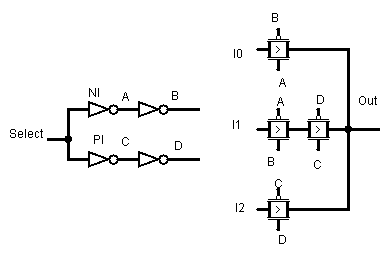
According to X, a ternary MUX provides the correct SUM output.
Threshold detectors circuits are implemented by the inverters NI and PI, according to Table 2. These inverters are generally called NTI and PTI, but this is confusing as they are binary inverters: the outputs are binary ones and they only have one threshold level. The only difference with typical binary inverters is the specific threshold levels. Assuming, and 0 ternary levels, the threshold levels are and when the threshold level of a binary inverter is . The NI and PI threshold levels are obtained by choosing the appropriate diameter for the different CNTFET transistors. They are shown in left part of Figure 1. The implementation of the ternary MUX is shown in right part of Figure 1.
| NI | PI | |
|---|---|---|
| 0 | 2 | 2 |
| 1 | 0 | 2 |
| 2 | 0 | 0 |
Figure 2 presents the Successor and Predecessor circuits with two power supplies ( and . A, B, C, D outputs of NI and PI inverters control the different transistors: for each ternary input X, only one path is active between or or ground and the corresponding output. The drawback of this approach is the supplementary power supply. Figure 3 presents the successor and predecessor circuits with only one power supply . The intermediate level is got through a voltage divider by using resistor-like transistors. The drawback of this approach is a static power dissipation when the output is 1.
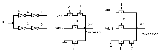
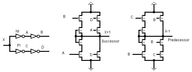
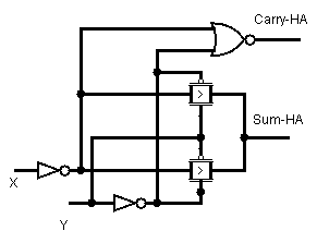
Figure 4 presents the ternary half-adder circuit. The carry output is:
-
•
When X = 0, = 0
-
•
When X = 1, = 1 if Y = 2 () according to Table 2)
-
•
When X = 2, = 1 if () according to Table 2)
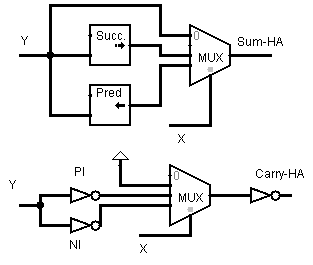
Table III presents the transistor count for the half adders.
| 2 PS | 1 PS | |
|---|---|---|
| Succ-Pred | 8 | 14 |
| MUX | 16 | 16 |
| PI-NI | 16 | 16 |
| NOT | 2 | 2 |
| TOTAL | 42 | 48 |
Table IV presents the transistor count for different ternary half adders proposed in the last ten years.
III Ternary Full Adders
When = 0, the full adder truth table was presented in Table 1 (half-adder).When = 1, the truth table is given in Table V.
| SUM | CARRY | ||||||
|---|---|---|---|---|---|---|---|
| X/Y | 0 | 1 | 2 | 0 | 1 | 2 | |
| 0 | 1 | 2 | 0 | 0 | 0 | 1 | |
| 1 | 2 | 0 | 1 | 0 | 1 | 1 | |
| 2 | 0 | 1 | 2 | 1 | 1 | 1 | |
Still using the MUX approach, the SUM output of the full adder is given by
-
•
If = 0, then else
Another approach directly computes as a function of and X.
-
•
When X = 0: if = 0 then SUM = Y else SUM = (Y+1) mod (3).
-
•
When X = 1, if = 0 then SUM = (Y+1) mod (3) else SUM = (Y-1) mod (3).
-
•
When X = 2, if = 0 then SUM= (Y-1) mod (3) else SUM =Y.
is the carry output when = 1:
-
•
When X = 0, = 1 if Y = 2 ( according to Table 2)
-
•
When X = 1, = 1 if ( according to Table 2)
-
•
When X = 2, = 1
If = 0 then = else =
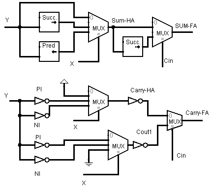
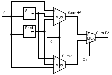
Figure 5 and Figure 6 use two new different types of MUXes:
-
•
MUXes with ternary inputs and binary control;
-
•
MUXes with binary inputs and binary control.
Both types use the same typical MUX2 binary circuit (Figure 7)
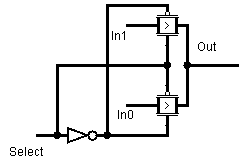
Table VI presents the transistor counts for the two versions of the ternary full adder with two power supplies. Table VII provides the same information for one power supply.
| Carry | SUM V1 | SUM V2 | FA-V1 | FA-V2 | |
|---|---|---|---|---|---|
| SUCC- PRED | 0 | 12 | 8 | ||
| MUX3 | 16 | 8 | 16 | ||
| MUX2 | 4 | 4 | 4 | ||
| PI-NI | 0 | 24 | 16 | ||
| NOT | 6 | 2 | 2 | ||
| TOTAL | 26 | 50 | 46 | 76 | 72 |
| Carry | SUM V1 | SUM V2 | FA-V1 | FA-V2 | |
|---|---|---|---|---|---|
| SUCC- PRED | 0 | 21 | 14 | ||
| MUX3 | 16 | 8 | 16 | ||
| MUX2 | 4 | 4 | 4 | ||
| PI-NI | 0 | 24 | 16 | ||
| NOT | 6 | 2 | 2 | ||
| TOTAL | 26 | 59 | 52 | 83 | 78 |
Table VIII presents the transistor count for different ternary full adders proposed in the last decade.
IV Comparing with binary adders
IV-A Binary Half Adder
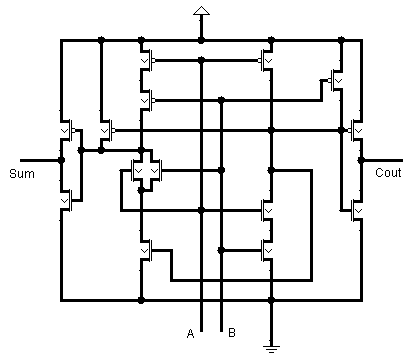
Using the same MUX technique, the binary half-adder is shown in Figure 8. It uses 12 T. Permuting the MUX inputs and adding an output inverter would lead to 14 T with restored output levels. The transistor count is then the same as a typical conventional approach used in standard cell libraries [10], as shown in Figure 9 .
IV-B Binary Full Adder
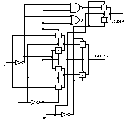
With the MUX approach, the binary full adder is presented in Figure 10. It corresponds to the following rules:
-
•
If = 0 then = X XOR Y else X NXOR Y. XOR and NXOR functions are implemented using MUXes.
-
•
If = 0 then = X.Y else = X+Y.
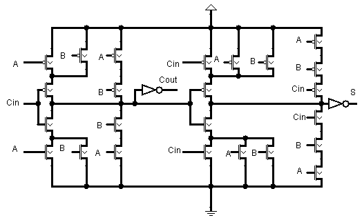
The MUX based full adder has 30 T. A version with restored output levels would have 34 T. It could be outlined that the MUX approach has more transistors than the typical conventional full adder with complementary CMOS shown in Figure 11. Many proposals using less than 28 T have been proposed in the literature.
V Conclusion
The proposed ternary half adders and full adders have less transistors than all the previously proposed ones. It seems that the MUX approach with successor and predecessor circuits is the best one to implement ternary arithmetic circuits. It looks like the transistor counts are close to the minimal possible value. The only valid comparison between ternary and binary circuit is based on the information ratio. According to Shannon theory of information, when N events have the same probability to occur, the corresponding amount of information is bits (or Shannon). When N = 2, I = 1 bit. When N = 3, I = 1.585 bits. A ternary wire carries 1.585 times the amount of information of a binary one. This 1.585 information ratio must be used to compare binary and ternary circuits. For instance, an 8-bit binary adder can be compared to a 5-trit ternary adder as they process approximately the same amount of information. 8/5 is close to 1.585. The difference results from rounding issues. Considering the most conservative implementation of binary circuits, the transistor count ratio between ternary and binary half adder is 42/14 = 3 and 72/28 = 2.57 for the full adder when using two power supplies for the ternary case. With only one power supply, the ratios are respectively 48/14 = 3.4 and 78/28 = 2.8. Both ratios are greater than 1.585. It means that the best ternary implementation leads to more transistors, more chip area, more interconnects and more power dissipation than the corresponding conservative binary ones. These results are not surprising. 3 is not the best base for computation [11] and multivalued circuits are restricted to a small niche [12].
References
- [1] S. Lin, Y-B. Yin and F. Lombardi, “CNTFET-Based Design of Ternary Logic Gates and Arithmetic Circuit", IEEE Transactions on Nanotechnology, Vol 10, No 2, March 2011.
- [2] H. Samadi, A. Shahhoseini and F. Aghaei-liavali, “A new method on designing and simulating CNTFET-based ternary gates and arithmetic circuits", Microelectron. J, vol 63, pp 41-48, May 2017, doi: 10.1016/j.mejo.2017.02.018
- [3] S. K. Sahoo, G. Akhilesh, R. Sahoo and M. Muglikar, “High-Performance Ternary Adder Using CNTFET," in IEEE Transactions on Nanotechnology, vol. 16, no. 3, pp. 368-374, May 2017, doi: 10.1109/TNANO.2017.2649548.
- [4] R.A. Jaber, A.Kassem, A.M. El-Hajj, L.A. El-Nimri and A.Massoud Haidar, “High-Performance and Energy-Efficient CNTFET-Base Designs for Ternary Logic Circuits", IEEE Access, Vol 7, pp. 93871-93886, 2019.
- [5] R. F. Mirzaee, K. Navi and N. Bagherzadeh, “High-Efficient Circuits for Ternary Addition", Hindawi Publishing Corporation, VLSI Design, Volume 2014, Article ID 534587, 15 pages http://dx.doi.org/10.1155/2014/534587
- [6] S. A. Ebrahimi, P. Keshavarzian, S. Sorouri, and M. Shahsavari, “Low power CNTFET-based ternary full adder cell for nanoelectronics", International Journal of Soft Computing and Engineering, vol. 2, pp. 291-295, 2012.
- [7] P. Keshavarzian and R. Sarikhani, “A novel CNTFET-based ternary full adder", Circuits, Systems, and Signal Processing, vol. 33, no.3, pp. 665-679, 2014.
- [8] D. Etiemble, “Comparing quaternary and binary multipliers", arXiv:1908.07299 [cs.AR]
- [9] E. Roosta and S. A. Hosseiny, "A Novel Multiplexer-Based Quaternary Full Adder in Nanoelectronics", Circuits, Systems and Signal Processing, https://doi.org/10.1007/s00034-019-01039-8
- [10] VLSI Technology Standard Cell Library, January 2008 http://www.vlsitechnology.org/html/cells/wsclib013/ha2.html
- [11] D. Etiemble, “Ternary circuits: why R = 3 is not the Optimal Radix for Computation", August 2019, arXiv:1908.06841 [cs.AR],
- [12] D. Etiemble, “Why M-Valued Circuits are restricted to a Small Niche”, in Journal of Multiple Valued Logic and Soft Computing, Vol. 9 , No1, 2003.