High-Level FPGA Accelerator Design for
Structured-Mesh-Based Explicit
Numerical Solvers
Abstract
This paper presents a workflow for synthesizing near-optimal FPGA implementations for structured-mesh based stencil applications for explicit solvers. It leverages key characteristics of the application class, its computation-communication pattern, and the architectural capabilities of the FPGA to accelerate solvers from the high-performance computing domain. Key new features of the workflow are (1) the unification of standard state-of-the-art techniques with a number of high-gain optimizations such as batching and spatial blocking/tiling, motivated by increasing throughput for real-world work loads and (2) the development and use of a predictive analytic model for exploring the design space, resource estimates and performance. Three representative applications are implemented using the design workflow on a Xilinx Alveo U280 FPGA, demonstrating near-optimal performance and over 85% predictive model accuracy. These are compared with equivalent highly-optimized implementations of the same applications on modern HPC-grade GPUs (Nvidia V100) analyzing time to solution, bandwidth and energy consumption. Performance results indicate equivalent runtime performance of the FPGA implementations to the V100 GPU, with over 2 energy savings, for the largest non-trivial application synthesized on the FPGA compared to the best performing GPU-based solution. Our investigation shows the considerable challenges in gaining high performance on current generation FPGAs compared to traditional architectures. We discuss determinants for a given stencil code to be amenable to FPGA implementation, providing insights into the feasibility and profitability of a design and its resulting performance.
Index Terms:
FPGAs, Stencil Applications, Explicit solversI Introduction
Field Programmable Gate Arrays (FPGAs) have become highly attractive as accelerator architectures by virtue of their high performance, low power consumption, and re-programmability. As a result, FPGAs have gained a foothold in a wider range of application domains such as cyber security [1], databases [2], and deep learning [3]. In recent years, the integration of FPGAs as first-class accelerator platforms has also attracted significant interest in the high-performance (HPC) and scientific computing community, particularly in the financial computing domain [4]. They have also emerged as potential accelerator platforms for cloud computing [5]. However, a key limitation has been the design effort needed to produce performant accelerators for FPGAs, requiring hardware expertise and an alternative approach to programming that is more data-flow oriented. Commercial FPGA vendors have attempted to address this problem with high level synthesis (HLS) tools that can translate programs written in standard high-level languages such as C/C++ or OpenCL. However, these tools still require low level modification of code to produce accelerators with optimum performance.
One solution to this problem is to leverage key characteristics of an application, its computation-communication patterns or motifs to explore the design space on hardware. Once the best optimization strategy for a given motif is identified for the target hardware, it can be used as a design template for similar applications, even going so far as to create higher-level frameworks such as DSLs that can automatically generate the accelerator implementations. Such a strategy has become an important technique in developing performance portable massively parallel HPC applications given the increasing diversity of processor architectures [6, 7, 8, 9].
In this paper we apply such an analysis to the domain of structured-mesh-based explicit numerical solvers, characterized by stencil computations, targeting FPGAs. These codes frequently appear as the core motif in solvers for partial differential equation (PDEs). As such, they are used in applications from a wide range of fields, including computational fluid dynamics (CFD), hydro-dynamics, financial computing, and oil/gas exploration simulations. The key characteristic is the loop over a “rectangular” multi-dimensional set of mesh points using one or more “stencils” to access data. This is in contrast to unstructured meshes that require explicit connectivity information [7] between neighboring mesh elements via mappings.
Considerable previous research has developed a range of strategies to synthesize optimized FPGA implementations for stencil codes [10, 11, 12, 13, 14, 15, 16, 17, 18, 19, 20]. Most recent works utilize HLS tools, usually compiling OpenCL, and target both 2D and 3D stencil applications. They develop a number of standard techniques, ranging from basic methods such as cell-parallel/vectorization, unrolling the iterative loop, to more complex transformations such as spatial/temporal blocking (tiling), in order to best utilize FPGA resources for maximum performance. However, many of these previous works target optimizations specific to an application in isolation without developing a design strategy that can be applied to other stencil codes. While some [12, 16] does attempt to generalize accelerator implementations for stencil codes, they only target simpler stencil applications without exploiting higher-gain optimizations. A key gap is the lack of a unifying design strategy particularly focusing on realistic applications.
As such, an open question remains regarding how to optimize implementation of stencil applications on FPGAs, and how characteristics of the application and various optimizations determine performance compared to traditional CPU and GPU architectures. To this end, in this paper we present an initial proposal and unifying workflow for designing near-optimal FPGA implementations for structured-mesh based stencil applications together with analytical models that enable exploration of the design space for stencil accelerators on modern FPGAs. Specifically, we make the following contributions:
-
•
We propose an implementation template, and an accompanying step-wise optimization strategy for conversion of structured-mesh, explicit, iterative stencil applications to FPGA accelerators. Given the hardware resource constraints, we focus on features of the application that are amenable for FPGA implementation and optimizations for gaining near-optimal performance. A key optimization, novel in this area, is the batched execution of multiple independent stencil problems on an FPGA.
-
•
Targeting current generation Xilinx FPGAs, we present the design and optimization of three contrasting, representative explicit stencil solvers, comparing a range of alternatives based on resource and performance trade-offs. The applications include both 2D and 3D stencil solvers and multiple stencil loops.
-
•
We develop a predictive analytic model that provides estimates for determining the feasibility of implementing a given stencil application on an FPGA using the proposed design strategy. The model calculates the resource requirements considering the optimizations implemented, together with memory requirements and limitations on operating frequency. It predicts the runtime of the resulting FPGA synthesis of the application accurate to within 15% of the achieved runtime.
-
•
Finally, the runtime, bandwidth and power/energy performance of the FPGA implementations developed with the proposed strategy are compared with highly optimized implementations on a traditional accelerator architecture, a modern Nvidia GPU.
Initial results on current generation Xilinx hardware demonstrate competitive performance compared to the best performance achieved for the same applications on traditional (in this case GPU) architectures using single precision floating-point (SP) representations. To our knowledge, such an extended workflow for stencil application development accompanied with a predictive model have not been previously presented. We believe that the proposed approach provides a promising strategy for use in industrial workloads from areas such as financial computing, standardizing the development cycle for these platforms.
The rest of the paper is organized as follows: Section II begins with a background on structured-mesh stencil applications together with previous work that explored FPGA implementations for this class of applications. Section III presents our proposed design strategy for implementing iterative stencil codes for FPGAs, as a step-by-step methodology, starting from the basic stencil loops, down to target FPGA code for the Xilinx Alveo U280 accelerator board. Further optimizations for the target synthesis is discussed in Section IV. The design including the advanced optimizations is then explored through the development of an analytic performance model. A performance analysis and benchmarking of the FPGA implementations compared against the performance of state-of-the-art optimized CPU and GPU implementations is presented in Section V. Finally, conclusions are presented in Section VI.
II Background
The key characteristic of structured-mesh stencil computations is loops over a “rectangular” multi-dimensional set of mesh points using one or more fixed data access patterns, called stencils, to access data. The main motivating numerical method here is the solution to Partial Differential Equations (PDEs), specifically based on the finite difference method. These techniques are used extensively in computational fluid dynamics (CFD), computational electro magnetics (CEM) in the form of iterative solvers. For example the finite difference scheme for the solution of a generic PDE can be given by the 2D explicit equation (1):
| (1) |
Here, U is a 2D mesh and a, b, c, d, and e are coefficients. In this example U is accessed at spatial mesh points (x-1,y), (x+1,y), (x,y-1), (x,y+1), and (x,y) which forms a five point stencil. In an explicit scheme the computation iterates over the full rectangular mesh, updating the solution at each mesh point, for the current time step, t+1, using the solution from the previous time step, t. The time step iteration usually continues until a steady state solution is achieved. There is a data dependency for the computations among multiple time step iterations, but no dependency within the spatial iterations. As such, each mesh point calculation within a time iteration can be computed in parallel. In contrast, an implicit scheme would update the solution at the current time step using values from the same time step, further introducing a data dependency within the spatial iterations. This leads to a much faster convergence to the final solution, but enforces an order in which a computation iterates over the mesh leading to limited parallelism. While both explicit and implicit schemes are equally used in production settings in scientific computing applications, we focus on explicit iterative solvers in this paper given their simplicity and higher parallelism.
II-A Related Work
Many previous works have targeted FPGAs for stencil computations. Early works [21, 22, 23] used Hardware Description Languages (HDL) for describing the architectures. However the process required extensive hardware knowledge and a time consuming development cycle. The introduction of High-Level Synthesis (HLS) tools has significantly improved developer productivity and time to design. As such more recent work [12, 16, 11, 13, 17] have all utilized HLS tools for implementing FPGA designs for stencil computations. As FPGAs have advanced to incorporate a variety of high bandwidth interfaces and memory types, the system level view of an accelerator architecture has become more important to achieving overall high performance.
The most comprehensive implementation workflow and optimization methodology to date is by Waidyasooriya et. al in [12, 16]. The authors use OpenCL and propose an optimization strategy for stencil applications targeting Intel FPGAs. A number of 2-D and 3-D stencil applications are developed through the above strategy, demonstrating up to 950 GFLOPS of achieved computational performance on Intel FPGAs. Runtime and bandwidth performance are compared to conventional GPU and multi-core CPU implementations. The work, however, limits the investigation to applications with only a single stencil loop over the mesh. Multiple stencil loops within a single time-step iterative loop are not considered.
A previous implementation of the 3D Reverse Time Migration (RTM) application, which has similarities to the RTM application we develop later in this paper, can be found in [10]. The implementation uses early-generation Xilinx FPGAs, prior to the introduction of HLS tools, but with designs equivalent to the techniques we use in this paper. The work in [14] uses Intel FPGAs with a design goal to enable unrestricted input sizes for stencil computations without sacrificing performance. They combine spatial and temporal blocking to avoid input size restrictions, and employ multiple FPGA-specific optimizations to tackle the added design complexity. The same authors apply these techniques to higher-order stencils in [15]. The use of spatial and temporal blocking is novel, which our work in this paper also addresses, but we extend it to variable sized tiling and multi-port implementations, generalizing the technique and incorporating it to our overall design workflow.
A number of previous works have also utilized high-level frameworks for generating efficient FPGA accelerators. The SDSLc framework [11] presents the use of source-to-source translation for generating parallel executables for a range of hardware platforms. These include CPUs, GPUs and FPGAs. The paper details optimizations such as iterative loop unrolling and full data reuse within FPGAs. Similarly the SODA framework [13] performs several optimizations including perfect data reuse by minimal reuse buffers and data quantization. Additionally it models the performance and predicts resource consumption, significantly reducing design time. The authors present competitive performance with multi-core CPU implementations and state-of-the-art stencil implementations on FPGAs. The main limitations of the work are fixed tile size and host based tiling. Due to the DSL’s support of only declarative programming, it is not clear whether any limitations exists for porting of complex kernels using SODA.
The more recent HeteroCL framework [17] addresses image processing applications. It also supports stencil applications through a SODA back-end. The HeteroCL DSL separates algorithm from compute, schedules and determines data types, and automatically translates SODA DSL to reflect the iteration factor, unroll factor and other parameters such as data width. A deep single kernel pipeline generated using the above frameworks usually suffers from routing congestion in modern large FPGAs from Xilinx that incorporate multiple Super Logic Regions (SLRs). In [18], Dohi et. al, use the proprietary MaxCompiler and MaxGenFD high-level design tools to implement finite-difference equations. The work is limited to Maxeler Technologies FPGA platforms and does not compare results with other FPGAs, GPUs or CPUs. The authors of [19] use the polyhedral model and implement a related framework to automatically accelerate iterative stencil loops on a multi-FPGA system. In contrast [20] develop a Scalable Streaming Array to implement stencil computations on multiple FPGAs, using a DSL, achieving reduced development time and near-peak performance. Automatic code generation is also used in [24] and has similarities to our design in this paper. However, it mainly focuses on non-iterative applications with multiple kernels, hence spanning designs over multiple FPGAs. Batching and tiling optimizations are not attempted.
In contrast to the above work, this paper presents a unifying strategy for the development of FPGA implementations of both 2-D and 3-D stencil applications, including multi-dimensional mesh elements and multiple stencil loops. We incorporate many of the optimization techniques in previous works that have usually been applied in isolation or on a single application. Additionally we introduce a number of further optimizations such as batching to achieve higher throughput in real-world/production workloads and settings. We also present a predictive analytic model that estimates the feasibility of implementing a given stencil application on a given FPGA platform. We compare the performance of the FPGA accelerators to equivalent highly-optimized implementations of the same applications on modern HPC-grade GPUs analyzing time to solution, bandwidth, and energy consumption. To our knowledge, the 3D RTM application developed in this work, using HLS tools for the FPGA using our design flow, motivated by real-world stencil codes, is also novel, being one of the few non-trivial applications presented in literature. Our investigation uncovers the determinants for a given stencil code to benefit from a FPGA implementation, providing insights into the feasibility of a design and its resulting performance.
III Accelerator Design
FPGAs differs from traditional CPUs and GPUs as they do not present a fixed general purpose architecture to be exploited using software. A program, made up of a sequence of instructions, is executed on a fixed CPU or GPU architecture that does not change. In contrast, an FPGA must be configured with an architecture that implements the data flow computation for a specific task. This leads to significantly reduced energy consumption compared to the CPUs and GPUs, primarily due to the locality of data movement within the mapped architecture rather than via multiple reads and writes to various stages of the memory hierarchy. The reconfigurability of FPGAs offers a significant advantage over the design of custom Application Specific Integrated Circuits (ASICs) which is much more time-consuming and costly and leads to a fixed architecture that cannot be modified post-design. FPGAs comprise a variety of basic circuit elements, including ample look-up-tables (LUTs) and registers, large numbers of digital signal processing (DSP) blocks on modern devices, block memories (BRAM/URAM), clock modules, and a rich routing fabric to connect these elements into a large logical accelerator architecture. While these resources are primarily suited to implementation of fixed point integer data-paths, they can be used to implement floating point data paths too, though these typically consume significantly more resources for the same computation. In modern Xilinx FPGAs, the overall die is split into a number of regions called Super Logic Regions (SLR) [25]. Bandwidth within an SLR is extremely high (TB/s) due to the wealth of connections and memory elements, while between SLRs it is limited by the number of silicon connections available. The BRAMs and URAMs that reside in SLRs provide high-speed, small blocks of on-chip memory, typically 10s of MB in total, recent devices like the U280 have close coupled High Bandwidth Memory (HBM) (8 GB on the U280) connected to multiple SLRs. HLS tools can typically connect multiple on-chip BRAMs or URAMs to obtain a larger block of memory. An FPGA board will also include much larger, but slower DDR4 (32 GB on the U280) memory as external memory. Managing the movement of data between these different types of memory is key to achieving high computational performance. The performance of an FPGA architecture is hard to predict, as it is impacted by various design characteristics beyond the level of parallelization applied. As a design grows and begins to occupy a larger portion of the FPGA, routing (i.e. connecting all the circuit elements together) becomes more challenging, and can reduce the achievable clock frequency and hence overall performance.
To achieve high computational throughput on FPGAs, a custom architecture is designed that is then implemented using the low-level circuit elements described above. A data-flow arrangement seeks to map a complex computation to a series of data-paths that implement the required computational steps with movement of data managed by direct connections. Compared to fixed CPU and GPU architectures where the steps in an algorithm are computed sequentially with intermediate results stored to registers, FPGA compute pipelines can be much deeper and more irregular parallelism can be exploited. Performing a stencil computation will then involve, starting up the pipeline (requiring some clock cycles equal to the pipeline depth) and outputting the result from the computation for each mesh point per clock cycle as a pipelined execution.
For CPU/GPU architectures such a computation is implemented using nested loops, iterating over the mesh and over the neighborhood points. On FPGAs these multiple levels of loops can be unrolled. Retaining an outer loop can be costly due to the need to flush the unrolled inner loop pipeline which can be long. Hence, multi-dimensional nested loops should be flattened to a 1D loop either manually or by using HLS directives such as loop_flatten. We have observed that manual flattening still provides the best performance and optimized resource utilization, as current Xilinx HLS compilers can make pessimistic scheduling decisions.
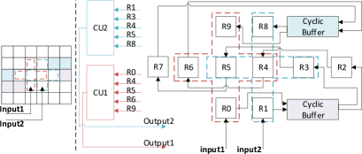
A key approach to gaining the best performance from the above computational pipeline is streaming data from/to external and near-chip memories to/from on-chip BRAMs/URAMs to feed the computational pipelines efficiently. A perfect data reuse path can be created by (1) using a First-In-First-Out (FIFO) buffer to fetch data from DDR4/HBM memory without interruption (allowing burst transfers) to on-chip memory, and then (2) by caching mesh points using the multiple levels of memory, from registers to BRAM/URAM. Fig. 1 illustrates such a data path for a 2D, 2nd order stencil. This technique has previously been referred to as window buffers [10]. A 2D, order stencil requires rows to be buffered to achieve perfect data reuse. Similarly, planes should be buffered for a 3D stencil. The total number of mesh elements needed to be buffered is the maximum number of mesh elements between any two stencil points. BRAM/URAMs can be used to design window buffers by using cyclic buffering. Given their high capacity, URAMs are preferred if the number of elements to be buffered is large.
Multiple pipelines for the same computation (i.e. loop body or kernel) can be created using HLS directives. This technique, called the cell-parallel method in [12] allows computation of the stencil on multiple mesh points simultaneously, provided that there are no data dependencies, which is the case for explicit schemes. The cell-parallel method is similar to SIMD vectorization on CPUs and SIMT on GPUs but on an FPGA it essentially creates parallel replicas of the computational units as opposed to single vector operations. However the resource availability in an FPGA limits the number of parallel units that can be synthesized on a given device. Fig. 1 illustrates a factor of 2 implementation, where the vectorization factor represents the number of mesh points updated in parallel.
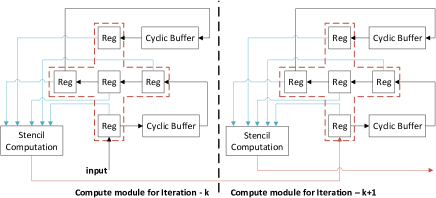
Another approach that can increase performance when mapping to FPGAs is to unroll the iterative loop, which encompasses one or more stencil loops over the rectangular mesh. This allows the results from a previous iteration to be fed to the next iteration without writing back to external (DDR4 or HBM) memory. This scheme, called the step-parallel technique in previous work [12] is illustrated in Fig. 2. The technique leads to increased throughput without the need for additional external memory bandwidth. However, the unrolling factor depends once more on available FPGA resources and internal memory capacity. Cutting down on external memory access in this manner also lead to more power-efficient designs. One disadvantage, however, is the increased length of the computational pipeline, which significantly affects performance for small mesh sizes.
III-A Model for the Baseline Design
The performance of a baseline design, as discuses above, therefore depends on (1) the capacity of the computational pipeline and (2) the external memory bandwidth. Computational capacity depends on the number of mesh point updates done in parallel (vectorization factor), latency of the pipeline and operating clock frequency of the FPGA. However, memory throughput depends on various factors such as the number of mesh elements transferred, and the stride between each transferred element. To simplify, we model reading/writing of contiguous data from/to memory with a maximum transfer size of 4K bytes, to reach a near optimal throughput of external/near-chip memory for the Xilinx U280 FPGA, our target hardware in this work.
Assuming that the memory throughput is sufficient to supply mesh points (i.e. a vectorization factor of ) continuously without interruption, then the total clock cycles taken to process a row from a 2D mesh with elements will be given by . Here, we have padded each row to be a multiple of if required. The compute pipeline will process rows as there are different rows between the current stencil update mesh point and farthest mesh point required for the stencil computation, where is the stencil order. If the outer iterative loop unroll factor is given by then the total number of clock cycles required to process the full mesh for iterations is given by:
| (2) |
The above extends naturally to 3D meshes as in (3), where the 3D mesh size is given by and is then equivalent to the number of plains to be buffered.
| (3) |
As noted before, the models above only hold for cases where the vectorization factor , which determines the number of parallel mesh points computed, does not demand more memory bandwidth than what can be supplied by the FPGA’s external DDR4 bandwidth. The FPGA’s HBM memory can be used to support a larger , which could then be limited by the resources available to implement the parallel compute pipelines. An estimate of maximum for an application can be computed by, using the FPGA operating frequency , and maximum supported bandwidth of a data channel (or port) on the FPGA, , and the size in bytes of a mesh element as follows:
| (4) |
For 2D meshes, if the width of the mesh is a multiple of vectorization factor V, then clock cycles for computing a single mesh point (or a cell) per iteration per compute module can be obtained from equation (2) as :
| (5) |
Setting to higher values gives a better clock cycles per mesh point ratio, the ideal being, . But higher order stencil applications on meshes with fewer rows will have a larger value, indicating idling in the processing pipeline. We explore techniques to reduce this idle time in Section IV-B.
A key parameter in (2) and (3) is the loop unroll factor, which directly determines performance, where a large reduces the total clock cycles required. However, is limited by the available resources on the FPGA as in Fig. 2, a larger requires more DSP blocks and LUTs. Furthermore, the internal memory required for a compute module, primarily due to memory capacity for the cyclic buffers also determines . The number of DSP blocks required for a single mesh-point update, depends on the stencil loop kernel’s arithmetic operations and number representation. Here we consider single precision floating point. With a vectorization factor, the total consumed is . If the total available DSP blocks on the FPGA is then the maximum unroll factor based on DSP resources, is given by:
| (6) |
The internal memory requirement for a single compute module which performs a order stencil operation on an mesh is . If the total available internal memory on the device is , then maximum possible iterative unroll factor based on internal memory requirements, is :
| (7) |
Here, is the size of a mesh element in bytes. The denominator of (7) becomes for 3D meshes. Thus we see that the internal memory of an FPGA, directly limits the solvable mesh size. Usually, the above ideal depth is not achievable, as the FPGA internal memory, BRAMs and URAMs, are quantized (for example BRAMs are 18Kb/36Kb and URAMs are 288Kb on the U280). Additionally, the limited width configurations of the URAMs, plus the need to allow for flexible routing further reduces the effective internal memory resources. Thus we usually target an 80%–90% internal memory utilization. Then the maximum iterative loop unroll factor is given by the minimum of and . It is also worth considering that a larger pipeline depth, and hence more resource consumption leads to the design spreading over multiple SLRs. Communication between SLRs increasing routing congestion between these regions, directly impacting the achievable operating frequency.
IV Optimizations
Further optimizations and extensions are required to obtain high throughput for more complex applications. These include (1) spatial and temporal blocking, specifically for solvers over larger meshes, and (2) batching for improving performance and throughput of stencil applications on smaller meshes. In this section, we build on the baseline design from Section III and extend the performance models to account for these optimizations.
IV-A Spatial and Temporal Blocking
The baseline design attempts to obtain perfect data reuse, requiring FPGA internal memory (consisting of BRAMs and URAMs) to be of size for 2D and for 3D meshes. Equation (7) illustrates this, where the requirement becomes highly limiting for applications with higher order () stencils and/or on larger meshes (increasing ). Even if the mesh fully fits in the FPGA’s DDR4 memory, a sufficiently large mesh could result in a less than one, meaning that even a single compute module cannot be synthesized. A solution is to implement a form of spatial blocking, similar to cache blocking tiling on CPUs, for the FPGA.
The idea is to use the baseline design to build an accelerator that operates on a smaller block of mesh elements and then transfer one such block at a time to the compute pipeline from FPGA DDR4 memory. The compute pipeline is designed with an appropriate vectorization factor () and an outer iterative loop unroll factor (). Larger results in better exploitation of temporal locality, where the execution uses the same data several times. One issue with such a blocked execution is when applying the computation over the boundary of a block where a stencil computation on the boundary will not have the contributions from all the neighboring elements in the mesh. The solution is to overlap blocks such that the correct computation is carried out on the boundary by a subsequent block. The amount of overlap depends on the order of the stencil. Overlapping leads to redundant computation. However this overhead can be acceptable, due to the savings from further exploiting local data in multiple iterations.
The main challenge of tiling then is to get close to maximum DDR4 memory bandwidth, due to the latency of smaller, non-contiguous data transfer sizes. Such data transfers results due to a strided access pattern in one dimension when accessing memory locations within a spatial block. For example on the Xilinx U280, it takes 16 clock cycles to transfer 1024 Bytes via the 512 bit wide AXI interface bus, but the latency of the transfer is about 14 clock cycles. As such, multiple read/write requests should be made to hide the latency of each individual memory transaction. The preference to maintain a 512 bit wide bus interface to obtain better memory bandwidth further increases the amount of redundant computation at block boundaries as we must maintain a 512 bit alignment in read/write transactions, regardless of the order of the stencil.
A final modification is the need to loop through the spatial blocks to solve over the full mesh. This control loop is best implemented on the FPGA to reduce latency due to the host calling multiple kernels on the FPGA. An important consideration is finding the optimal block size and its offset from the start of the mesh. The block size and offsets need only be computed once, which can be done on the host and copied to FPGA memory. Considering a 3D stencil application over a mesh of size solved by computing over with blocks (or tiles) of size , the valid number of mesh points computed per block is given by:
| (8) |
Since the number of clock cycles required to process iterations (or a temporal block) on the spatial block is similar to the baseline design, the average time taken to compute one block (assuming block dimensions are a multiple of ) would be:
| (9) |
Dividing (8) by (9) leads to the number of valid mesh points (or cells) computed per clock cycle (i.e. throughput, ) :
| (10) |
Now, substituting from (7), for a 3D application, assuming full utilization of the FPGA’s internal memory by a block, it can be shown that maximum throughput can be achieved for a given when :
| (11) |
The corresponding , can be shown to be also equal to , implying a square block to give the best throughput. However, the throughput also varies with and this can be analyzed by considering a square tile (i.e. ) applied to equation (10) and assuming to be very large such that is close to 1. With these assumptions, we can show that maximum throughput is achieved, for a given , when setting to a given by:
| (12) |
Obtaining a value for from (6), assuming we use all the computational capacity of the FPGA, we can rewrite (10) as:
| (13) |
The same for a 2D stencil application can also be derived as:
| (14) |
Here, we see that reducing pipeline depth and increasing will improve the performance of the spatial blocked design. The effect of is more significant for 3D applications.
IV-B Batching
A final optimization attempts to improve throughput for smaller mesh problems that usually perform poorly on accelerator platforms, including FPGAs. On traditional architectures such as GPUs the reason is the the under-utilization of the massive parallelism available. Essentially the time spent calling a kernel on the device and the overheads for data movement between host and device become dominate the actual processing time.
On an FPGA, in addition to the above, further overheads are caused due to the latency of the processing pipeline, as given in equation (5), compared to the time to process the mesh. The idle time is proportional to the width of the 2D mesh. Thus if a large number of smaller meshes are to be solved, as is the case in financial applications [26], then processing one mesh at a time incurs significant latencies. This motivates the idea of grouping together meshes with the same dimensions in batches, increasing the overall throughput of the solve. In practice, the mesh can be extended in the last dimension by stacking up the small meshes. Now, the inter-compute module latencies only occur once at the start of the batched solve. With , 2D meshes in a batch, the time to process a single mesh within a batched execution is given by:
| (15) |
Thus, increasing significantly reduces the idle time from (5). Similar reasoning can be applied for batched 3D meshes.
| FPGA | Xilinx Alveo U280 [27] |
|---|---|
| DSP blocks | 8490 |
| BRAM / URAM | 6.6MB (1487 blocks) / 34.5MB (960 blocks) |
| HBM | 8GB, 460GB/s, 32 channels |
| DDR4 | 32GB, 38.4GB/s, in 2 banks (1 channel/bank) |
| Host | Intel Xeon Silver 4116 @2.10GHz (48 cores) |
| 256GB RAM, Ubuntu 18.04.3 LTS | |
| Design SW | Vivado HLS, Vitis-2019.2 |
| GPU | Nvidia Tesla V100 PCIe [27] |
| Global Mem. | 16GB HBM2, 900GB/s |
| Host | Intel Xeon Gold 6252 @2.10GHz (48 cores) |
| 256GB RAM, Ubuntu 18.04.3 LTS | |
| Compilers, OS | nvcc CUDA 9.1.85, Debian 9.11 |
V Performance
In this section we apply the FPGA design strategy, optimizations, and extensions to illustrate their utility in accelerating stencil computations for explicit-iterative numerical solvers. We select three representative applications consisting of, both 2D and 3D, low and high order, and with single and multiple stencil loops to explore the versatility of our design flow. Model-predicted resource utilization estimates are used to determine initial design parameters, and runtime performance is compared to model predictions for each application. The implementations target the Xilinx Alveo U280 accelerator board and demonstrate concrete implementations for each application. We use Vivado C++ due to ease of use for configurations, arbitrary precision data types, and support of some C++ constructs compared to OpenCL, but note OpenCL can be equally used to implement the same design. Additionally, we compare equivalent implementations of each application’s performance on a modern GPU system for comparison111We have omitted CPU performance results here as our previous work [26] shows that GPUs provide significant speedups over CPUs for these applications. TABLE I briefly details the specifications of the FPGA and GPU systems (both hardware and software) used in our experiments.
V-A Poisson-5pt-2D
The first application is a 2D Poisson solver which uses a 2nd order stencil, with scalar elements:
| (16) |
A suitable initial vectorization factor can be identified by using (4) and assuming an operating frequency of 300MHz given this is the default set by the Vivado HLS tools. For a baseline implementation of Poisson a value of 8 for is calculated when using a single DDR4 channel or two HBM channels with a frequency of 300MHz. However, this frequency could only be supported when iterative loop unroll factor is in the order of 1– 20. Higher lead to routing congestion, which limited achievable frequency. As such the frequency was reduced to 250MHz to support a of 60, which we observed to give the best performance for this stencil. We find in some cases such a trial frequency adjustment is unavoidable, but our model significantly narrows the design space, enabling us to reason about and quickly obtain an optimal configuration. The number of DSP blocks required for a single mesh-point’s stencil computation for Poisson and the resulting from (6) for , assuming a 90% DSP utilization, is given in the first row of TABLE II.Column 4 gives the predicted from our performance model, while column 5 is the actual result after synthesis, indicating good agreement with the predicted design.
| Application | Freq. | |||
|---|---|---|---|---|
| (MHz) | (model) | (actual) | ||
| Poisson-5pt-2D | 250 | 14 | 68 | 60 |
| Jacobi-7pt-3D | 246 | 33 | 28 | 29 |
| Reverse Time Migration | 261 | 2444 | 3 | 3 |
| App. | Valid ratio | |||||
|---|---|---|---|---|---|---|
| Poisson-5pt-2D | 60 | 8 | 8192 | 472 | 98.5% | |
| Jacobi-7pt-3D | 3 | 64 | 768 | 768 | 189 | 98.4% |
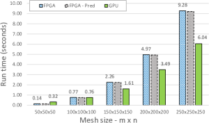
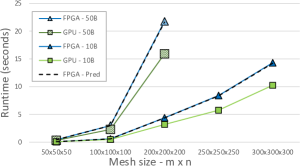
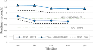
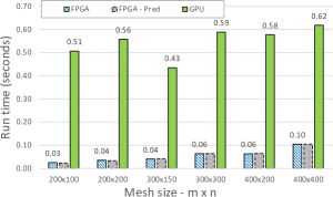
Figure 3 (a) and (b) present the runtime
performance of Poisson-5pt-2D, with the above design and compare the resultant
performance to an equivalent implementation on the
Nvidia V100 GPU. The achieved bandwidth and energy consumption from these
runs are summarized in TABLE IV. The bandwidth
is computed by counting the total number of bytes transferred during the
execution of the stencil loop (looking at the mesh data accessed) and dividing
it by the total time taken by the loop. Baseline FPGA performance is
significantly better than on the V100, since the GPU is not saturated by this
application. The batching of 2D meshes as in [26] improves
GPU performance significantly and offers a closer comparison. The FPGA achieves
a maximum speedup of about 30–34% for different mesh sizes and batching sizes
of 100 (100B) and 1000 (1000B). Memory bandwidth results indicate high
utilization of the communication channels in agreement with the observed
runtimes. The xbutil utility was used to measure power during FPGA
execution, while nvidi-smi was used for the same on the V100. The power
consumption of the FPGA during the 1000B runs is indicative of the significant
energy efficiency of the device compared to a GPU. The FPGA was operating at an
average 70W, while the GPU’s power consumption ranged from 40W (for single
batch) to 210W for 1000B runs on the larger meshes.
| Baseline and Batching (60000 iterations) | ||||||||
| Mesh | Baseline | 100B | 1000B | Energy-1000B | ||||
| FPGA | GPU | FPGA | GPU | FPGA | GPU | FPGA | GPU | |
| 384 | 18 | 857 | 404 | 867 | 530 | 0.77 | 3.48 | |
| 543 | 32 | 886 | 465 | 892 | 540 | 1.50 | 6.74 | |
| 535 | 38 | 901 | 483 | 907 | 560 | 1.66 | 7.60 | |
| 681 | 69 | 922 | 530 | |||||
| 612 | 62 | 889 | 536 | |||||
| 735 | 116 | 904 | 560 | |||||
| Spatial-blocking (60000 iterations) | |||||
| Mesh | Tile Size | BW | Energy | ||
| FPGA | GPU | FPGA | GPU | ||
| 1024 | 805 | 607 | 0.93 | 2.91 | |
| 4096 | 892 | 0.84 | |||
| 8000 | 905 | 0.83 | |||
| 1024 | 800 | 609 | 1.67 | 4.96 | |
| 4096 | 879 | 1.52 | |||
| 8000 | 907 | 1.48 | |||
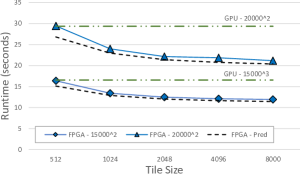
To implement Poisson-5pt-2D on larger meshes with spatial blocking, we assume a and equivalent to the baseline design and compute the valid mesh points updated per clock cycle using (13). Here we assume the dimensions of the mesh to be very large. TABLE III lists the model parameters for spatial blocking. For Poisson we see that the 2D spatially blocked designs theoretically perform similar to the baseline design and thus we need not change the compute pipeline. Runtime, bandwidth and energy consumption of this implementation is given in Figure 3 (c) and TABLE IV, respectively, including comparison to performance from the V100 GPU. Again we see good speedups and higher energy efficiency achieved with the FPGA, this time on large problem sizes with tiling.
V-B Jacobi-7pt-3D
The Jacobi iteration as a 3D, 7-point stencil, provides us with an initial, 3D, single stencil loop, for our evaluation:
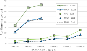
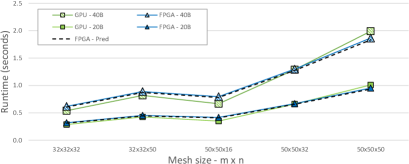
This application requires higher internal memory for the baseline design. For the spatially blocked design it involves transfers less than 4K from memory, which makes it difficult to approach raw external memory bandwidth. This is different to the baseline/batched and 2D spatially blocked design. We speculate that this could be the reason for the slightly less accurate model predictions in Figure 4(c). While the stencil is still fairly simple, now we see the GPU outperforming the FPGA conclusively, in both baseline, Figure 4(a) and batched Figure 4(b) tests. The V100 GPU gives nearly 40% faster runtimes on the 50B problem. However, the FPGA remains more energy efficient for the same problem. For the problem with 50B, it is nearly 2 more energy efficient than the faster GPU run (see TABLE V). The FPGA operated at an average 90W while the GPU power ranged from 77–240W. Spatial blocking was significantly more challenging and the resulting FPGA design, using a tile size was about 40% slower than the GPU runtime (see Figure 4(c)). However, the FPGA was again more energy efficient, operating at an average 70W consuming about 40–50% less energy than the GPU (operating at 180–216 W) as seen in TABLE V.
| Baseline (29k iters) and Batching (2.9k iters) | ||||||||
| Mesh | Baseline | 10B | 50B | Energy-50B | ||||
| FPGA | GPU | FPGA | GPU | FPGA | GPU | FPGA | GPU | |
| 202 | 83 | 307 | 284 | 323 | 404 | 0.04 | 0.07 | |
| 301 | 284 | 378 | 434 | 387 | 469 | 0.27 | 0.51 | |
| 374 | 496 | 421 | 548 | 426 | 543 | 1.96 | 3.77 | |
| 391 | 559 | 431 | 585 | |||||
| 403 | 553 | 438 | 569 | |||||
| Spatial-blocking (120 iterations) | |||||
| Mesh | Tile Size | BW | Energy | ||
| FPGA | GPU | FPGA | GPU | ||
| 256 | 233 | 392 | 0.062 | 0.106 | |
| 512 | 281 | 0.051 | |||
| 640 | 292 | 0.049 | |||
| 256 | 247 | 363 | 0.088 | 0.143 | |
| 512 | 270 | 0.080 | |||
| 640 | 273 | 0.079 | |||
V-C Reverse Time Migration (RTM) - Forward Pass
The final application we applied our development flow to is the forward pass from a Reverse Time Migration (RTM) solver [28]. The application represents algorithms of interest from industry [29], going beyond simple single stencil loops. It includes an iterative loop consisting of multiple stencil loops as summarized in Algorithm 1. and are 3D floating-point (SP) data arrays defined on the mesh consisting of vector elements of size 6. holds current values and holds intermediate values, both updated with the function which uses a 25-point, eighth order 3D stencil. is accessed/updated with a self-stencil (or zeroth-order, i.e. ). and are two 3D scalar coefficient meshes, which are also accessed using a self-stencil.
This application is significantly more complex than the previous applications and pushes the resource usage on the FPGA to its limits. Nevertheless our design strategy is able to provide a good implementation, albeit limited to a batched design. The number of stencil loops was reduced by fusing the and with the corresponding loop. The and final update were merged into one further loop, resulting in a total of 4 loops. For an FPGA implementation, all the four fused loops needed to be brought into a single pipeline. Intermediate data and were replaced with a FIFO stream connected through window buffers. Similarly and were internally buffered and fed to subsequent compute units. These optimizations reduce the number of memory accesses to a single read and write of and a single read each for and . These are significant savings compared to the original loop chain.
A limitation of the FPGA implementation is that the mesh plane size (in this 3D application), is limited to as it uses 3D stencils on a 6 dimensional element (i.e. a vector of 6 floats). Furthermore, partitioning four compute-intensive kernels on the U280’s three SLR regions was a significant challenge. Our implementation avoids spanning of a compute unit on multiple SLRs to avoid inter SLR routing congestion, by setting to 1, allowing us to fit the four fused loops in one SLR. This, then allows for an iterative loop unroll factor of 3 () given the three SLRs on the U280. We do note that using more HBM channels could provide more bandwidth to obtain a larger , but we have not explored this in current work. A solution for the limited mesh size is of course spatial blocking, but it requires . This leads to a tile size dimension from (12) given is 8, which requires a large amount of FPGA internal memory, making an implementation on the U280 challenging as the four fused loops will span across SRLs. We leave this to future work.
| Baseline (1800 iters) and Batching (180 iters) | ||||||||
| Mesh | Baseline | 20B | 40B | Energy-40B | ||||
| FPGA | GPU | FPGA | GPU | FPGA | GPU | FPGA | GPU | |
| 108 | 130 | 225 | 251 | 232 | 266 | 0.043 | 0.086 | |
| 141 | 163 | 247 | 263 | 253 | 274 | 0.062 | 0.133 | |
| 77 | 124 | 210 | 251 | 220 | 263 | 0.055 | 0.111 | |
| 127 | 155 | 262 | 266 | 270 | 272 | 0.091 | 0.218 | |
| 165 | 179 | 287 | 271 | 293 | 275 | 0.130 | 0.338 | |
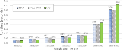
From the runtime results in Figure 5 and bandwidth results in TABLE VI we see that the FPGA implementation is either matching or marginally better performing than the GPU. Note that, given there are four stencil loops fused on the FPGA the bandwidth reported is for the fused loop. The GPU bandwidth therefore is the average for the full loop chain. The most time consuming kernel, on the GPU achieved around 180 GB/s, while the highest bandwidth achieved by a single kernel is over 340GB/s. Again we see that the FPGA operates at a lower average power (70W) than the GPU (51–170W) consuming 2 less energy.
VI Conclusions
In this paper we developed a unified workflow and a supporting predictive analytic model for FPGA synthesis of structured-mesh stencil applications that combines standard state-of-the-art techniques with a number of high-gain optimizations targeting features of real-world work loads. The model allows estimation of design parameters, resource usage, and performance for performant FPGA implementation. The workflow was applied to three representative applications, implemented on a Xilinx Alveo U280 FPGA. Performance was compared to highly-optimized HPC-grade Nvidia V100 GPU code. In most cases, the FPGA is able to match or improve on GPU performance. However, even when runtime is inferior to the GPU, significant energy savings, over 2 for the largest application, are observed. Estimations produced by the model were shown to be accurate and a good guide in the design process. Future work will investigate how a similar workflow can be applied to implicit solvers and further automating the development of this class of application on FPGAs, including alternative numerical representations. The FPGA and GPU source code developed in this paper are available at [30].
Acknowledgment
Gihan Mudalige was supported by the Royal Society Industry Fellowship Scheme(INF/R1/1800 12). István Reguly was supported by National Research, Development and Innovation Fund of Hungary, project PD 124905, financed under the PD_17 funding scheme. The authors would like to thank Jacques Du Toit and Tim Schmielau at NAG UK Ltd., for the RTM application and for their valuable advice.
References
- [1] D. B. Cousins, K. Rohloff, and D. Sumorok, “Designing an FPGA-accelerated homomorphic encryption co-processor,” IEEE Transactions on Emerging Topics in Computing, vol. 5, no. 2, pp. 193–206, 2016.
- [2] M. Owaida, D. Sidler, K. Kara, and G. Alonso, “Centaur: A framework for hybrid CPU-FPGA databases,” in Proceedings of the IEEE International Symposium on Field-Programmable Custom Computing Machines (FCCM), 2017, pp. 211–218.
- [3] C. Wang, L. Gong, Q. Yu, X. Li, Y. Xie, and X. Zhou, “DLAU: A scalable deep learning accelerator unit on FPGA,” IEEE Transactions on Computer-Aided Design of Integrated Circuits and Systems, vol. 36, no. 3, pp. 513–517, 2016.
- [4] T. Becker, O. Mencer, S. Weston, and G. Gaydadjiev, “Maxeler data-flow in computational finance,” in FPGA Based Accelerators for Financial Applications, 2015, pp. 243–266.
- [5] S. A. Fahmy, K. Vipin, and S. Shreejith, “Virtualized FPGA accelerators for efficient cloud computing,” in Proceedings of the IEEE International Conference on Cloud Computing Technology and Science (CloudCom), 2015, pp. 430–435.
- [6] I. Z. Reguly, G. R. Mudalige, and M. B. Giles, “Loop tiling in large-scale stencil codes at run-time with OPS,” IEEE Transactions on Parallel and Distributed Systems, vol. 29, no. 4, pp. 873–886, April 2018.
- [7] G. R. Mudalige, M. B. Giles, I. Z. Reguly, C. Bertolli, and P. H. J. Kelly, “OP2: An active library framework for solving unstructured mesh-based applications on multi-core and many-core architectures,” 2012 Innovative Parallel Computing, InPar 2012, 2012. [Online]. Available: http://dx.doi.org/10.1109/InPar.2012.6339594
- [8] P. Vincent, F. Witherden, B. Vermeire, J. S. Park, and A. Iyer, “Towards green aviation with python at petascale,” in SC16: International Conference for High Performance Computing, Networking, Storage and Analysis, Nov 2016, pp. 1–11.
- [9] F. Luporini, M. Lange, M. Louboutin, N. Kukreja, J. Hückelheim, C. Yount, P. Witte, P. H. J. Kelly, F. J. Herrmann, and G. J. Gorman, “Architecture and performance of Devito, a system for automated stencil computation,” CoRR, vol. abs/1807.03032, Jul 2018. [Online]. Available: http://arxiv.org/abs/1807.03032
- [10] H. Fu and R. G. Clapp, “Eliminating the memory bottleneck: An FPGA-based solution for 3D reverse time migration,” in Proceedings of the 19th ACM/SIGDA International Symposium on Field Programmable Gate Arrays, ser. FPGA ’11. New York, NY, USA: Association for Computing Machinery, 2011, p. 65–74. [Online]. Available: https://doi.org/10.1145/1950413.1950429
- [11] P. Rawat, M. Kong, T. Henretty, J. Holewinski, K. Stock, L.-N. Pouchet, J. Ramanujam, A. Rountev, and P. Sadayappan, “SDSLc: A multi-target domain-specific compiler for stencil computations,” in Proceedings of the 5th International Workshop on Domain-Specific Languages and High-Level Frameworks for High Performance Computing, ser. WOLFHPC ’15. New York, NY, USA: Association for Computing Machinery, 2015. [Online]. Available: https://doi.org/10.1145/2830018.2830025
- [12] H. M. Waidyasooriya, Y. Takei, S. Tatsumi, and M. Hariyama, “OpenCL-based FPGA-platform for stencil computation and its optimization methodology,” IEEE Transactions on Parallel and Distributed Systems, vol. 28, no. 5, pp. 1390–1402, 2017.
- [13] Y. Chi, J. Cong, P. Wei, and P. Zhou, “SODA: Stencil with pptimized dataflow architecture,” in 2018 IEEE/ACM International Conference on Computer-Aided Design (ICCAD), 2018, pp. 1–8.
- [14] H. R. Zohouri, A. Podobas, and S. Matsuoka, “Combined spatial and temporal blocking for high-performance stencil computation on FPGAs using OpenCL,” in Proceedings of the 2018 ACM/SIGDA International Symposium on Field-Programmable Gate Arrays, ser. FPGA ’18. New York, NY, USA: Association for Computing Machinery, 2018, p. 153–162. [Online]. Available: https://doi.org/10.1145/3174243.3174248
- [15] H. R. Zohouri, A. Podobas, and S. Matsuoka, “High-performance high-order stencil computation on FPGAs using OpenCL,” in 2018 IEEE International Parallel and Distributed Processing Symposium Workshops (IPDPSW), 2018, pp. 123–130.
- [16] H. M. Waidyasooriya and M. Hariyama, “Multi-FPGA accelerator architecture for stencil computation exploiting spacial and temporal scalability,” IEEE Access, vol. 7, pp. 53 188–53 201, 2019.
- [17] Y.-H. Lai, Y. Chi, Y. Hu, J. Wang, C. H. Yu, Y. Zhou, J. Cong, and Z. Zhang, “HeteroCL: A multi-paradigm programming infrastructure for software-defined reconfigurable computing,” in Proceedings of the 2019 ACM/SIGDA International Symposium on Field-Programmable Gate Arrays, ser. FPGA ’19. New York, NY, USA: Association for Computing Machinery, 2019, p. 242–251. [Online]. Available: https://doi.org/10.1145/3289602.3293910
- [18] K. Dohi, K. Fukumoto, Y. Shibata, and K. Oguri, “Performance modeling and optimization of 3D stencil computation on a stream-based FPGA accelerator, year=2013, pages=1-6,” in 2013 International Conference on Reconfigurable Computing and FPGAs (ReConFig).
- [19] G. Natale, G. Stramondo, P. Bressana, R. Cattaneo, D. Sciuto, and M. D. Santambrogio, “A polyhedral model-based framework for dataflow implementation on FPGA devices of iterative stencil loops,” in 2016 IEEE/ACM International Conference on Computer-Aided Design (ICCAD), 2016, pp. 1–8.
- [20] K. Sano, Y. Hatsuda, and S. Yamamoto, “Multi-FPGA accelerator for scalable stencil computation with constant memory bandwidth,” IEEE Transactions on Parallel and Distributed Systems, vol. 25, no. 3, pp. 695–705, 2014.
- [21] M. Shafiq, M. Pericàs, R. de la Cruz, M. Araya-Polo, N. Navarro, and E. Ayguadé, “Exploiting memory customization in FPGA for 3D stencil computations,” in 2009 International Conference on Field-Programmable Technology, 2009, pp. 38–45.
- [22] M. Schmidt, M. Reichenbach, and D. Fey, “A generic VHDL template for 2D stencil code applications on FPGAs,” in 2012 IEEE 15th International Symposium on Object/Component/Service-Oriented Real-Time Distributed Computing Workshops, 2012, pp. 180–187.
- [23] K. Sano, Y. Hatsuda, and S. Yamamoto, “Scalable streaming-array of simple soft-processors for stencil computations with constant memory-bandwidth,” in 2011 IEEE 19th Annual International Symposium on Field-Programmable Custom Computing Machines, 2011, pp. 234–241.
- [24] J. de Fine Licht, A. Kuster, T. D. Matteis, T. Ben-Nun, D. Hofer, and T. Hoefler, “StencilFlow: mapping large stencil programs to distributed spatial computing systems,” 2020. [Online]. Available: https://arxiv.org/abs/2010.15218
- [25] “Xilinx - large fpga methodology guide,” 2012, https://www.xilinx.com/support/documentation/sw_manuals/xilinx14_7/ug872_largefpga.pdf.
- [26] I. Z. Reguly, B. Moore, T. Schmielau, J. du Toit, and G. R. Mudalige, “Batch solution of small PDEs with the OPS DSL,” in High Performance Computing, M. Weiland, G. Juckeland, S. Alam, and H. Jagode, Eds. Cham: Springer International Publishing, 2019, pp. 124–141.
- [27] Alveo U280 data center accelerator card data sheet, Xilinx Inc., May 2020, v1.3.
- [28] R. Clayton and B. Engquist, “Absorbing boundary conditions for acoustic and elastic wave equations,” Bulletin of the Seismological Society of America, vol. 67, no. 6, pp. 1529–1540, 12 1977.
- [29] “Discussions with the Numerical Algorithms Group, UK.” 2019-2020.
- [30] “High-Level FPGA accelerator design for structured-mesh-based explicit numerical solvers - GitHub Code Repository,” 2020, https://github.com/Kamalavasan/StencilsOnFPGA.