Understanding Power Consumption and Reliability of High-Bandwidth Memory with Voltage Underscaling
Seyed Saber Nabavi Larimi1,2 Behzad Salami1,5 Osman S. Unsal1
Adrián Cristal Kestelman1,2,3 Hamid Sarbazi-Azad4 Onur Mutlu5
1BSC 2UPC 3CSIC-IIIA 4SUT and IPM 5ETH Zürich
Abstract
Modern computing devices employ High-Bandwidth Memory (HBM) to meet their memory bandwidth requirements. An HBM-enabled device consists of multiple DRAM layers stacked on top of one another next to a compute chip (e.g. CPU, GPU, and FPGA) in the same package. Although such HBM structures provide high bandwidth at a small form factor, the stacked memory layers consume a substantial portion of the package’s power budget. Therefore, power-saving techniques that preserve the performance of HBM are desirable. Undervolting is one such technique: it reduces the supply voltage to decrease power consumption without reducing the device’s operating frequency to avoid performance loss. Undervolting takes advantage of voltage guardbands put in place by manufacturers to ensure correct operation under all environmental conditions. However, reducing voltage without changing frequency can lead to reliability issues manifested as unwanted bit flips.
In this paper, we provide the first experimental study of real HBM chips under reduced-voltage conditions. We show that the guardband regions for our HBM chips constitute 19% of the nominal voltage. Pushing the supply voltage down within the guardband region reduces power consumption by a factor of 1.5X for all bandwidth utilization rates. Pushing the voltage down further by 11% leads to a total of 2.3X power savings at the cost of unwanted bit flips. We explore and characterize the rate and types of these reduced-voltage-induced bit flips and present a fault map that enables the possibility of a three-factor trade-off among power, memory capacity, and fault rate.
Index Terms:
High-Bandwidth Memory, Power Consumption, Voltage Scaling, Fault Characterization, Reliability.I Introduction
Dynamic Random Access Memory (DRAM) is the predominant main memory technology used in traditional computing systems. With the significant growth in the computational capacity of modern systems, DRAM has become a power/performance/energy bottleneck, especially for data-intensive applications [12, 38, 39, 37, 15]. There are two approaches to alleviate this issue: (i) replacing DRAM with emerging technologies (e.g., Magnetic Memory (MRAM) [40, 24] and Phase-Change Memory (PCM) [46, 25, 47]) and (ii) improving DRAM design (e.g., Reduced Latency DRAM (RLDRAM) [52], Graphics DDR (GDDR) [18], and Low-Power DDR (LPDDR) [33]). To the latter end, High-Bandwidth Memory (HBM) [27, 26] has been developed to bridge the bandwidth gap of computing devices and DRAM-based main memory.
An HBM-enabled device consists of multiple DRAM layers stacked and placed next to computing elements, all integrated in the same package. Higher bandwidth, lower power consumption, and smaller form factor are the advantages of such integration. Therefore, despite being a relatively new technology, HBM has found its way into high-end devices such as NVIDIA A100 [41], Xilinx Virtex Ultrascale+ HBM family [66], and AMD Radeon Pro family [48], and into some of the world’s fastest computing systems such as the Summit supercomputer [21]. However, being placed inside the same package with computing devices means that HBM consumes a portion of the package’s overall power budget, limiting the power available for computing devices. Since HBM targets high-performance applications, any power saving technique with bandwidth overhead is undesirable. Therefore, there is a need for methods that save power without reducing the bandwidth.
Undervolting, also called voltage underscaling, lowers supply voltage without decreasing operating frequency, thereby saving power without affecting performance. In real devices, undervolting is effective because manufacturers conservatively specify a higher supply voltage for the operation of a device than the minimum necessary supply voltage for correct operation. The difference between the default supply voltage and this minimum supply voltage is called “guardband”. Guardbands are put in place to ensure correct and consistent operation under all possible (including worst-case) operating conditions. Pushing the supply voltage down in the guardband region reduces power consumption.
We obtain 1.5X power savings in real HBM chips under all bandwidth utilization rates by reducing the supply voltage from the nominal 1.2V down to 0.98V, safely without any faults under common operating conditions. Pushing the supply voltage further down to 0.85V, results in an overall 2.3X power savings. However, at voltages below the guardband region, device components start experiencing timing violations, causing unwanted bit flips. In our experiments, first bit flips occur at 0.97V. From 0.97V to 0.84V, the number of faults increases exponentially until almost all bits are faulty. Between 0.84V and 0.81V, all bits become faulty, while using voltages lower than 0.81V result in the failure of entire HBM chips. To save power with undervolting, we need to understand the occurrence rate of faults at each voltage level, if and how faults are clustered and how far we can lower the supply voltage below the guardband region.
Undervolting has been experimentally studied on CPUs [43, 71, 51, 2], GPUs [30, 29, 28, 70] and FPGAs [56, 60, 54], as well as DRAMs [12, 13, 19, 14], SRAMs [68, 67], and NAND flash memories [4, 9, 5, 6, 7, 10, 36, 8]. Our work is the first experimental study of undervolting HBM chips. Our main contributions are as follows:
-
•
We empirically measure a 19% voltage guardband in HBM chips. We show that undervolting within the guardband region reduces HBM power consumption by a factor of 1.5X.
-
•
We empirically examine undervolting below the guardband region in HBM chips and demonstrate a total of 2.3X power savings at the cost of some unwanted bit flips.
-
•
We provide the first experimental fault characterization study of HBM undervolting below the guardband region. We find that (i) HBM channels behave differently from each other with voltage underscaling due to process variation, and (ii) most faults are clustered together in small regions of HBM layers.
-
•
We provide a fault map that enables the user to perform a three-factor trade-off among power, fault-rate, and usable memory space. For instance, 2.3X power savings is possible by sacrificing some memory space while the remaining memory space can work with 0% to 50% fault rate.
II Experimental Methodology
II-A Background on HBM
Fig. 1(a) shows the general organization of an HBM-enabled device where several DRAM chips (and an optional IO/controller chip) are piled and interconnected by Through Silicon Vias (TSVs) [27]. An efficient way to utilize an HBM stack is to place it on a silicon interposer next to computing chips (e.g., FPGA, GPU, or CPU) inside the same package [20]. Signals between HBM stack and computing chips go through the underlying silicon interposer. As a result, there can be far more data lanes in an HBM channel (1024 per HBM stack) than a regular 64-bit DRAM channel, while each HBM channel is more efficient. Therefore, HBM provides at least an order of magnitude higher bandwidth than DDRx DRAM [15] at a lower power consumption (nearly 7pJ/bit as opposed to 25pJ/bit for a DDRx DRAM) with a smaller form factor [65].
II-B Testing Platform
The hardware platform we use in our experiments consists of a Xilinx VCU128 board [62] mounted with an XCVU37P FPGA. This FPGA includes two HBM stacks of 4GB each (HBM0 and HBM1). Each stack has four DRAM chips of 1GB capacity each. Fig. 1(b) shows a general overview of the underlying HBM memory. The FPGA fabric is divided into three Super Logic Regions (SLRs). Each SLR is a separately fabricated chip with configurable circuitry. SLRs are interconnected by the same interposer technology connecting them to the HBM stacks. Both HBM stacks of our setup are connected to SLR0, as shown in Fig.1(b).
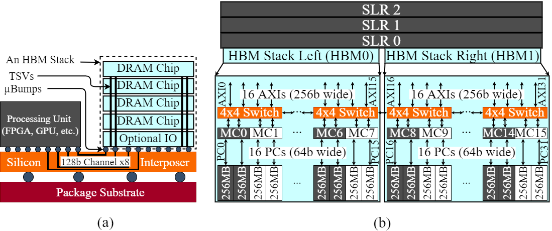
Address space of each HBM stack is divided among 8 independent Memory Channels (MC). Each MC is 128b wide and works independently on a 512MB memory assigned to it. Address space of each channel is divided between two 64b Pseudo-Channels (PCs). These two PCs share clock and command signals but have separate data buses. Each PC independently interprets commands and works with its own non-overlapping 256MB memory array portion. Therefore, at memory side, there are a total of 32 PCs, 64b wide each. At user side, Xilinx’s HBM IP core provides 32 AXI ports (16 per HBM stack). Each AXI port corresponds to one PC. However, if the switching network is enabled, any packet from an AXI port can be routed to any PC at the cost of extra delay and lower bandwidth. An AXI port is 256b wide, which provides a 4:1 data width ratio over a PC (with 64b width). As a result, an AXI port can operate at a clock frequency that is a quarter of the memory data transfer rate (1:4 ratio) and yet take advantage of the maximum HBM bandwidth provided by PCs [65]. The maximum clock frequency allowed for memory arrays in our device is 900MHz, and being a double data rate memory, it translates to a maximum data transfer rate of 1800 Mega-Transfers per second (MT/s).
In this work, we tune the supply voltage of our HBM stacks by accessing voltage regulators on the VCU128 board. One of these regulators, ISL68301, is a Power Management Bus (PMBus) [45] compliant driver from Intersil Corporation in charge of supplying power to our HBM stacks. We implemented a customized interface on the host to control this regulator and measure power, voltage and current during our experiments. We also implement controllers for the two HBM stacks. Each controller includes 16 AXI Traffic Generators (TG), one for each AXI port in that stack. The controller is in charge of configuring each TG, sending macro commands, receiving responses, checking status, and reporting statistics back to the host. Each TG is capable of running customized macro commands that we later use to implement our test routines. We collect power measurements from a Texas Instruments INA226 chip placed on VCU128 board.
II-C Experiments
We conduct experiments to measure (i) the power we can save with undervolting and (ii) the fault rate of our HBM devices when we reduce the voltage below the nominal value. The methodology we used for our experiments, considers the following points:
-
•
Since we focus on HBM stacks and not FPGA fabric, we disable the switching network. This removes any impact the switching network might have on the results.
-
•
We follow a statistical method to determine the number of runs based on error and confidence margin [31]. We run each test 130 times, which gives us a 7% error margin with 90% confidence interval.
-
•
HBM bandwidth is much larger than the communication speed between the FPGA and host CPU. As a result, we focus on measuring simple statistics on the FPGA itself and then report those raw numbers back to the host for further analysis.
-
•
The operating temperature of HBM stacks was 35 ±1°C during our experiments.
We conduct the following power and reliability experiments:
II-C1 Power Measurement Tests
We measure the power consumption of HBM stacks at different bandwidth utilization rates while underscaling their supply voltage. We reach nearly 310GB/sec when accessing the memory by enabling all 32 AXI ports at the same time and running them at maximum frequency.111The combined peak theoretical bandwidth of HBM stacks in VCU128 is 429GB/sec [62]. For the experiments discussed in this paper, we reach the throughput of 310GB/sec. However, we believe that with more engineering effort, the peak performance is also achievable. The power savings obtained via undervolting is achievable for any bandwidth utilization rate, as discussed in Section III. We then progressively disable AXI ports to reduce bandwidth. We do this since some AXI ports (and their corresponding PCs) that map to the more vulnerable HBM memory blocks are more sensitive to faults induced by undervolting than others. Therefore, disabling those ports is an effective technique to decrease the impact of undervolting faults and further reduce the supply voltage. Section III-B discusses variability across different ports in more details.
II-C2 Reliability Assessment
The fault characterization test we conduct writes data into the undervolted HBM sequentially and then reads it back to check for any faults. Algorithm 1 shows the pseudo-code of the reliability tester to extract . We change the HBM’s supply voltage (i.e., VCC_HBM) from 1.2V (the nominal voltage level, i.e., ) to 0.81V (minimum voltage possible for memory operation, i.e., ), with 10mV step size. We experimentally set the batchSize, the number of times we repeat each test to ensure consistent results, to 130. memSize is the size of the memory divided by 256b (i.e., width of an AXI port). By setting dataPattern to all 1’s or all 0’s, we can check for 1-to-0 or 0-to-1 bit flips, respectively. dataWidth is 256b since each AXI port is 256b wide. Depending on the type of the test, memSize takes different values, i.e., 256M or 8M for testing the entire HBM or a single Pseudo Channel (PC), respectively.
III Results
III-A Power Analysis
We divide the total power consumption of an HBM chip into active and idle portions.
III-A1 Active Power
Active power consumption of a DRAM chip is proportional to the square of supply voltage (), as shown in Equation (1) [11]. In this equation, is the active load capacitance, is operating frequency, and is the activity factor which determines the average charge/discharge rate of the capacitor. Thus, with undervolting, we expect a quadratic reduction in active power consumption.
| (1) |
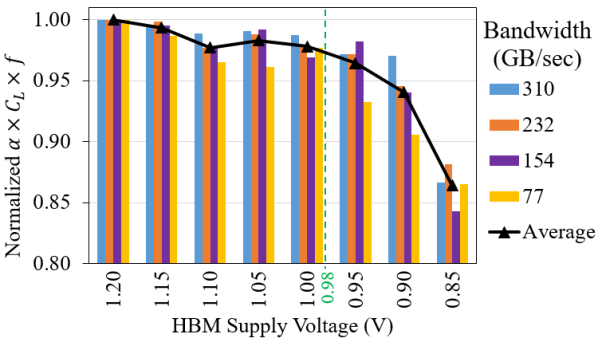
Our empirical results shown in Fig. 2 comply with expectations. Fig. 2 shows the power consumption of HBM chips at representative bandwidth utilization rates (in 25% increments).
Working within the guardband region (1.20V-0.98V), provides 1.5X power savings while pushing the supply voltage further down to 0.85V results in a total of 2.3X savings compared to default voltage 1.2V. In both cases (within or below the guardband region), the amount of power savings is independent of the bandwidth utilization because undervolting does not affect the memory bandwidth. Therefore, we can save the memory power by undervolting no matter what the memory bandwidth demand is.

On the other hand, looking at Equation (1), if we divide our power measurement results by , we are left with raw values for . The unit for these values is farads per second, which indicates how much capacitance is being actively charged/discharged every second. is constant since the clock frequency of HBM memory, and the sequence that we run these tests are always fixed. , on the other hand, depends on the memory bandwidth utilization rate, which we expect to remain fixed when working at a fixed bandwidth (i.e., same number of PCs). As a result, we expect values for to remain the same throughout our experiments. However, through undervolting, we observe that HBM chips’ fidelity starts to degrade. This is because at voltages lower than 0.98V (i.e., below the guardband region), some bits remain always stuck at 0 or 1. Since memory operations cannot charge or discharge these faulty bits anymore, such bits do not contribute to the overall active capacitance, resulting in a drop in . We show this behavior in Fig. 3: for supply voltages above 0.98V, remains within 3% of what we expect. However, below 0.98V, it starts dropping and at 0.85V it reaches 14% lower than the maximum active capacitance (at nominal voltage). In other words, undervolting below the guardband region leads to a lower active capacitance, as shown in Fig. 3. This is due to the exponential increase of fault rate in HBM memory, as discussed in Section III-B.
III-A2 Idle Power
To evaluate idle power savings, we measure the power consumption of HBM when bandwidth utilization is zero. We find that even when HBM is idle, it consumes nearly one-third of the power it consumes at full load with 100% bandwidth utilization, limiting the maximum amount of power we can save. As seen in Fig. 2, idle power gradually reduces with undervolting.

III-B Reliability Analysis
III-B1 Overall Analysis
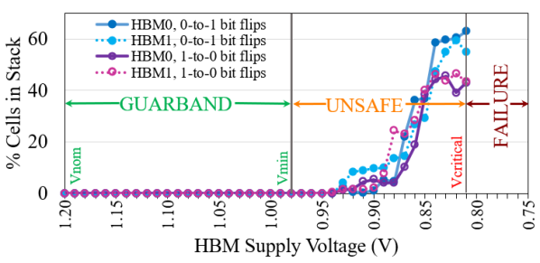
Fig. 4 shows the behavior of each HBM stack with undervolting. We observe the followings:
-
•
Guardband Region: Starting from the nominal voltage (=1.2V) down to the minimum safe voltage (=0.98V), we observe no memory faults. This guardband region is safe for all operations and workloads. An application that cannot tolerate any fault in memory has to work in this region.
-
•
Unsafe Region: Faults occur in voltages below . Any application that uses HBM with supply voltages in the unsafe region needs to take the impact of such faults into account to ensure correct operation. Reducing the voltage introduces new faults with an exponentially growing trend until about 0.84V, where all memory bits experience 0-to-1 or 1-to-0 bit flips. Other works have reported similar exponential growth of faults with undervolting on regular DDRx DRAM chips [12]. Below 0.84V down to the minimum working voltage (=0.81V), the entire HBM parts become faulty.
-
•
In our tests, HBM crashes (i.e., stops responding) at voltages below . Even restoring the supply voltage does not re-enable operation, and a power-down and restart is required.
III-B2 Detailed Analysis of Fault Rate Variation
Fig. 5 shows the fault rate for each HBM chip, each AXI port (and its corresponding PC), and each data pattern at supply voltage levels below . Due to process variation and noise in memory, we observe three categories of fault rate/type variation:
-
•
Variation Across HBM Chips: In the unsafe voltage range (i.e., between and ), HBM0 has lower fault rate than HBM1 (13% on average). However, both stacks have the same and .
-
•
Variation Across PCs: Some PCs are more sensitive to undervolting than others (e.g., PC4 and PC5 of HBM0 and PC18, PC19, and PC20 of HBM1). These PCs experience a higher rate of bit flips when we reduce the voltage below .
-
•
Data Pattern Variation: The first 1-to-0 and 0-to-1 bit flips start at 0.97V and 0.96V, respectively. The average rate of 0-to-1 bit flips is 21% higher than that of 1-to-0 bit flips.
III-C User- and Application-Level Implications
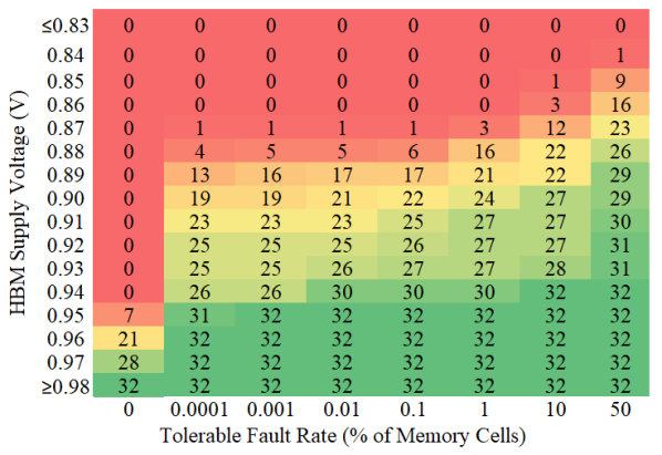
Applications that are intrinsically resilient to faults can save more power than others by taking advantage of aggressive undervolting even below the guardband region. To effectively achieve this benefit, application developers need practical information about the effects of undervolting. To this end, we present a three-factor trade-off among power, fault rate, and available memory capacity that helps application developers determine how much power can be saved and what the associated costs are.
An HBM chip has multiple independently-controllable PCs (32 in our case). We utilize this inherent independence to provide practical information about how many PCs an application can use based on its tolerable fault rate, as shown in Fig. 6. For example:
- •
-
•
Below , a triple-factor trade-off is at the user’s disposal. For example, up to 1.6X power savings is achievable for an application that cannot tolerate any faults but can work with smaller memory capacity, by using only 7 fault-free PCs operating at 0.95V.
-
•
Applications that can tolerate a non-zero fault rate (e.g., [23, 54, 22, 34]) allow more room for trade-offs. For example, an application that can tolerate a 0.0001% fault rate and requires only half of the total memory capacity can push the voltage down to 0.90V and save power by a factor of about 1.8X.
IV Related Work
To our best knowledge, this paper presents the first experimental study of undervolting in real High-Bandwidth Memory (HBM) chips. Below, we briefly cover closely-related work on reduced-voltage operation in other computing and memory devices.
- •
-
•
Hardware Accelerators: Undervolting in FPGAs has recently been studied [17, 53, 56, 57, 54, 60, 58]. These studies focus on undervolting multiple components of FPGAs (e.g., Block RAMs (BRAMs) and internal components). Undervolting in GPUs is also studied with detailed analysis of power saving, voltage guardbands, and reliability costs [70, 28, 30, 29].
-
•
Memory Chips: Koppula et al. [23] propose a DRAM undervolting and latency reduction framework for neural networks that improves energy efficiency and performance of such networks by 37% and 8%, respectively. Chang et al. [12] study the impact of undervolting on the reliability and energy consumption of DRAM by characterizing faults in real DRAM chips and provide techniques to mitigate undervolting-induced faults. Earlier works study undervolting in main memory systems [13, 14], but do not analyze faults due to undervolting. Ghose et al. [16] study power consumption in modern DRAM chips. Luo et al. [34] show that unreliable DRAM chips can be used in real applications to enhance the cost of scaling the main memory system. Undervolting is also studied for other memory types like SRAM [68, 67] and flash [4, 9, 5, 6, 7, 10, 36, 8].
V Conclusion
We reported the first undervolting study of real High-Bandwidth Memory (HBM) chips. We demonstrated 1.5X to 2.3X power savings for such chips via voltage underscaling below the nominal level. We measured a voltage guardband of 19% of the nominal voltage, and showed that eliminating it results in 1.5X power savings. We discussed that further undervolting below the guardband region provides more power savings, at the cost of unwanted bit flips in HBM cells. We explored and characterized the behavior of these bit flips (e.g., rate, type, and variation across memory channels) and presented a fault map that enables the possibility of a three-factor trade-off between power, memory capacity, and fault rate. We conclude that undervolting for High-Bandwidth Memory chips is very promising for future systems.
Acknowledgments
The research leading to these results has received funding from the European Union’s Horizon 2020 Programme under the LEGaTO Project (www.legato-project.eu), grant agreement No. 780681. This work has received financial support, in part, from Tetramax for the LV-EmbeDL project. This work is supported in part by funding from SRC and gifts from Intel, Microsoft and VMware to Onur Mutlu.
References
- [1] A. Alameldeen “Energy-Efficient Cache Design Using Variable-Strength Error-Correcting Codes” In ISCA, 2011
- [2] A. Bacha “Dynamic Reduction of Voltage Margins by Leveraging On-Chip ECC in Itanium II Processors” In ISCA, 2013
- [3] R. Bertran “Voltage Noise in Multi-Core Processors: Empirical Characterization and Optimization Opportunities” In MICRO, 2014
- [4] Y. Cai “Error Analysis and Retention-Aware Error Management for NAND Flash Memory” In Intel Technology Journal (ITJ), 2013
- [5] Y. Cai “Error Characterization, Mitigation, and Recovery in Flash-Memory-based Solid-State Drives” In Proc. IEEE, 2017
- [6] Y. Cai “Error Patterns in MLC NAND Flash Memory: Measurement, Characterization, and Analysis” In DATE, 2012
- [7] Y. Cai “Read Disturb Errors in MLC NAND Flash Memory: Characterization, Mitigation, and Recovery” In DSN, 2015
- [8] Y. Cai “Reliability Issues in Flash-Memory-Based Solid-State Drives: Experimental Analysis, Mitigation, Recovery” In Proc. Springer, Inside Solid State Drives (SSDs), 2018
- [9] Y. Cai “Threshold Voltage Distribution in MLC NAND Flash Memory: Characterization, Analysis, and Modeling” In DATE, 2013
- [10] Y. Cai “Vulnerabilities in MLC NAND Flash Memory Programming: Experimental Analysis, Exploits, and Mitigation Techniques” In HPCA, 2017
- [11] “Calculating Memory Power for DDR4 SDRAM” In Technical Report, Micron Technology, Inc., 2017
- [12] K. Chang “Understanding Reduced-voltage Operation in Modern DRAM Devices: Experimental Characterization, Analysis, and Mechanisms” In POMACS, 2017
- [13] H. David “Memory Power Management via Dynamic Voltage/Frequency Scaling” In ICAC, 2011
- [14] Q. Deng “MemScale: Active Low-power Modes for Main Memory” In ASPLOS, 2011
- [15] S. Ghose “Demystifying Complex Workload-DRAM Interactions: An Experimental Study” In SIGMETRICS, 2019
- [16] S. Ghose “What Your DRAM Power Models Are Not Telling You: Lessons from a Detailed Experimental Study” In SIGMETRICS, 2018
- [17] D. Gizopoulos “Modern Hardware Margins: CPUs, GPUs, FPGAs Recent System-Level Studies” In IOLTS, 2019
- [18] “Graphics Double Data Rate 6 (GDDR6) SGDRAM Standard”, 2018 JEDEC Solid State Technology Association
- [19] J. Haj-Yahya “SysScale: Exploiting Multi-Domain Dynamic Voltage and Frequency Scaling for Energy-Efficient Mobile Processors” In ISCA, 2020
- [20] “High-Bandwidth Memory (HBM) DRAM”, 2020 JEDEC Solid State Technology Association
- [21] J. Hines “Stepping up to Summit” In CISE, 2018
- [22] K. Hsieh “Focus: Querying Large Video Datasets with Low Latency and Low Cost.” In OSDI, 2018
- [23] S. Koppula “EDEN: Enabling Energy-Efficient, High-Performance Deep Neural Network Inference using Approximate DRAM” In MICRO, 2019
- [24] E. Kultursay “Evaluating STT-RAM as an Energy-Efficient Main Memory Alternative” In ISPASS, 2013
- [25] B. Lee “Architecting Phase-Change Memory as a Scalable DRAM Alternative” In ISCA, 2009
- [26] D. Lee “HBM: Memory Solution for Bandwidth-Hungry Processors” In HCS, 2014
- [27] D. Lee “Simultaneous Multi-Layer Access: Improving 3D-Stacked Memory Bandwidth at Low Cost” In TACO, 2016
- [28] J. Leng “GPU Voltage Noise: Characterization and Hierarchical Smoothing of Spatial and Temporal Voltage Noise Interference in GPU Architectures” In HPCA, 2015
- [29] J. Leng “GPUWattch: Enabling Energy Optimizations in GPGPUs” In ISCA, 2013
- [30] J. Leng “Safe Limits on Voltage Reduction Efficiency in GPUs: A Direct Measurement Approach” In MICRO, 2015
- [31] R. Leveugle “Statistical Fault Injection: Quantified Error and Confidence” In DATE, 2009
- [32] S. Linda “Fast Voltage Transients on FPGAs: Impact and Mitigation Strategies” In FCCM, 2019
- [33] “Low-Power Double Data Rate 4 (LPDDR4)”, 2020 JEDEC Solid State Technology Association
- [34] Y. Luo “Characterizing Application Memory Error Vulnerability to Optimize Datacenter Cost via Heterogeneous-Reliability Memory” In DSN, 2014
- [35] O. Melikoglu “A Novel FPGA-Based High Throughput Accelerator For Binary Search Trees” In HPCS, 2019
- [36] R. Micheloni “Inside Solid State Drives (SSDs)” In Proc. Springer, 2013
- [37] O. Mutlu “A Modern Primer on Processing in Memory” In Proc. Springer, 2021
- [38] O. Mutlu “Memory Scaling: A Systems Architecture Perspective” In IMW, 2013
- [39] O. Mutlu “Research Problems and Opportunities in Memory Systems” In SUPERFRI, 2015
- [40] S. Nabavi “Power and Energy Reduction of Racetrack-based Caches by Exploiting Shared Shift Operations” In VLSI-SoC, 2016
- [41] “NVIDIA A100 Tensor Core GPU: Unprecedented Acceleration at Every Scale”, 2020 Nvidia Corporation
- [42] G. Papadimitriou “Adaptive Voltage/Frequency Scaling and Core Allocation for Balanced Energy and Performance on Multicore CPUs” In HPCA, 2019
- [43] G. Papadimitriou “Harnessing Voltage Margins for Energy-Efficiency in Multicore CPUs” In MICRO, 2017
- [44] K. Parasyris “A Framework for Evaluating Software on Reduced Margins Hardware” In DSN, 2018
- [45] “Power Management Bus (PMBus)” URL: https://pmbus.org
- [46] M. Qureshi “Phase-Change Memory: from Devices to Systems” In Proc. Morgan & Claypool Publishers, 2011
- [47] M. Qureshi “Scalable High Performance Main Memory System using Phase-Change Memory Technology” In ISCA, 2009
- [48] “Radeon™ Pro Vega II Graphics — AMD” URL: https://www.amd.com/en/graphics/workstations-radeon-pro-vega-ii
- [49] B. Reagen “Minerva: Enabling low-power, highly-accurate deep neural network accelerators” In ISCA, 2016
- [50] V. Reddi “Voltage Emergency Prediction: Using Signatures to Reduce Operating Margins” In HPCA, 2009
- [51] V. Reddi “Voltage Smoothing: Characterizing and Mitigating Voltage Noise in Production Processors via Software-Guided Thread Scheduling” In MICRO, 2010
- [52] “RLDRAM Memory”, 2020 Micron Technology, Inc. URL: https://www.micron.com/products/dram/rldram-memory
- [53] B. Salami “Aggressive Undervolting of FPGAs: Power & Reliability Trade-offs” In Ph.D. Dissertation at UPC, 2018
- [54] B. Salami “An Experimental Study of Reduced-Voltage Operation in Modern FPGAs for Neural Network Acceleration” In DSN, 2020
- [55] B. Salami “AxleDB: A Novel Programmable Query Processing Platform on FPGA” In MICPRO, 2017
- [56] B. Salami “Comprehensive Evaluation of Supply Voltage Underscaling in FPGA On-Chip Memories” In MICRO, 2018
- [57] B. Salami “Evaluating Built-in ECC of FPGA On-Chip Memories for the Mitigation of Undervolting Faults” In PDP, 2019
- [58] B. Salami “Fault Characterization through FPGA Undervolting: Fault Characterization and Mitigation” In FPL, 2018
- [59] B. Salami “HATCH: Hash Table Caching in Hardware for Efficient Relational Join on FPGA” In FCCM, 2015
- [60] B. Salami “On the Resilience of RTL NN Accelerators: Fault Characterization and Mitigation” In SBAC-PAD, 2018
- [61] K. Swaminathan “BRAVO: Balanced Reliability-Aware Voltage Optimization” In HPCA, 2017
- [62] “Virtex UltraScale+ HBM VCU128-ES1 FPGA evaluation kit”, 2020 Xilinx, Inc. URL: https://www.xilinx.com/products/boards-and-kits/vcu128-es1.html
- [63] C. Wilkerson “Reducing Cache Power with Low-Cost, Multi-Bit Error-Correcting Codes” In ISCA, 2010
- [64] C. Wilkerson “Trading off Cache Capacity for Reliability to Enable Low-Voltage Operation” In ISCA, 2008
- [65] M. Wissolik “Virtex Ultrascale+ HBM FPGA: a Revolutionary Increase in Memory Performance (WP485)” In Technical Report, Xilinx Inc., 2019
- [66] “Xilinx Virtex UltraScale+ HBM” URL: https://www.xilinx.com/products/silicon-devices/fpga/virtex-ultrascale-plus-hbm.html
- [67] L. Yang “Approximate SRAM for Energy-Efficient, Privacy-Preserving Convolutional Neural Networks” In ISVLSI, 2017
- [68] L. Yang “SRAM Voltage Scaling for Energy-Efficient Convolutional Neural Networks” In ISQED, 2017
- [69] J. Zhang “Thundervolt: Enabling Aggressive Voltage Underscaling and Timing Error Resilience for Energy-Efficient Deep Learning Accelerators” In DAC, 2018
- [70] A. Zou “Voltage-Stacked GPUs: A Control Theory Driven Cross-Layer Solution for Practical Voltage Stacking in GPUs” In MICRO, 2018
- [71] Y. Zu “Adaptive Guardband Scheduling to Improve System-Level Efficiency of the POWER7+” In MICRO, 2015