Substrate Effect on Excitonic Shift and Radiative Lifetime of Two-Dimensional Materials
Abstract
Substrates have strong effects on optoelectronic properties of two-dimensional (2D) materials, which have emerged as promising platforms for exotic physical phenomena and outstanding applications. To reliably interpret experimental results and predict such effects at 2D interfaces, theoretical methods accurately describing electron correlation and electron-hole interaction such as first-principles many-body perturbation theory are necessary. In our previous work [Phys. Rev. B 102, 205113(2020)], we developed the reciprocal-space linear interpolation method that can take into account the effects of substrate screening for arbitrarily lattice-mismatched interfaces at the GW level of approximation. In this work, we apply this method to examine the substrate effect on excitonic excitation and recombination of 2D materials by solving the Bethe-Salpeter equation. We predict the nonrigid shift of 1s and 2s excitonic peaks due to substrate screening, in excellent agreements with experiments. We then reveal its underlying physical mechanism through 2D hydrogen model and the linear relation between quasiparticle gaps and exciton binding energies when varying the substrate screening. At the end, we calculate the exciton radiative lifetime of monolayer hexagonal boron nitride with various substrates at zero and room temperature, as well as the one of WS2 where we obtain good agreement with experimental lifetime. Our work answers important questions of substrate effects on excitonic properties of 2D interfaces.
I Introduction
Due to reduced dimensionality, two-dimensional (2D) materials and their heterostructures have shown emerging optical properties, such as strong light-matter interaction and giant excitonic binding energy Chernikov et al. (2014); Qiu et al. (2013), distinct from the three-dimensional counterparts. Promising applications have been demonstrated in many areas, such as opto-spintronic devices Wolf et al. (2001); Žutić et al. (2004) and quantum information technologies He et al. (2015); Tran et al. (2016a). Experimentally, growth of 2D materials, achieved through physical epitaxy or chemical vapor deposition (CVD), is typically supported on a substrate Novoselov et al. (2016). Similarly, the optical measurements, such as photoluminescence and absorption spectra, are often performed on top of substrates or sandwiched by supporting substrates. In general, the optoelectronic properties of 2D materials can be strongly modified by environmental dielectric screening. For example, their fundamental electronic gap and exciton binding energy can be significantly reduced at presence of substrates when forming heterostructures Winther and Thygesen (2017); Ugeda et al. (2014).
An interesting experimental observation is that in the presence of environmental dielectric screening (including increasing the number of layers of 2D materials), the 2s (second) exciton peaks shift strongly, but the 1s (first) exciton peaks stay relatively unchanged Chernikov et al. (2014); Ugeda et al. (2014); Waldecker et al. (2019); Raja et al. (2017). Yet, the physical origin of such non-rigid shift of excitonic peaks due to substrate screening has not been revealed and requires careful investigation. Its quantitative prediction is also crucial for correct interpretation and utilization of experimental measurement data. For example, the energy difference between and absorption peaks in the presence of different substrate screening has been used to estimate electronic band gaps in optical measurements Raja et al. (2017); Waldecker et al. (2019), although its underlying assumption still requires careful justification.
Physically, the exciton peak shift due to substrate screening is determined by changes both from the electronic gap and exciton binding energy, which compete with each other. Therefore, theoretical methods such as many-body perturbation theory (MBPT, GW approximation and solving Bethe-Salpeter equation (BSE)) including accurate electron correlation and electron-hole interactions are necessary to accurately describe both electronic gaps and exciton binding energies Ping et al. (2013). In order to study the effect of various substrates at such level of theory, our recent development on substrate dielectric screening from MBPT Guo et al. (2020) will make these calculations computationally tractable. There we developed a reciprocal linear-interpolation method, which interpolates the dielectric matrix elements from substrates to materials at the entire space, thus completely removes the constraint on symmetry and lattice parameters of two interface systems. In this work we will further apply this method to study the substrate effects on excitonic excitation energies and radiative lifetime.
Previous theoretical studies well described the exciton energy spectrum of free-standing 2D materials with relative simple models, e.g. 2D Wannier exciton Rydberg series Olsen et al. (2016) or linear scaling between exciton binding energy and electronic band gap Choi et al. (2015); Jiang et al. (2017). The environmental screening induced exciton peak shifts have been discussed with semi-infinite dielectric models Cho and Berkelbach (2018). The applicability of these models to explain the excitonic physics of 2D heterostructures or multilayer systems is unclear and requires examination. On the other hand, past first-principle work mostly focused on the substrate effects on first exciton peak position (optical gap) and electronic band gaps Ugeda et al. (2014). The key question of the origin of nonrigid shift of excitonic peaks due to substrate screening and whether there is any universal scaling relation have not been answered to our best knowledge. Furthermore, how the substrates affect exciton radiative lifetime, a critical parameter determining quantum efficiency in optoelectronic applications, has rarely been studied before. Understanding how radiative lifetime changes in the presence of substrate screening will provide important insights to experimental design of optimal 2D interfaces.
In this paper, we will answer the outstanding questions of the substrate effect on exciton excitation and radiative lifetime at 2D interfaces, through first-principles many-body perturbation theory. We reveal the origin of experimentally observed nonrigid shift of and exciton peaks and their scaling universality induced by substrate screening Chernikov et al. (2014). We then demonstrate the relation between exciton binding energy and electronic band gap due to substrate effects Choi et al. (2015); Jiang et al. (2017) in comparison with the case of free-standing 2D materials. At the end, we elucidate the effect of substrate screening on the exciton lifetime of 2D materials at both zero and finite temperature.
II Computational Details
The ground state calculations are performed based on Density functional theory (DFT) with the Perdew-Burke-Ernzerhof (PBE) exchange-correlation functional Perdew et al. (1996), using the open source plane-wave code QuantumEspresso Giannozzi et al. (2017). We used Optimized Norm-Conserving Vanderbilt (ONCV) pseudopotentials Hamann (2013) and a 80 Ry wave function cutoff for most systems except WS2 (60 Ry). For monolayer WS2, spin-orbit coupling is included through fully relativistic ONCV pseudopotentials. The interlayer distance and lattice constants of hBN interfaces and multiplayer WS2 are obtained with PBE functionals with Van der Waals corrections Grimme (2006); Barone et al. (2009).
In this paper, the quasiparticle energies and optical properties are calculated with many-body perturbation theory at GW approximation and solving Bethe-Salpeter equation respectively, for hBN/substrate interfaces and multi-layer WS2. To take into account the effect of substrates, we use our recently developed sum-up effective polarizability approach (-sum) Guo et al. (2020), implemented in a postprocessing code interfacing with the Yambo-code Marini et al. (2009). Briefly, we separate the total interface systems into subsystems Yan et al. (2011) and perform GW/BSE calculations for monolayer hBN or WS2 including the environmental screenings by the -sum method. For lattice-mismatched interfaces, we use our reciprocal-space linear interpolation technique Guo et al. (2020) to interpolate the corresponding matrix elements from substrate to materials space before summing up the subsystems’ effective polarizabilities.
In order to speed up convergence with respect to vacuum sizes, a 2D Coulomb truncation technique Rozzi et al. (2006) was applied to GW and BSE calculations. The k-point convergence of quasiparticle gaps and BSE spectra for monolayer hBN is shown in SI Figure 2 and 3, where we show k points converge up to 20 meV, which was adopted for other calculations. More details of interface structural parameters and GW/BSE convergence tests can be found in Supporting Information.
III Results and discussions
III.1 Substrate screening effect on optical excitation energy of hBN
Hexagonal boron nitride (hBN) has drawn significant attentions recently due to its potentials as host materials for single photon emitters Mendelson et al. (2020); Tran et al. (2016b) and spin qubits Gottscholl et al. (2020); Turiansky et al. (2020) for quantum information science applications. Rapid progress has been made both experimentally and theoretically Wu et al. (2019a); Smart et al. (2018); Wu et al. (2017); Smart et al. (2020); Sajid et al. (2020). The related optical measurements are often performed on top of substrates, whose effects have not been carefully examined. We use hBN as a prototypical example to examine how optical excitation energies are changed in the presence of substrates. We obtain the optical excitation energies and absorption spectra by solving the BSE (with electron-hole) and Random Phase approximation (RPA) calculations (without electron-hole interactions), with GW quasiparticle energies as input.
Figure 1 shows the BSE calculations of monolayer hBN with various substrates, including SnSe2, graphene, SnS2, hBN as well as without substrate (interfacing with vacuum). The 1s absorption peak shifted little referenced to the free-standing hBN (black curve) i.e. 0.2 eV but the 2s absorption peak shifts nearly twice compared to the first peak. This trend obtained from our BSE calculations is fully consistent with the experimental observations mentioned in the introduction Chernikov et al. (2014).
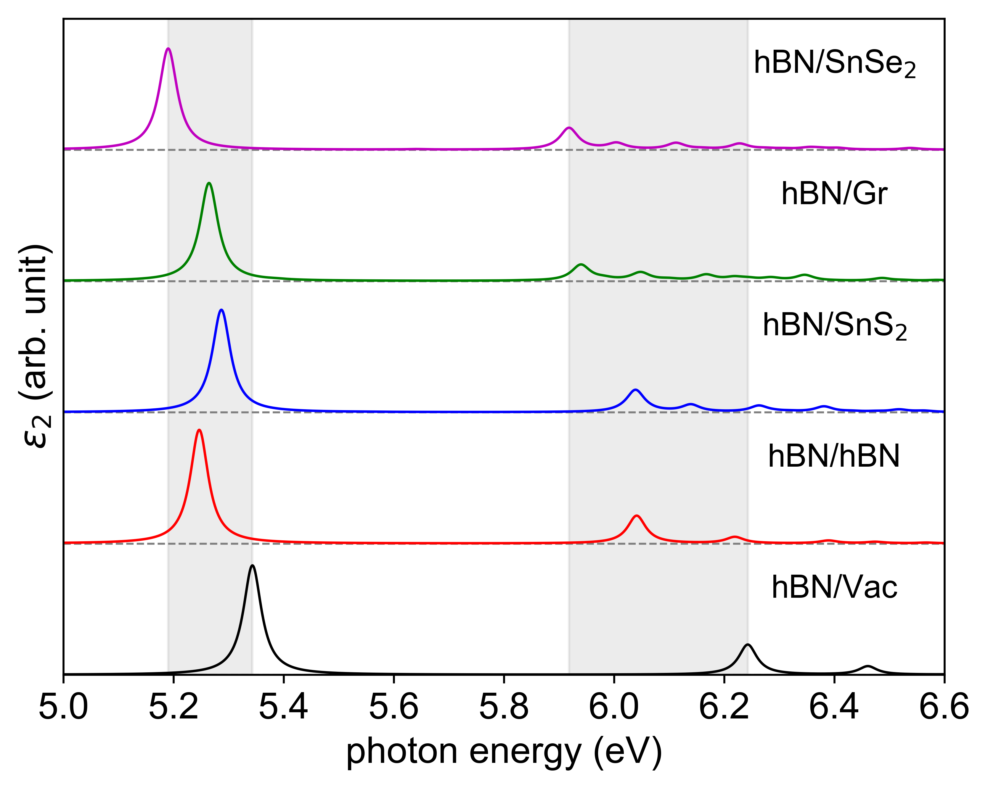
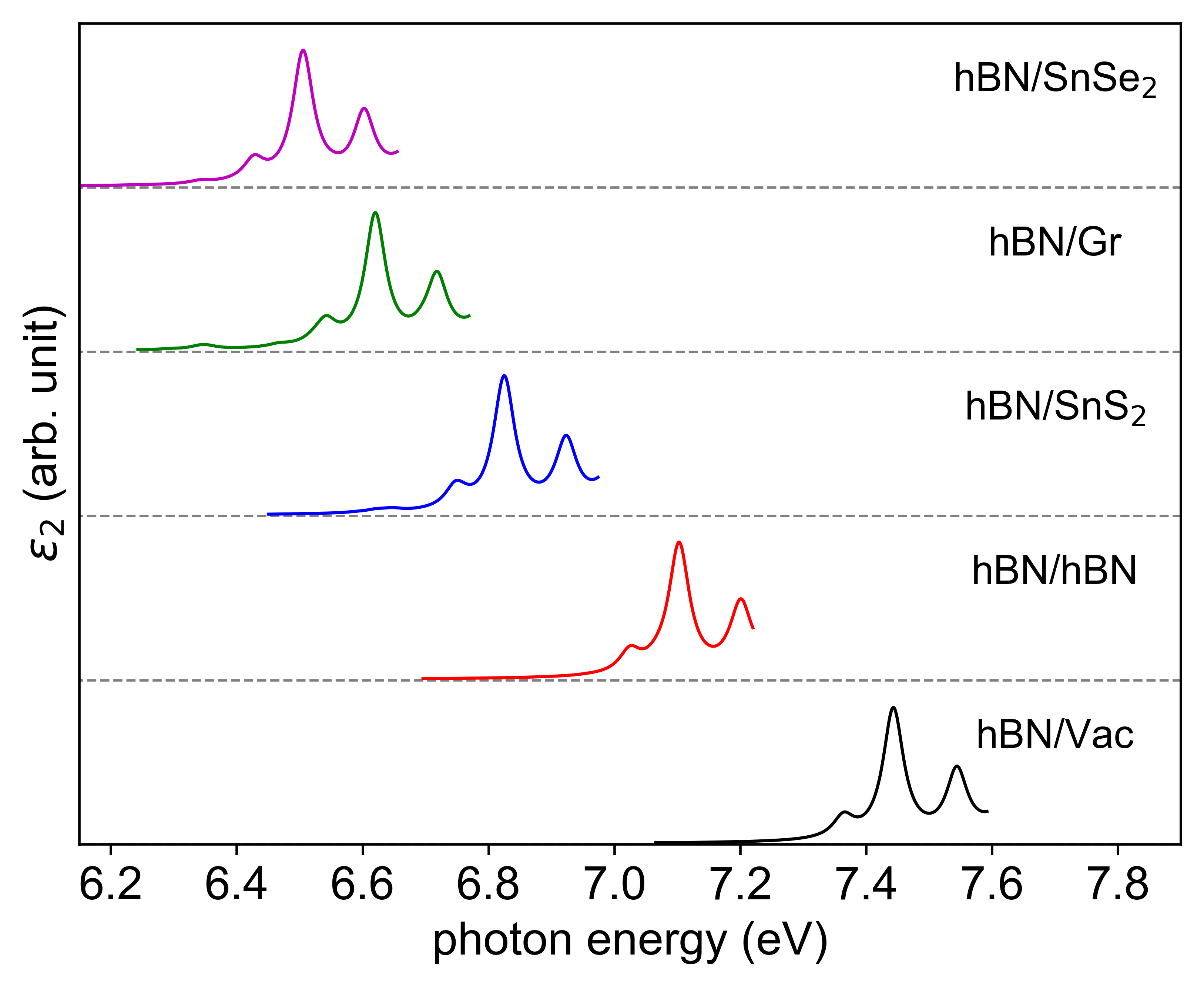
In contrast, Figure 2 shows the RPA spectra of hBN with various substrates using GW quasiparticle energies exhibit a nearly-rigid shift to a lower energy (compared to free-standing hBN). The red shift is mainly due to the reduction of electronic band gap in the presence of substrate screening. This rigid shift may be qualitatively explained by the independence of k-point for electronic band structure under Born approximation Cho and Berkelbach (2018); Waldecker et al. (2019), which has been reported for 2D semiconductors (e.g. WS2) Waldecker et al. (2019).
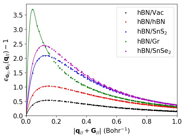
In general, we find the reduction of quasiparticle band gaps due to substrates increases with stronger substrate dielectric screening. However, a simple dielectric constant picture is insufficient to describe low dimensional systems. Specifically, we show the in-plane diagonal elements of dielectric matrices in Figure 3. For example, comparing with the SnSe2 substrate (purple dots), the graphene substrate (green dots) has a stronger dielectric screening at a small momentum transfer region close to zero, and a weaker dielectric screening at a larger momentum transfer region. As a result, the reduction of band gap with the SnSe2 substrate is larger than the one with the graphene substrate although graphene is closer to a metallic system at the Dirac cone than SnSe2. Therefore, fully first principle calculations are required to get reliable prediction of screening effects by various substrates.
III.2 1s and 2s exciton binding energy change with substrate screening
The difference between BSE excitation energies () and electronic band gaps defines exciton binding energy for excitonic state :
| (1) |
We found the proportionality between 1s and 2s exciton binding energies across different substrates falls into a linear relation (i.e. with a slope of 0.73 for ), as shown in Figure 4.
To understand the physical meaning of this linear scaling obtained by solving BSE, we compare our results with the previous 2D hydrogen model of excitons Chernikov et al. (2014); Olsen et al. (2016), which has been used to interpret the exciton energies of free-standing 2D materials. Here we will test the applicability of this model for substrate screening effect on 2D excitons. In this model, we express the 2D dielectric function as , where is the 2D polarizability. The exciton binding energies of th 2D Rydberg-like excitonic state Yang et al. (1991) () can be expressed as:
| (2) |
where is the exciton reduced mass and is the effective dielectric constant for excitonic state, defined as Olsen et al. (2016):
| (3) |
Further simplification Olsen et al. (2016); Jiang et al. (2017) of Eq. 2 with Eq. 3 gives 2D exciton binding energy independent of exciton reduced mass as follows:
| (4) |
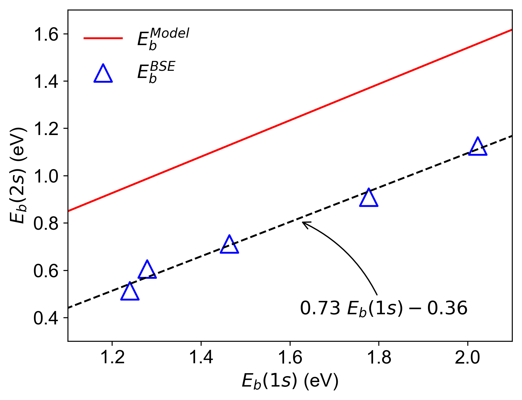
From Eq. 4, we have and . The ratio between and is a constant from this simplified model. Figure 4 shows the linear scaling between 1s and 2s exciton binding energies of monolayer hBN when changing its substrates. The scaling behavior by the model in Eq. 4 (red curve) is in qualitative agreement with our GW/BSE results (blue triangles), i.e. both of which have a linear relation between 2s and 1s exciton binding energies, with a ratio of less than one (Model: 0.78; GW/BSE: 0.73), corresponding to the slope. This implies the change of 1s is larger than the change of 2s due to substrate screening, with a constant ratio while varying the substrate materials. Figure 4 also shows a constant shift between the first-principles scaling and the model one. This discrepancy independent of specific screening environment may come from the limitation of 2D hydrogen model, i.e. either the strict 2D limit of is unrealistic considering the finite thickness of materials, or hBN has tighter-bounded excitons Galvani et al. (2016), deviated from 2D Wannier excitons assumed in previous 2D hydrogen model. Note that the explicit form of Eq. 4 and related linear scaling behavior is based on strict 2D limit of Eq. 2, which is better to describe the interface with relatively small thickness, e.g. heterostructures formed by atomically thin materials. We anticipate that this simplified model may become inappropriate for interface systems with large thickness, especially for systems with high dielectric semi-infinite substrates Riis-Jensen et al. (2020).
III.3 Substrate induced linear scaling relation between and
The exciton peak positions are determined by both the exciton binding energies and electronic band gaps, which have opposite trends while increasing substrate screenings. The relationship between these two quantities was studied for free-standing 2D systems Choi et al. (2015); Jiang et al. (2017), where across a wide range of 2D materials.Yet, no investigation on their relationship when varying substrates has been carried out.
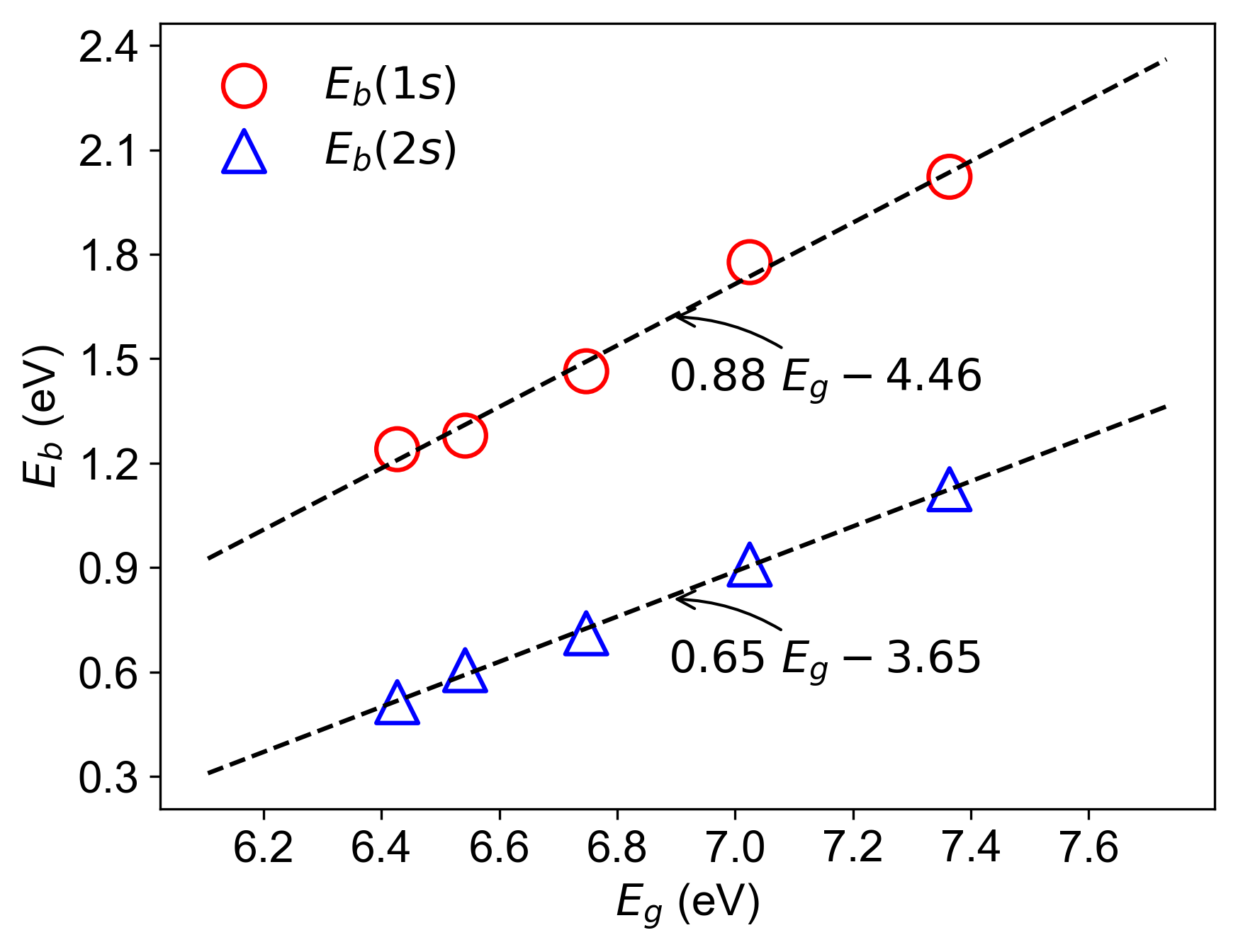
In Figure 5, we show the calculated electronic gap () and exciton binding energy of 1s (red circle) and 2s (blue triangle) () for monolayer hBN at various substrates. Our first-principle results show a linear scaling between exciton binding energy (1s peak position) and quasiparticle electronic band gap due to substrate screening, with a slope nearly close to one (0.88 in Figure 5, linear fitting the computed data (red circles) with a black dashed line). This indicates that the changes of 1s exciton binding energy and electronic gaps due to substrate screening are largely canceled out. Therefore, the first exciton peak (1s) is at a relatively stable position, insensitive to the environmental screening. This explains the experimental and theoretical results in Figures 1 and 6, where the first excitonic peak has rather small shifts with changing environmental screening.
This linear scaling is significantly different from the scaling across different monolayer 2D materials Jiang et al. (2017); Choi et al. (2015). Physically, the scaling between and due to substrate screening has very different nature from the one of free-standing monolayer semiconductor. The environmental screening can be approximately described by classical electrostatic potential of dielectric interface Cho and Berkelbach (2018); Waldecker et al. (2019), which gives a similar reduction on quasi-particle band gaps and exciton binding energies by 2D hydrogen model (linear scaling slope ).
On the other hand, the scaling between 2s binding energy and electronic gap is significantly smaller (0.65) than unity, which indicates the change of 2s exciton binding energy is a lot smaller than the electronic gap with increasing substrate screening. Therefore, the 2s exciton peak position is dominated by the change of electronic gap, which red shifts the spectra with increasing substrate screening (i.e. from vacuum to interfacing with SnSe2 in Figure 6). This stronger red shift of 2s exciton peak than 1s is also expected from the smaller reduction of 2s binding energy with increasing substrate screening in Figure 4.
III.4 Layer dependence of WS2 optical spectra
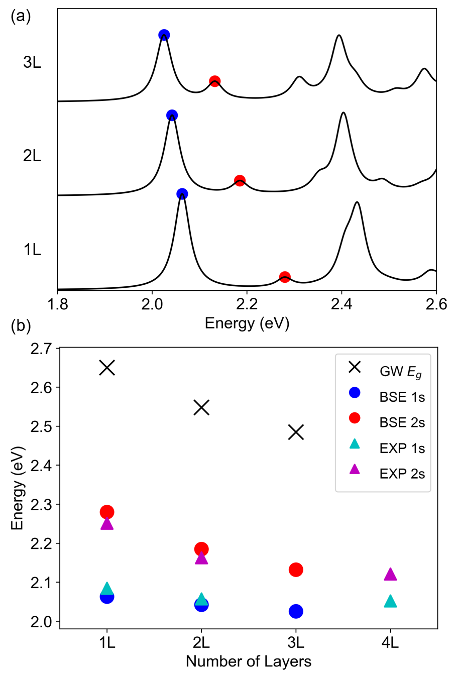
To further validate our method for substrate screenings on optical properties, we calculate the optical spectra from one to three-layer WS2 with the GW/BSE method, then compare with recent experimental results Chernikov et al. (2014). The multi-layer calculations are performed with “-sum” method introduced earlier Guo et al. (2020), which is computationally efficient and properly includes interlayer Coulomb interactions from first-principles.
As shown in Figure 6, we find the position of the first peak (1s, blue dot) is nearly unchanged (shifted within 20 meV) when increasing the number of layers, while the position of the second peak (2s, red dot) shifts over 100 meV. The calculated results with blue (1s) and red dots (2s) are compared with the experimental results (1s, blue triangle) and (2s, purple triangle). From 1L to 4L, the agreements between experiments and theory are nearly perfect, which validate the accuracy of our methods. Meanwhile, the calculated electronic gaps (black cross) are also shown in Figure 6b, with a strong reduction as increasing the number of layers, in sharp contrast to the nearly unchanged optical gaps (1s exciton energies, red dots).
III.5 Exciton lifetime in the presence of substrates
III.5.1 Zero temperature exciton lifetime
Environmental screening due to substrates can also significantly modify the exciton lifetime , which is a critical parameter that determines quantum efficiency. The radiative rate (inverse of lifetime ) based on the Fermi’s Golden rule can be defined as follows Wu et al. (2019b); Palummo et al. (2015):
| (5) |
where denotes the ground-state wavefunction, the excited state, the excitation energy, photon wave-vector, photon polarization direction and exciton wave-vector. Then the radiative decay rate can be defined as the summation of each photon mode:
| (6) |
the corresponding radiative lifetime can be defined as the inverse of rate . Furthermore, the radiative decay rate can be separated into two parts:
| (7) |
where is the exciton decay rate at and has exciton wave-vector dependence. Note that the dependence will be only important to the exciton lifetime at finite temperature Wu et al. (2019b). Therefore the zero-temperature lifetime is simply .
Specifically for two-dimensional exciton lifetime at zero temperature, we have Wu et al. (2019b)
| (8) |
where is the exciton energy, is the unit cell area, and is the module square of dipole matrix elements Wu et al. (2019b).
| Sub | |||
|---|---|---|---|
| Vac | 5.34 | 0.788 | 30.9 |
| hBN | 5.25 | 0.818 | 30.3 |
| SnS2 | 5.29 | 0.738 | 33.3 |
| Gr | 5.26 | 0.706 | 35.0 |
| SnSe2 | 5.19 | 0.729 | 34.3 |
| Sub | |||
|---|---|---|---|
| Vac | 6.24 | 0.218 | 95.6 |
| hBN | 6.04 | 0.201 | 107.1 |
| SnS2 | 6.04 | 0.162 | 132.5 |
| Gr | 5.94 | 0.120 | 182.8 |
| SnSe2 | 5.92 | 0.159 | 138.1 |
The computed and exciton lifetimes of monolayer hBN on various substrates at zero temperature are shown in Table 1 and Table 2 respectively. The effect of substrate screening on comes from the quench of oscillator strength (or dipole moment ) and the red-shift of exciton energy, both of which increase the lifetime. In Table 1 and 2, are reduced by a similar amount between 1s and 2s excitons with increasing substrate screening; however, the relative proportion of reduction is much larger in 2s exciton due to its much weaker than 1s exciton. This results in stronger increase in 2s exciton lifetime (i.e. increased by fs) in Table 2. Instead, exciton lifetime is rather insensitive to the substrate screening in Table 1.
III.5.2 Finite temperature exciton lifetime
The radiative exciton decay rate at finite temperature can be calculated by the thermal average of all accessable excitonic states as follows:
| (9) | ||||
| (10) |
where is the exciton energy dispersion as a function of exciton wave-vector . Since a constant shift of does not change the expression of rate , we will use to replace in all later discussions, where is the lowest exciton energy. As the integration of Eqs. 9-10 requires the dispersion of exciton energy , we use the effective mass approximation for exciton energy dispersion.
| Mat | |||
|---|---|---|---|
| ML WS2 | 334 | 923 | 806 Yuan and Huang (2015) |
| Sub | ||
|---|---|---|
| Vac | 30.9 | 33.3 |
| hBN | 30.3 | 32.6 |
| SnS2 | 33.3 | 35.8 |
| Gr | 35.0 | 37.7 |
| SnS2 | 34.3 | 37.0 |
First, we compute the room temperature (300K) exciton radiative lifetime of monolayer (ML) WS2 to compare with experimental lifetime Yuan and Huang (2015). The effective mass approximation for exciton dispersion is defined as , where is the exciton effective mass. is chosen to be the summation of electron and hole effective mass, which was shown adequate for Wannier excitons Mattis and Gallinar (1984). The electron () and hole () effective mass are from GW band structure results Shi et al. (2013) (). Our calculated lifetime at room temperature is 923 ps for monolayer WS2, in excellent agreement with experimental lifetime 806 ps Yuan and Huang (2015) as shown in Table 3.
We then apply the same methodology to compute the exciton radiative lifetime for monolayer hBN with various substrates at finite temperature, as shown in Table 4. We find within the effective mass approximation, the room temperature exciton lifetime is much longer ( orders) than the zero temperature lifetime . To confirm the exciton lifetime of monolayer hBN with substrates in Table 4 at finite temperature, future experimental work will be necessary.
IV Conclusion
In this work we examined the substrate screening effects on excitonic excitation and recombination lifetime of 2D materials. We applied our previously developed effective polarizablility (-sum) method to efficiently calculate the electronic and optical spectra for arbitrary 2D interfaces with GW method and solving the BSE. We revealed the underlying mechanism of the non-rigid shifts of 1s and 2s peaks, i.e. why 2s red shifts much stronger than 1s in the presence of substrate screening. We explained this phenomenon through two steps: first, we showed a linear scaling (with a ratio of less than one) between 1s and 2s exciton binding energy both from our first-principle results and 2D Wannier exciton models; second, we presented the linear scaling between electronic gaps and exciton binding energies with a slope close to 1 for 1s and much smaller for 2s exciton while varying substrate screening. We further validated our method by reproducing the 1s and 2s exciton energy shift of WS2 as a function of layer thickness observed experimentally. Finally we investigated the substrate effects on exciton lifetime and found the 2s exciton lifetime has a stronger dependence on substrates than 1s, due to the relative large change of exciton dipole moment.
Acknowledgements
This work is supported by National Science Foundation under grant No. DMR-1760260 and DMR-1956015. This research used resources of the Center for Functional Nanomaterials, which is a US DOE Office of Science Facility, and the Scientific Data and Computing center, a component of the Computational Science Initiative, at Brookhaven National Laboratory under Contract No. DE-SC0012704, the lux supercomputer at UC Santa Cruz, funded by NSF MRI grant AST 1828315, the National Energy Research Scientific Computing Center (NERSC) a U.S. Department of Energy Office of Science User Facility operated under Contract No. DE-AC02-05CH11231, the Extreme Science and Engineering Discovery Environment (XSEDE) which is supported by National Science Foundation Grant No. ACI-1548562 (Towns et al., 2014).
References
- Chernikov et al. (2014) A. Chernikov, T. C. Berkelbach, H. M. Hill, A. Rigosi, Y. Li, O. B. Aslan, D. R. Reichman, M. S. Hybertsen, and T. F. Heinz, Physical Review Letters 113, 076802 (2014).
- Qiu et al. (2013) D. Y. Qiu, H. Felipe, and S. G. Louie, Physical Review Letters 111, 216805 (2013).
- Wolf et al. (2001) S. Wolf, D. Awschalom, R. Buhrman, J. Daughton, v. S. von Molnár, M. Roukes, A. Y. Chtchelkanova, and D. Treger, Science 294, 1488 (2001).
- Žutić et al. (2004) I. Žutić, J. Fabian, and S. D. Sarma, Reviews of Modern Physics 76, 323 (2004).
- He et al. (2015) Y.-M. He, G. Clark, J. R. Schaibley, Y. He, M.-C. Chen, Y.-J. Wei, X. Ding, Q. Zhang, W. Yao, X. Xu, et al., Nature Nanotechnology 10, 497 (2015).
- Tran et al. (2016a) T. T. Tran, K. Bray, M. J. Ford, M. Toth, and I. Aharonovich, Nature Nanotechnology 11, 37 (2016a).
- Novoselov et al. (2016) K. Novoselov, A. Mishchenko, A. Carvalho, and A. C. Neto, Science 353, aac9439 (2016).
- Winther and Thygesen (2017) K. T. Winther and K. S. Thygesen, 2D Materials 4, 025059 (2017).
- Ugeda et al. (2014) M. M. Ugeda, A. J. Bradley, S.-F. Shi, H. Felipe, Y. Zhang, D. Y. Qiu, W. Ruan, S.-K. Mo, Z. Hussain, Z.-X. Shen, et al., Nature Materials 13, 1091 (2014).
- Waldecker et al. (2019) L. Waldecker, A. Raja, M. Rösner, C. Steinke, A. Bostwick, R. J. Koch, C. Jozwiak, T. Taniguchi, K. Watanabe, E. Rotenberg, et al., Physical Review Letters 123, 206403 (2019).
- Raja et al. (2017) A. Raja, A. Chaves, J. Yu, G. Arefe, H. M. Hill, A. F. Rigosi, T. C. Berkelbach, P. Nagler, C. Schüller, T. Korn, et al., Nature Communications 8, 1 (2017).
- Ping et al. (2013) Y. Ping, D. Rocca, and G. Galli, Chem. Soc. Rev. 42, 2437 (2013).
- Guo et al. (2020) C. Guo, J. Xu, D. Rocca, and Y. Ping, Physical Review B 102, 205113 (2020).
- Olsen et al. (2016) T. Olsen, S. Latini, F. Rasmussen, and K. S. Thygesen, Physical Review Letters 116, 056401 (2016).
- Choi et al. (2015) J.-H. Choi, P. Cui, H. Lan, and Z. Zhang, Physical Review Letters 115, 066403 (2015).
- Jiang et al. (2017) Z. Jiang, Z. Liu, Y. Li, and W. Duan, Physical Review Letters 118, 266401 (2017).
- Cho and Berkelbach (2018) Y. Cho and T. C. Berkelbach, Physical Review B 97, 041409 (2018).
- Perdew et al. (1996) J. P. Perdew, K. Burke, and M. Ernzerhof, Physical Review Letters 77, 3865 (1996).
- Giannozzi et al. (2017) P. Giannozzi, O. Andreussi, T. Brumme, O. Bunau, M. B. Nardelli, M. Calandra, R. Car, C. Cavazzoni, D. Ceresoli, M. Cococcioni, N. Colonna, I. Carnimeo, A. D. Corso, S. de Gironcoli, P. Delugas, R. A. DiStasio, A. Ferretti, A. Floris, G. Fratesi, G. Fugallo, R. Gebauer, U. Gerstmann, F. Giustino, T. Gorni, J. Jia, M. Kawamura, H.-Y. Ko, A. Kokalj, E. Küçükbenli, M. Lazzeri, M. Marsili, N. Marzari, F. Mauri, N. L. Nguyen, H.-V. Nguyen, A. O. de-la Roza, L. Paulatto, S. Poncé, D. Rocca, R. Sabatini, B. Santra, M. Schlipf, A. P. Seitsonen, A. Smogunov, I. Timrov, T. Thonhauser, P. Umari, N. Vast, X. Wu, and S. Baroni, Journal of Physics: Condensed Matter 29, 465901 (2017).
- Hamann (2013) D. Hamann, Physical Review B 88, 085117 (2013).
- Grimme (2006) S. Grimme, Journal of Computational Chemistry 27, 1787 (2006).
- Barone et al. (2009) V. Barone, M. Casarin, D. Forrer, M. Pavone, M. Sambi, and A. Vittadini, Journal of Computational Chemistry 30, 934 (2009).
- Marini et al. (2009) A. Marini, C. Hogan, M. Grüning, and D. Varsano, Computer Physics Communications 180, 1392 (2009).
- Yan et al. (2011) J. Yan, K. S. Thygesen, and K. W. Jacobsen, Physical Review Letters 106, 146803 (2011).
- Rozzi et al. (2006) C. A. Rozzi, D. Varsano, A. Marini, E. K. U. Gross, and A. Rubio, Phys. Rev. B 73, 205119 (2006).
- Mendelson et al. (2020) N. Mendelson, D. Chugh, J. R. Reimers, T. S. Cheng, A. Gottscholl, H. Long, C. J. Mellor, A. Zettl, V. Dyakonov, P. H. Beton, S. V. Novikov, C. Jagadish, H. H. Tan, M. J. Ford, M. Toth, C. Bradac, and I. Aharonovich, Nature Materials (2020).
- Tran et al. (2016b) T. T. Tran, K. Bray, M. J. Ford, M. Toth, and I. Aharonovich, Nature Nanotechnology 11, 37 (2016b).
- Gottscholl et al. (2020) A. Gottscholl, M. Kianinia, V. Soltamov, S. Orlinskii, G. Mamin, C. Bradac, C. Kasper, K. Krambrock, A. Sperlich, M. Toth, I. Aharonovich, and V. Dyakonov, Nature Materials 19, 540 (2020).
- Turiansky et al. (2020) M. E. Turiansky, A. Alkauskas, and C. G. Van de Walle, Nature Materials 19, 487 (2020).
- Wu et al. (2019a) F. Wu, T. J. Smart, J. Xu, and Y. Ping, Physical Review B 100, 081407 (2019a).
- Smart et al. (2018) T. J. Smart, F. Wu, M. Govoni, and Y. Ping, Physical Review Materials 2, 124002 (2018).
- Wu et al. (2017) F. Wu, A. Galatas, R. Sundararaman, D. Rocca, and Y. Ping, Physical Review Materials 1, 071001 (2017).
- Smart et al. (2020) T. J. Smart, K. Li, J. Xu, and Y. Ping, arXiv preprint arXiv:2009.02830 (2020).
- Sajid et al. (2020) A. Sajid, M. J. Ford, and J. R. Reimers, Reports on Progress in Physics 83, 044501 (2020).
- Yang et al. (1991) X. Yang, S. Guo, F. Chan, K. Wong, and W. Ching, Physical Review A 43, 1186 (1991).
- Galvani et al. (2016) T. Galvani, F. Paleari, H. P. Miranda, A. Molina-Sánchez, L. Wirtz, S. Latil, H. Amara, and F. Ducastelle, Physical Review B 94, 125303 (2016).
- Riis-Jensen et al. (2020) A. C. Riis-Jensen, M. N. Gjerding, S. Russo, and K. S. Thygesen, Physical Review B 102, 201402 (2020).
- Wu et al. (2019b) F. Wu, D. Rocca, and Y. Ping, Journal of Materials Chemistry C 7, 12891 (2019b).
- Palummo et al. (2015) M. Palummo, M. Bernardi, and J. C. Grossman, Nano Letters 15, 2794 (2015).
- Yuan and Huang (2015) L. Yuan and L. Huang, Nanoscale 7, 7402 (2015).
- Shi et al. (2013) H. Shi, H. Pan, Y.-W. Zhang, and B. I. Yakobson, Physical Review B 87, 155304 (2013).
- Mattis and Gallinar (1984) D. Mattis and J.-P. Gallinar, Physical Review Letters 53, 1391 (1984).
- Towns et al. (2014) J. Towns, T. Cockerill, M. Dahan, I. Foster, K. Gaither, A. Grimshaw, V. Hazlewood, S. Lathrop, D. Lifka, G. D. Peterson, R. Roskies, J. R. Scott, and N. Wilkins-Diehr, Comput. Sci. Eng. 16, 62 (2014).