Design Of Two Stage CMOS Operational Amplifier in 180nm Technology
Abstract
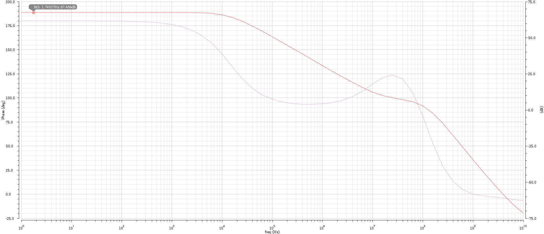
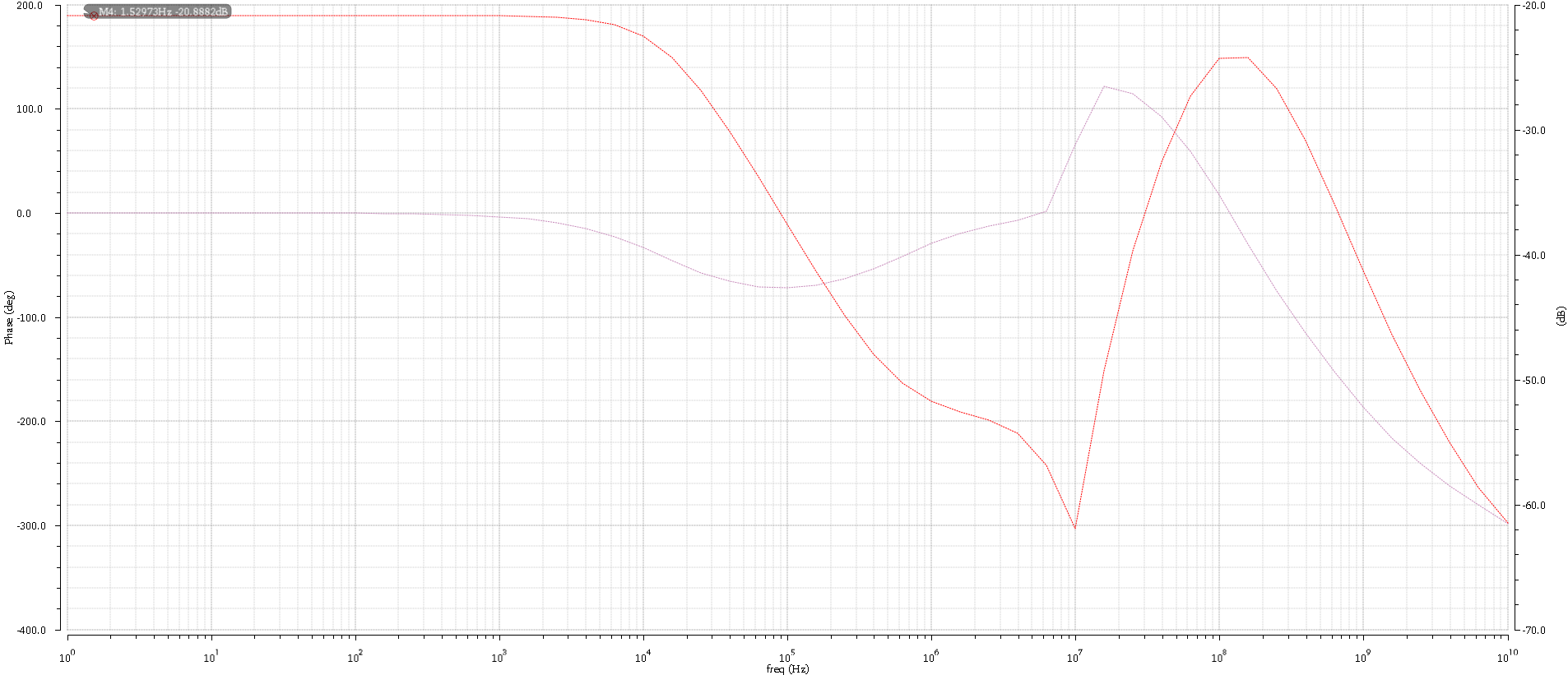
In this paper a CMOS two stage operational amplifier has been presented which operates at 1.8 V power supply at 0.18 micron (i.e., 180 nm) technology and whose input is depended on Bias Current. The op-amp provides a gain of 63dB and a bandwidth of 140 kHz for a load of 1 pF. This op-amp has a Common Mode gain of -25 dB, an output slew rate of 32 , and a output voltage swing. The power consumption for the op-amp is .
Index Terms:
Phase Margin, Gain Bandwidth Product, CMRR, ICMR, CMOS Analog circuit.I Introduction
The trend towards low voltage low power silicon chip systems has been growing due to the increasing demand of smaller size and longer battery life for portable applications in all marketing segments including telecommunications, medical, computers and consumer electronics. The operational amplifier is undoubtedly one of the most useful devices in analog electronic circuitry. Op-amps are built with different levels of complexity to be used to realize functions ranging from a simple dc bias generation to high speed amplifications or filtering. With only a handful of external components, it can perform a wide variety of analog signal processing tasks. Op-amps are among the most widely used electronic devices today, being used in a vast array of consumer, industrial, and scientific devices. Operational Amplifiers, more commonly known as Op-amps, are among the most widely used building blocks in Analog Electronic Circuits.
Op-amps are linear devices which has nearly all the properties required for not only ideal DC amplification but is used extensively for signal conditioning, filtering and for performing mathematical operations such as addition, subtraction, integration, differentiation etc . Generally an Operational Amplifier is a 3-terminal device.It consists mainly of an Inverting input denoted by a negative sign, (”-”) and the other a Non-inverting input denoted by a positive sign (”+”) in the symbol for op-amp. Both these inputs are very high impedance. The output signal of an Operational Amplifier is the magnified difference between the two input signals or in other words the amplified differential input. Generally the input stage of an Operational Amplifier is often a differential amplifier.
An operational amplifier is a DC-coupled differential input voltage amplifier with an rather high gain. In most general purpose op-amps there is a single ended output. Usually an op-amp produces an output voltage a million times larger than the voltage difference across its two input terminals. For most general applications of an opamp a negative feedback is used to control the large voltage gain. The negative feedback also largely determines the magnitude of its output (”closed- loop”) voltage gain in numerous amplifier applications, or the transfer function required. The op-amp acts as a comparator when used without negative feedback, and even in certain applications with positive feedback for regeneration. An ideal Opamp is characterized by a very high input impedance (ideally infinite) and low output impedance at the output terminal(s) (ideally zero).to put it simply the op- amp is one type of differential amplifier. This section briefly discusses the basic concept of op-amp. An amplifier with the general characteristics of very high voltage gain, very high input resistance, and very low output resistance generally is referred to as an op-amp. Most analog applications use an Op-Amp that has some amount of negative feedback. The Negative feedback is used to tell the Op-Amp how much to amplify a signal. And since op-amps are so extensively used to implement a feedback system, the required precision of the closed loop circuit determines the open loop gain of the system.
II Theoretical Analysis
II-A MOSFET ans Two Stage amp
For MOSFET we have several basic parameters including
and
for calculation, we have parameters and
II-B Gain, Pole and zeros
We define the input , the output voltage of the first stage i.e. the input voltage of the second stage , and the output voltage of the whole circuit , so we can get that for two stage operational amplifier we have
so we can calculate the voltage gain of two stage separately and then combine together.
We set the output resistance of the first stage as and the output resistance of the second stage as . We also se the output capacitance of the first stage as and for the second stage. So we finally get that
with
and
to find the poles and zeros, we must transform the equation into form like
here for this two stage amplifier we have the DC gain of the amplifier
the zero point of the circuit
, and with a external resistor,
so we could set
When it comes to the poles of the circiut, approximately we have
we can simply it to
for another pole we have
is very small so we can simply it into
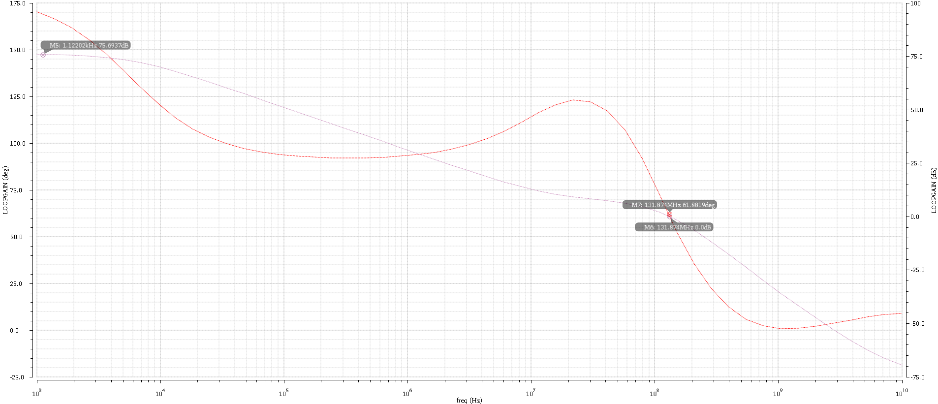
II-C Phase Margin
The gain band with GBW is equal to
For phase margin, we have
and we have
by substituting
so
then we need
and finally
to get more than phase margin. Thus we also have
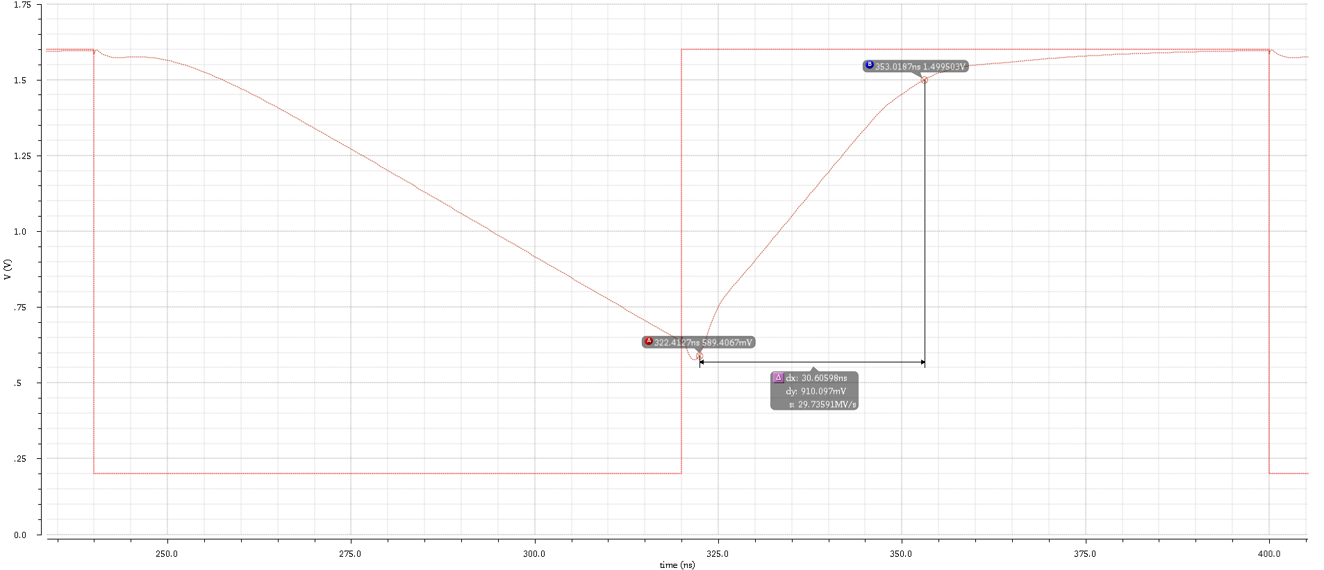
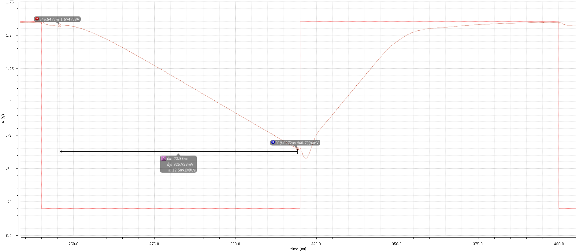
II-D Slew Rate
In our design, the slew rate is just equal to
we already have so must be under 10C, with is certain to full-fill. Here we need to obtain slew rate under 100MHZ, so we need the voltage change more than 0.05V in one pulse, which is 5ns in width.
II-E Power
The power of the op-amp can be calculated by
III Design Procedure
III-A Design Goal
| Parameters | Design Goal |
|---|---|
| Process | 0.18µm CMOS |
| 1.8V | |
| 0V | |
| Load | 1pF |
| Phase margin | |
| (60dB) | |
| (-20dB) | |
| Unity gain frequency | |
| Slew rate | |
| Output voltage swing (differential peak to peak) | |
| Power | Minimum |
Bonus: Design your opamp such that the specifications are met under a ±10% variation of the supply voltage.
III-B Design Principle
The minimum size of the MOSFET we can use is 180nm in length and 400 nm in width, but normally we don’t use the minimum channel length due to the increase of the . is recommended, in this design, we use . And after initially designed, to optimise the performance of the op-amp, we will adjust the length of some MOSFET while keep the (W/L) unchanged.
To control the systematic offset we set
We also have
and
During the procedure of the design. we first calculate the proper value of the compensate capacitance and resistance, then we will design the first stage, finally the second stage will be designed.
III-C Parameter Optimization
III-C1 Design of
To satisfy the phase margin of we need , since we have so we can use . To achieve slew rate we need , to meet a balance between two requirement, and we choose
III-C2 Design of M1 and M2
We have
and GBW is also called unity gain frequency, which is listed in the design goal with value of 100MHZ. So we need to apply that
and for convince we choose a litter larger value . Since
and , fianly we get
so we use 20 as the final value of the ratio.
III-C3 Design of M3 and M4
To get more than 800mV of the output range, we need to at least 800mV input common mode voltage range before the zero point, where the gain is 1. This characteristic parameter can also be used to determined the size of the MOSFET M1 and M2. We have
we choose ICMR(+) at 1.6V and we get .
III-C4 Design of M5 and M8
In the mean while, we also need to fit the proper value of ICMR(-) to determine the size of MOSFET M5. We have
with
Approximately we can choose and
III-C5 Design of M6
And also we need , so we need , we want
and
So we need
so here we get
III-C6 Design of M7
III-C7 Design of
III-C8 Common and differential mode gain
After initially determining the parameters of the MOSFETs, we need to check output voltage gain, than we may need to adjust the parameters to meet the requirements of common and differential mode voltage gain.
IV Our design
After we initially determine the parameters, we use Parameter Analysis in Cadence Virtuoso to optimize our design and finall we get the design as shown in Table II, and the simulation results are in Table III.
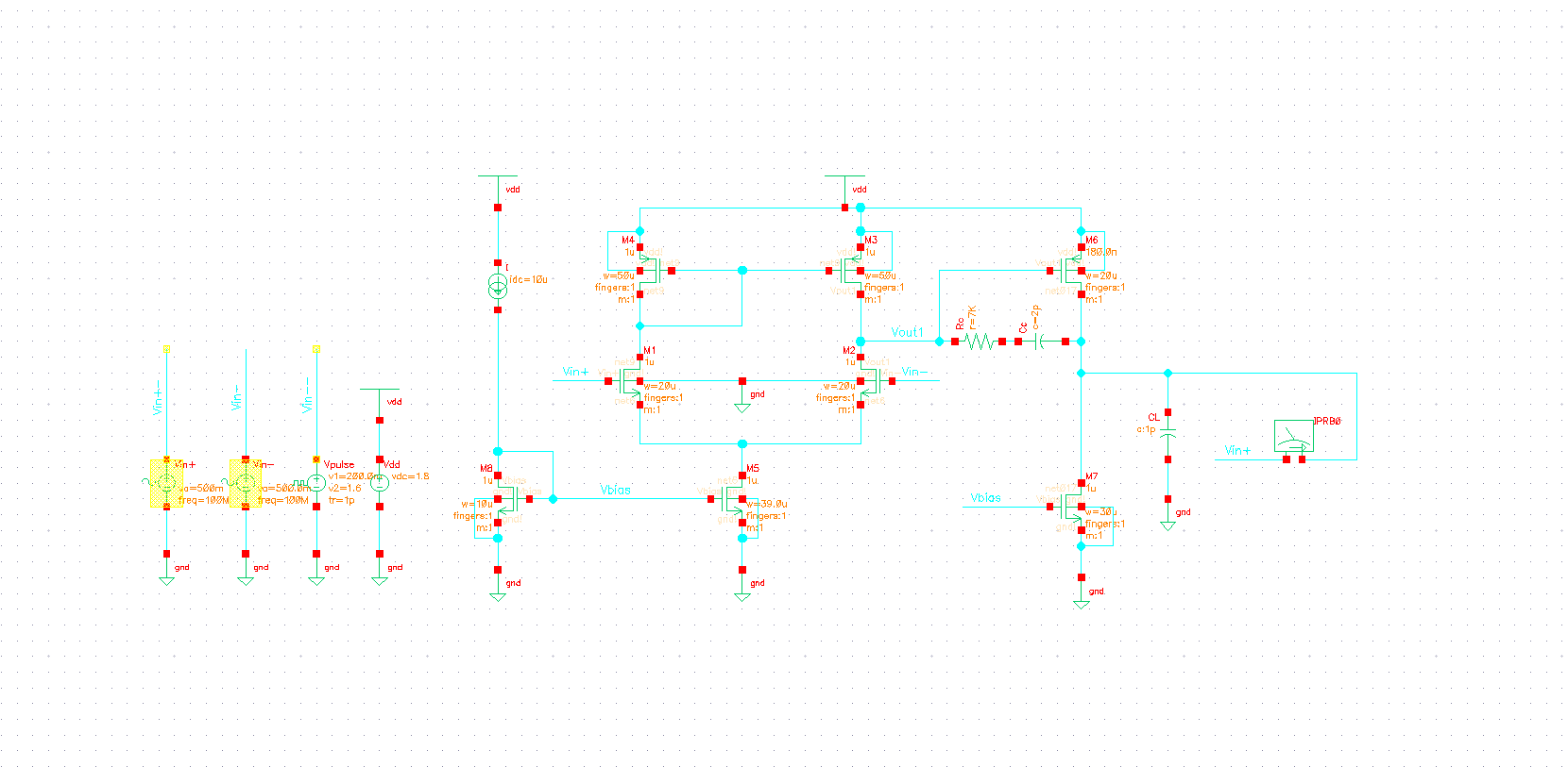
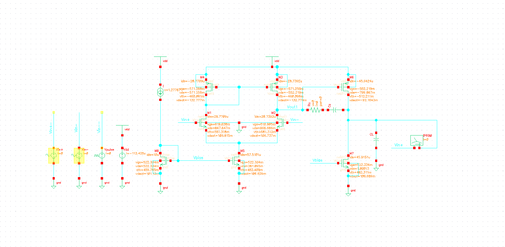
The final design schematic is named project-final
| Device | Length (L) | Width (W) | W/L |
|---|---|---|---|
| M1 | 1u | 20u | 20 |
| M2 | 1u | 20u | 20 |
| M3 | 1u | 50u | 50 |
| M4 | 1u | 50u | 50 |
| M5 | 1u | 39u | 39 |
| M6 | 180n | 20u | 111 |
| M7 | 1u | 30u | 30 |
| M8 | 1u | 10u | 10 |
| Parameter | Design |
|---|---|
| 2pF | |
| I | 10uA |
V Conclusion
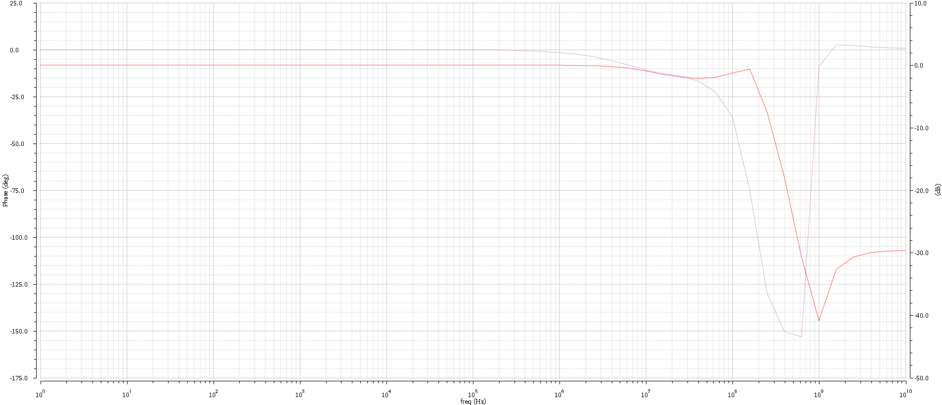
In this design, we have satisfied all the parameters in the requirement and specially we achieved high , slew rate and wide unity gain phase margin. By comparison we found that the simulation result is a little different from out theoretical design due to some omitting during our calculation. But after all, our calculation has represent the real situation and offered great help in the design of the device.
VI Appendix
References
- [1] T. H. Kim, “6.012 DP: CMOS Integrated Differential Amplifier,” p. 9.
- [2] R. Sotner, J. Jerabek, R. Prokop, V. Kledrowetz, and J. Polak, “A CMOS Multiplied Input Differential Difference Amplifier: A New Active Device and Its Applications,” Applied Sciences, vol. 7, no. 1, p. 106, Jan. 2017, doi: 10.3390/app7010106.
- [3] A. R. A. El-mon’m and A. W. Abdallah, “CMOS Two-Stage Amplifier Design Approach,” p. 5.
- [4] M. H. Hamzah, A. B. Jambek, and U. Hashim, “Design and analysis of a two-stage CMOS op-amp using Silterra’s 0.13 um technology,” in 2014 IEEE Symposium on Computer Applications and Industrial Electronics (ISCAIE), Penang, Malaysia, Apr. 2014, pp. 55–59, doi: 10.1109/ISCAIE.2014.7010209.
- [5] Shu-Chuan Huang and M. Ismail, “Design of a CMOS differential difference amplifier and its applications in A/D and D/A converters,” in Proceedings of APCCAS’94 - 1994 Asia Pacific Conference on Circuits and Systems, Dec. 1994, pp. 478–483, doi: 10.1109/APCCAS.1994.514597.
- [6] S. Bandyopadhyay, D. Mukherjee, and R. Chatterjee, “Design Of Two Stage CMOS Operational Amplifier in 180nm Technology With Low Power and High CMRR,” p. 9.
- [7] H. Ma, G. H. Nam-Goong, S. Kim, S.-I. Lim, and F. Bien, “Differential Difference Amplifier based Parametric Measurement Unit with Digital Calibration,” JSTS, vol. 18, no. 4, pp. 438–444, Aug. 2018, doi: 10.5573/JSTS.2018.18.4.438.