Efficient partitioning of surface Green’s function: toward ab initio contact resistance study.
Abstract
In this work, we propose an efficient computational scheme for first-principle quantum transport simulations to evaluate the open-boundary conditions. Its partitioning differentiates from conventional methods in that the contact self-energy matrices are constructed on smaller building blocks, principal layers (PL), while conventionally it was restricted to have the same lateral dimensions of the adjoining atoms in a channel region. Here, we obtain the properties of bulk electrodes through non-equilibrium Green’s function (NEGF) approach with significant improvements in the computational efficiency without sacrificing the accuracy of results. To exemplify the merits of the proposed method we investigate the carrier density dependency of contact resistances in silicon nanowire devices connected to bulk metallic contacts.
I INTRODUCTION
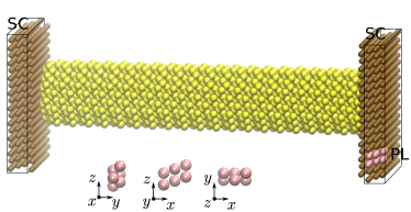
In recent years, quasi one-dimensional (1D) materials such as nanowires and nanotubes have been at the forefront of nanotechnology research. Their unique electronic properties make them promising candidates as next-generation logic switches. However their performance, is often limited by their high contact resistance [1]. First-principles quantum transport simulations are ideally suited to design contacts with low resistances based on atomistic models as close as possible to reality. Such ab initio investigations require heavy computational burden as compared to, e.g., tight-binding or kp models. One of the major bottlenecks arises from calculating the boundary conditions. Usually, the electrodes employed in 1D devices are bulk like, i.e. they consist of a repeating unit cell. The standard method in transport calculations is to build a supercell (SC)-sized contact which is constraint to have at least the same lateral dimensions as the channel (see Fig. 1). Because the computational cost to evaluate the boundary self-energies is in general proportional to the cube of the system size, large-scale electron-transport characterization are often impractical.
In this work, we propose an efficient algorithm to address this issue, partitioning the contact self-energy into smaller building blocks called principal layers (PL). This method allows to fully retain the electronic information of the contacts, while significantly improving the computational efficiency, on the basis of Bloch’s theorem. As an application, we demonstrate the strength of the proposed approach for large-scale quantum transport simulations of silicon nanowires with metallic electrodes and report the resulting contact resistances as a function of the nanowire diameters and carrier densities.
II ALGORITHM
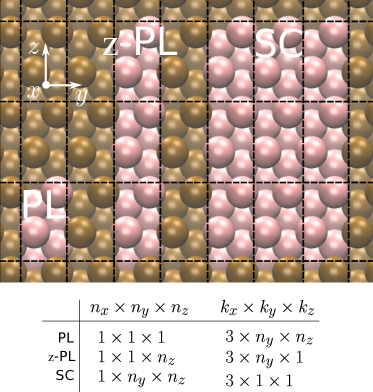
Our self-energy partitioning algorithm is summarized in Fig. 2. We consider a SC contact as a stack of principal layers (PLs) that are repeated times along the - and -directions transverse to the transport -direction. We assume that: i) the PL has only nearest neighbor couplings () in the -direction, with and being odd numbers; ii) the SC is periodic in the - and -directions. First, the electronic structure of the periodic PL is computed with a local basis set of orbitals. The Brillouin zone is sampled with a k-space grid. This ensures that projecting the SC into the PL leads to the corresponding Bloch-space Hamiltonian. We then carry out a partial Bloch sum over the 3 wavevectors in the -direction,
| (1) |
| (2) |
where includes the transverse components ( and ) of . The are the -dependent Hamiltonian matrices. The overlap matrices and are obtained in the same way. Eqs. (1) and (2) transform a set of fully-delocalized Bloch wavefunctions into a set of hybrid wave-functions which remain extended (Bloch-like) along the transverse directions, but are localized in the transport direction. We note that the aforementioned transformation enables the usage of an iterative scheme [2] to compute the surface Green’s function . Hereafter, we drop the energy dependence for ease of readability. By performing a Bloch summation over the transverse wavevectors, the distance-dependent Green’s functions can be finally obtained as
| (3) |
where refer to the position of the PL within the SC. The surface Green’s function within one PL is simply given by . As last step, we construct the SC Green’s function as the circulant matrix
| (4) |
with matrix elements that are themselves circulant
| (5) |
The indices of the first row in and are: and , respectively. The boundary self-energies can then be derived from the matrix products [3]
| (6) |
where with a small positive number while and are the Hamiltonian and overlap matrices, respectively, connecting two consecutive SC in the -direction. They are evaluated in the same way as from the elements of Eq. (2).
Here we highlight the computational efficiency of the proposed algorithm. Indeed, the iterative scheme to compute the surface Green’s function requires to calculate the inverse of a matrix with the same dimensions as . The computational cost is then , where and is the number of basis functions in one PL. Thanks to the proposed partitioning, the computational complexity of the recursive algorithm is reduced to as one has to invert distance-dependent Green’s functions , each of dimension . This scheme is therefore particularly advantageous to simulate 1D devices with large channels. We also note that it is the odd condition on and that ensures a correct inclusion of the minimum-image convention. Careful attention must be payed when constructing the SC contacts which must be able to be partitioned into an odd number of PLs. As an alternative, one can consider a stack of PLs as the smallest building block for which the distant-dependent Green’s functions are evaluated. This is the case when either or is an even number.
III RESULTS
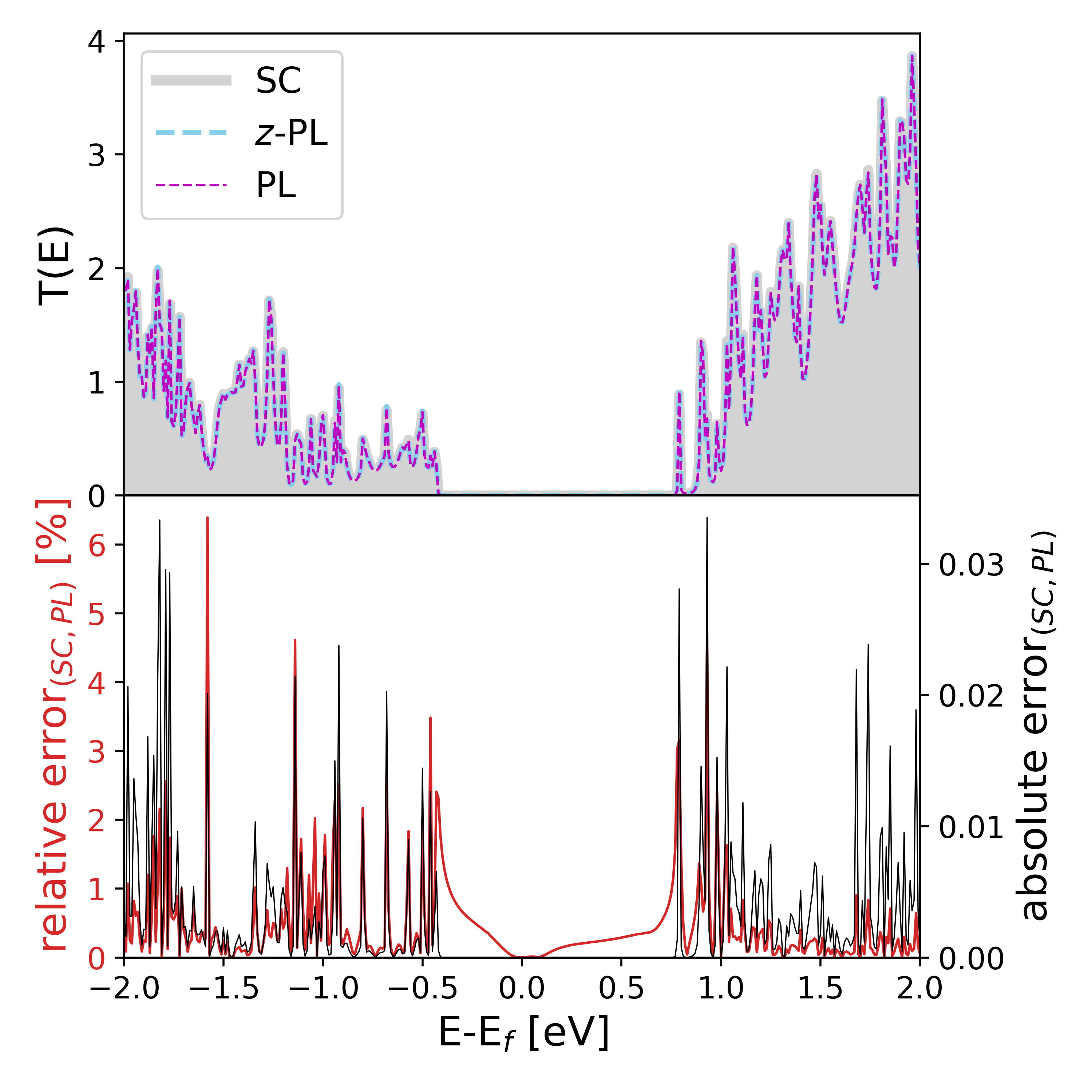
As benchmark example, we consider a Silicon nanowire (SiNW) attached to bulk Au(111) surfaces [4]. The SC are modeled by a three-layer-thick Au(111) and are composed of PLs, each having atoms with orbitals per atom. The scattering region includes the nanowire extended to each terminal with four Au(111) slabs (see Fig. 1). The and matrices are computed from density functional theory (DFT) with GPAW [5] using single zeta polarized (SZP) basis functions and the Perdew, Burke, Ernzerhof (PBE) exchange-correlation functional. To validate the accuracy of our approach, we compare the conductance spectra obtained with the entire SC, a stack of PLs with (-PL), and a single PL. Fig. 3 shows that the proposed algorithm successfully reproduces the SC conductance spectra within absolute errors.
To investigate the influence of the discrepancy in electronic structure results on the conductance spectra, we compare the and matrices obtained by the SC and PL approaches. For the former, the matrices are directly obtained by Eqs. (1) and (2) since the wavefunctions are already real in the transverse directions, whereas for the latter, they are constructed following the same steps outlined for Eqs. (1) to (5). Figs. 4(a-b) report the absolute errors for each entry of the matrices.
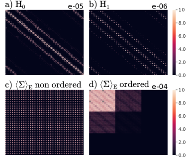
As expected, the large errors appear in the entries connecting neighboring PLs and are comparable with the average absolute error in conductance (see black line in the bottom panel of Fig. 3). We conclude that it is already at the DFT level that the majority of the errors are accumulated. When constructing with Eqs. (4) and (5) we assume that the electronic potential in the PLs is incommensurate with the SC structure, i.e., the diagonal entries and are equivalent. However, the Hamiltonian of the SC does not reflect this symmetry.
To see how the discrepancies introduced by the DFT calculation propagate in the recursive algorithm for computing the surface Green’s function, we evaluate the absolute error between the boundary self-energies obtained with the Hamiltonian and overlap matrices corresponding to the PL and SC structures. To achieve this without loss of generality for energy points, we compute the average error for each entry in using energy points in the range from eV to eV with a regular grid spacing of eV. The result is illustrated in Fig. 4(c) where it can be observed that the absolute error overall increases by one order of magnitude when compared to Figs. 4(a-b). This is attributed to the average number of iterations required to converge , which is found to be . The error adds up linearly at each iteration step. To gain further insights into the distribution of the error, we reorder the matrix elements from Fig. 4(c) so that the atoms in the SC structure are aligned along the transport direction 111The reordering is applied consistently in the conductance calculations where the adjoining atoms in the scattering region are ordered for increasing -coordinate so as to maintain a block tridiagonal structure of the scattering Hamiltonian [6].. The resulting matrix is plotted in Fig. 4(d). It can be seen that the majority of the errors appear in the entries in the upper-left corner which couples the electrodes to the adjoining atoms in the scattering region closer to the interface.
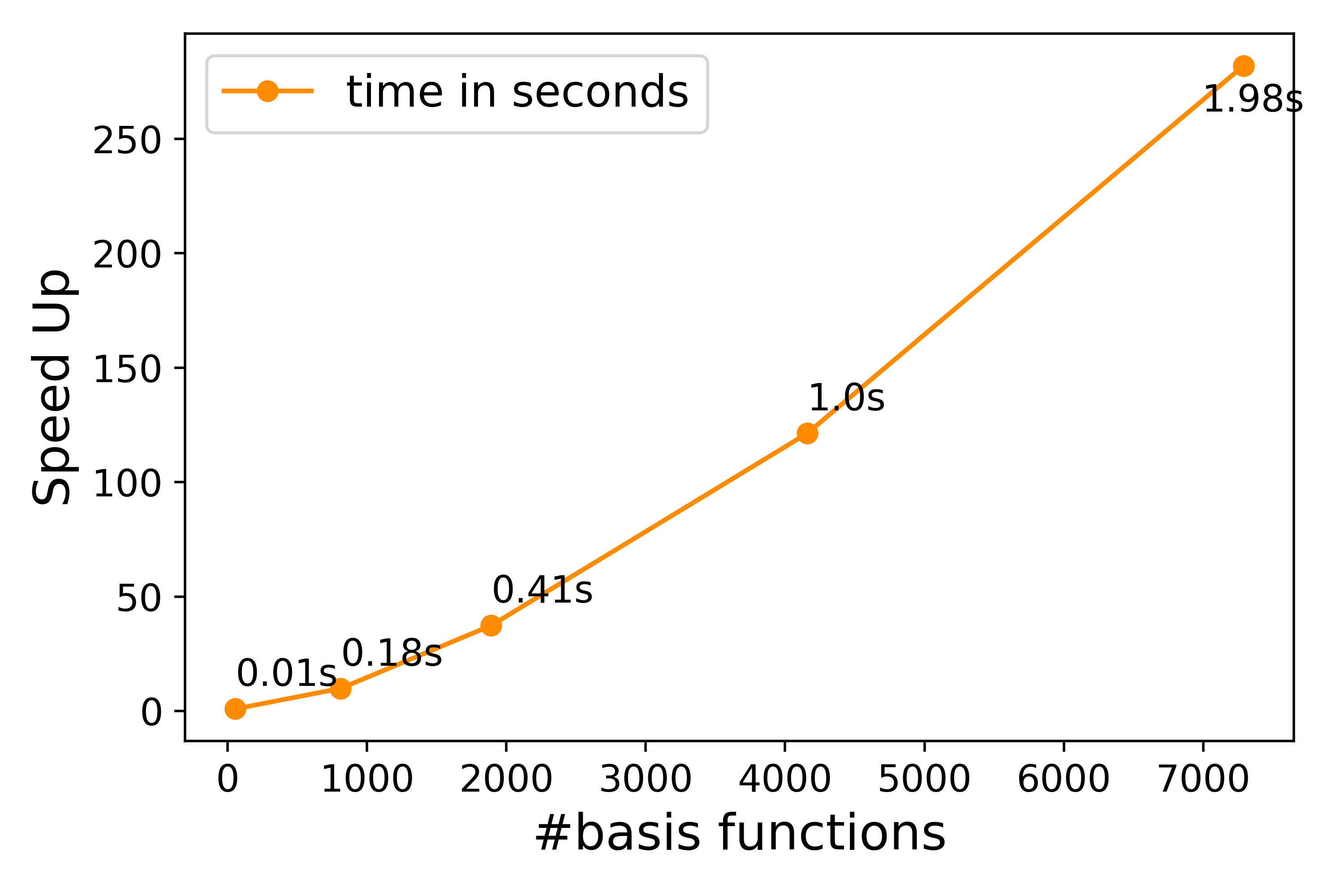
The computational efficiency of our approach is summarized in Fig. 5 where we report the SC/PL Speed Up in generating the self-energies terms for several SC sizes. The result shows that the CPU time could be accelerated by a factor 280 for the largest SC, reducing the time from to sec.
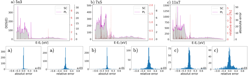
To verify that increasing the SC size does not deteriorate the accuracy, we evaluate the density of states (DOS) for a selection of SC sizes. The DOS is given by the formula:
| (7) |
From Eq. (7) we can see that this quantity includes both diagonal and off diagonal errors into one number. The energy-resolved DOS is shown in the top panel of Fig. 6(a-c) for varying . In all considered cases, the DOS obtained by a single PL agrees almost perfectly with the SC reference, thus confirming the strength and validity of our scheme. The absolute and relative errors (with the error-axis on the right side of top panel in Fig. 6(a-c)) are overlaid on the DOS curves. Both errors are more pronounced at the position of the peaks in the DOS curves. From the distribution of the error summarized in the histograms in the bottom panel of Figs. 6(a-c) we observe that the variance increases with the SC size. However, the maximum error does not show a SC-size dependence as can be seen in Table I.
| Maximum error | ||
|---|---|---|
| absolute error | relative error | |
| 5x3 | 31.13 | 0.092 |
| 7x5 | 9.22 | 0.019 |
| 11x7 | 42.21 | 0.04 |
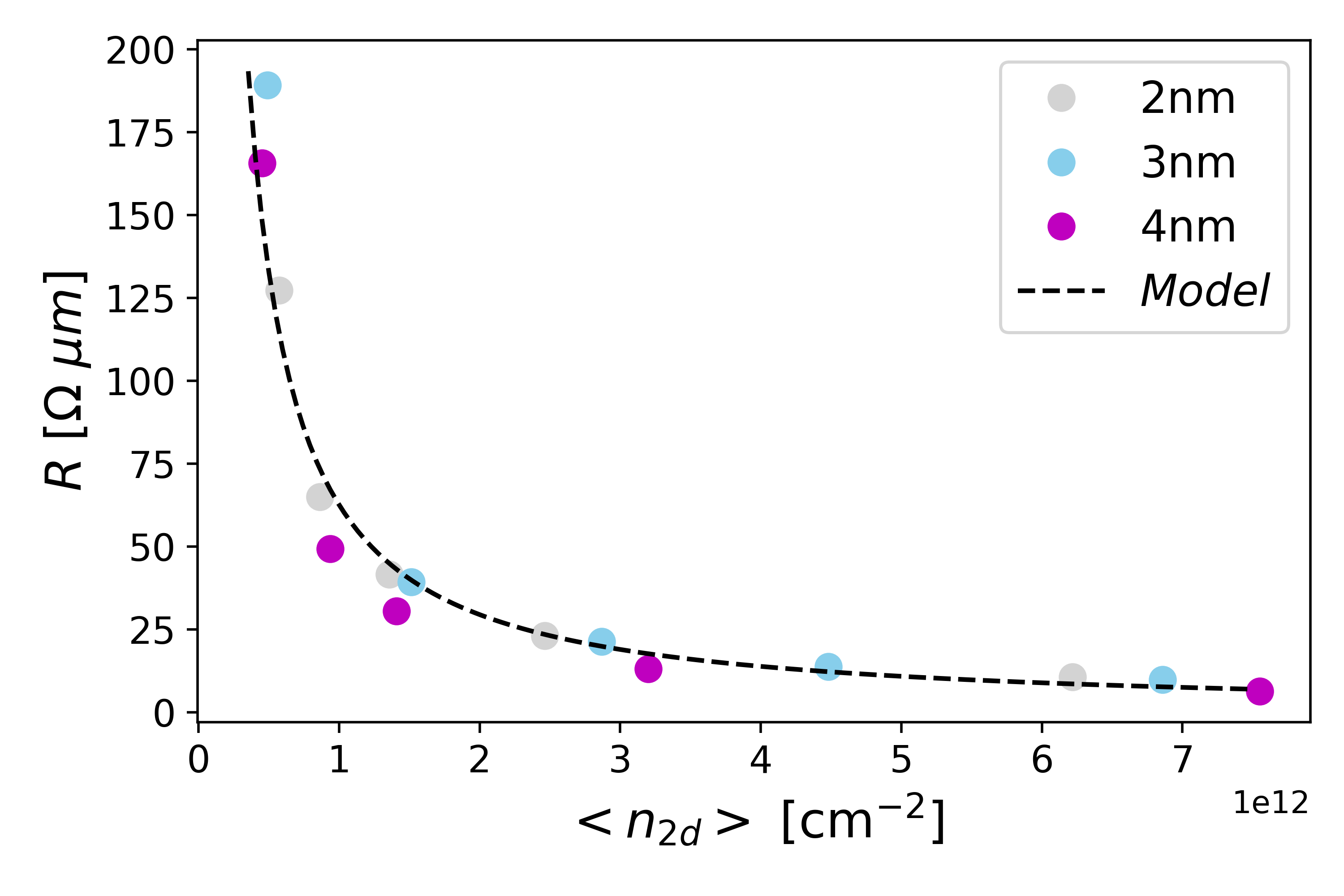
As an application of the proposed method, we investigate the electrical resistance between SiNWs and metal contacts as a function of the carrier density for various diameters. We consider three SiNWs models with and nm diameters. Fig. 7 shows that i) exhibits a clear dependence (with ) and ii) it is weakly affected by the diameter. This confirms that is dominated by the quasi-Fermi level drop near the contact regions [7].
IV CONCLUSIONS
We developed an algorithm to efficiently compute the self-energy matrices of large quasi-1D channels without sacrificing accuracy. By partitioning the contacts into PLs, we are able to significantly reduce the simulation time and to evaluate the electrical resistance of SiNWs with metallic contacts. This algorithm is key to simulate more realistic nanostructures with bulk-like contacts.
References
- [1] L. Bourdet, J. Li, J. Pelloux-Prayer, F. Triozon, M. Cassé, S. Barraud, S. Martinie, D. Rideau, and Y.-M. Niquet, “Contact resistances in trigate and finfet devices in a non-equilibrium green’s functions approach,” Journal of Applied Physics, vol. 119, no. 8, p. 084503, 2016.
- [2] M. L. Sancho, J. L. Sancho, and J. Rubio, “Quick iterative scheme for the calculation of transfer matrices: application to mo (100),” Journal of Physics F: Metal Physics, vol. 14, no. 5, p. 1205, 1984.
- [3] K. S. Thygesen, “Electron transport through an interacting region: The case of a nonorthogonal basis set,” Physical Review B, vol. 73, no. 3, p. 035309, 2006.
- [4] S. E. Mohney, Y. Wang, M. A. Cabassi, K. Lew, S. Dey, J. M. Redwing, and T. Mayer, “Measuring the specific contact resistance of contacts to semiconductor nanowires,” Solid-state electronics, vol. 49, no. 2, pp. 227–232, 2005.
- [5] J. Enkovaara, C. Rostgaard, J. J. Mortensen, J. Chen, M. Dułak, L. Ferrighi, J. Gavnholt, C. Glinsvad, V. Haikola, H. Hansen, et al., “Electronic structure calculations with gpaw: a real-space implementation of the projector augmented-wave method,” Journal of physics: Condensed matter, vol. 22, no. 25, p. 253202, 2010.
- [6] A. R. Dmitry, Theory of Quantum Transport at Nanoscale: An Introduction. Springer.
- [7] D. Rideau, F. Monsieur, O. Nier, Y. Niquet, J. Lacord, V. Quenette, G. Mugny, G. Hiblot, G. Gouget, M. Quoirin, et al., “Experimental and theoretical investigation of the ‘apparent’mobility degradation in bulk and utbb-fdsoi devices: A focus on the near-spacer-region resistance,” in 2014 International Conference on Simulation of Semiconductor Processes and Devices (SISPAD), pp. 101–104, IEEE, 2014.