Modulating Effect of Evanescent Waves on Thin-Film Growth
Abstract
Atomic-scale smooth thin films are keys to successful integration and proper function of many multilayer-structured devices. However, the intrinsic island-like growth mode prevents human being from realizing such ultrasmooth films of many important functional materials. To solve this problem, we propose a negative entropy-infusing method that employs evanescent waves to enhance the downward interlayer diffusion of adatoms and thus transform the island-like growth mode to the layer-by-layer growth mode. The formulas of the optical force and the lowered diffusion barrier were derived, and the application of this theory on a simplified example demonstrates significantly improved surface morphologies through numerical simulations.
I i. Introduction
For most integrated optoelectronic devices which function on the basis of heterojunctions, the sharpness of the interfaces is a key parameter determining the quality of the devices [1]. The fabrication success rate, consistency and working life of heterojunction devices are all related to the surface roughness of the component thin films, so controlling the surface roughness of component thin film is one of the key factors for optimizing heterojunction devices. But as a complex phenomenon, surface morphology of growing thin films is determined by many physics factors (non-uniform distribution in flux density, energy and momentum of incident species, kinetic energy, momentum, growth temperature, growth rate, sticky coefficient, diffusion, Ehrlich-Schwoebel barrier (ESB) [2, 3, 4] and so on) and physics effects (the random distribution effect, the anistropic growth rate effect, surface energy effect, strain effect, shadowing effect [5], quantum size effect [6, 7], steering effect [8], etc.). Optimizing all of the showing-up factors is a quite time-consuming solution usually adopted for achieving ultra-smooth surface, but this solution may not work for many complex compound functional materials.
In fact, the applications of surface morphologies of thin films can be classified into two categories. One category is utilizing rough surfaces, which can be achieved using many methods such as surface etching, glancing-angle deposition [5], and various other surface nanostructure fabrication techniques. The other category utilizes atomic-scale smooth surfaces or interfaces, which cannot be always satisfied because not every material can grow in a layer-by-layer mode. For example, to fabricate sandwich-type Josephson junctions using two YBa2Cu3O7-δ (YBCO) layers sandwiching an insulating layer between, the middle layer must be both insulating and of a uniform thickness around the superconducting coherence length (13.51.5Å along a,b-axis) of YBCO simultaneously [9], which means at least one YBCO layer and the insulating layer must have atomic-scale smooth surfaces. However, YBCO thin film does not grow in a layer-by-layer mode, so high-temperature superconducting computers based on YBCO have been unavailable so far. Therefore, if we invent a universally usable modulating method of altering thin-film growth mode from the island-like (Volmer-Weber) growth to a 2-dimensional (layer-by-layer or step-flow) mode, we can not only open up new research fields that rely on atomic-scale smooth thin films, but also realize the industrial applications of important functional materials and thus greatly promote new technology developments, which is of epoch-making significance.
To achieve atomic-scale smooth surface of a thin film material growing intrinsically in an island-like way, its growth mode must be altered into 2D growth manner. A basic train of thought is that considering the surface roughness is a kind of disorder (surface entropy) caused in a large degree by the random surface diffusion, we need infuse negative entropy into surface to break the randomness of adatom diffusions on the growing nuclei or islands for decreasinge surface roughness. In this article, we come up with a method of using evanescent waves (EW) to enhance the downward interlayer diffusion and suppress the upward interlayer diffusion, thus smoothen the surface of a growing thin film. The article is organized as follows: First, we introduce the main idea of the modulating effect of EW on a growing thin film. Then, we derived the formulas of the optical force exerted on adatoms by EW and the lowered part of the diffusion barrier. In the following, to illustrate the feasibility of this method using an example, the diffusion barriers without EW and with EW of different amplitudes were simulated on Ag thin film, and to visualize the modulating effect on its surface morphology, Kinetic Monte Carlo simulations were performed based on the quasi-minimum energy paths (quasi-MEPs) and ESBs of Ag(100) surface obtained from DFT calculations. Finally, the ubiquitousness of this method was discussed. The significant enhancement of downward interlayer diffusion by EW theoretically verify the feasibility of this method, and experimental tests are suggested using time-resolved x-ray scattering (trXRS) [10] and grazing-incidence x-ray photon correlation spectroscopy (GIXPCS) [11].
II ii. Principles
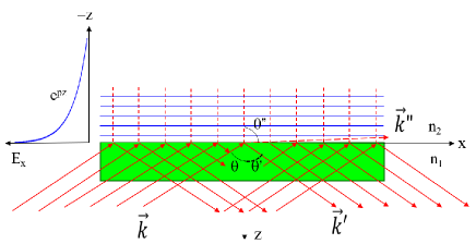
It is well known that total reflection produces evanescent wave field in the optically thinner medium [12]. As depicted in Fig.1, when a laser beam is incident onto a thin film from the substrate side with an incident angle larger than the critical angle , total reflection happens at the thin film-vacuum interface and an EW field is generated at the vacuum side near the thin film surface. The electric field of EW parallel to the reflection plane is a strong gradient field which can polarize atoms and exert a net attraction force pulling the polarized atoms downwards to the interface. Therefore we can use this attraction force to enhance the downward diffusion and suppress the upward diffusion of the adatoms on the nuclei or islands of a growing thin film, which should result in a smoothened surface.
According to fundamental optics principles, the electric field of EW can be derived
| (1) |
where is angular frequency, is the wave vector of incident wave, denotes the incident angle, and , represent the dielectric constants of Medium 1 and 2, respectively. The direction of the electric field depends on its polarization state.
Based on Lorentz effective field theory [13, 14, 15], the local electric field at position occupied by an atom can be obtained by summation of the external electric field at this site and the fields induced by dipole oscillators around the atom, which can be expressed as [13, 16]
| (2) |
| (3) |
where is the external electric field at position , denotes the dipole moment at position , and represents the electric field at induced by the dipole oscillator at . Here, the retardation effect is ignored due to the small separation between two adatoms, i.e. quasi-static approximation.
Let be the polarizability of adatom at , the dipole moment at that position can be obtained
| (4) |
| (5) |
where and is given by the Clausius-Mossotti relation:
| (6) |
where represents the size of adatoms.
To obtain the self-consistent solutions of of dielectric grains with arbitrary shape, an iterative method can be employed. Then, using Maxwell tensor method we can obtain the optical force on atom at position [12]
| (7) |
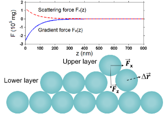
As illustrated in the bottom part of Fig.2 where Ag adatoms on is used as an example, the optical force include two components, one is gradient force (GF). Its direction points to the interface, pulling adatoms to move downwards, favorable to downward interlayer diffusion. Because the light experiences scattering by the adatoms and energy loss during propagation, EW also generates a scattering force (SF) along its propagating direction.[17]. The upper part of Fig.2 shows the z-dependence of GF and SF, calculated using real data of Ag adatoms on substrate [18,19] with a 50 watt 440 nm blue laser focused down to a 10 micron spot size. Calculations shows that the optical forces are much larger than the gravities and similar z-dependence curves also exists for other kinds of metal adatoms, as shown in Fig.1S in the Supplemental Material.
The surface morphology of a growing thin film is determined by many atomic processes mainly including deposition, intralayer diffusion, interlayer diffusion, nucleation and re-evaporation. Among them interlayer diffusion plays the most important roles in shaping surface morphology, which processes in two ways. One is that the diffusing atoms hop over the step to the neighboring layers, which is called hopping mechanism; the other is that the atoms on the step squeeze into the lower layer, and the nearest neighbor atoms in the lower layer diffuse, which is called exchange mechanism. Because a hopping adatom must experience a configuration of lower coordination number (CN) that corresponds to a higher diffusion barrier, the exchange process usually is more favorable than the hopping process, which is supported by many researches.[20, 21, 22] Therefore, at least for the growth of metal thin films the exchange mechanism is the dominant process in interlayer diffusions. Consequently, this process can represent real interlayer diffusions for verifying the effectiveness of the modulating effect of EW on thin-film growth.
We first discuss the adatom diffusion under no EW. In a diffusion process, an adatom diffuses to the nearest-neighboring position with diffusion rate . According to Boltzmann statistics and Arrhenius formula, the diffusion rate can be expressed as
| (8) |
where is Boltzmann constant, is the vibrational frequency, is the temperature, and is the diffusion energy barrier.
With EW field applied, the gradient force of EW pulls the adatoms on the step edges to squeeze into the lower layer more readily while in upward diffusion the adatoms need to overcome the GF by doing extra work, therefore the downward diffusions get promoted and the upward diffusions are suppressed. Because the light frequency is much higher than the vibrational frequency of adatoms that is about to [1, 23], the optical force during a diffusion move can be averaged into an invariable local optical force field (LOFF) . With setting the position of zero potential energy at the initial site of the diffusing adatoms, we can calculate the diffusion barriers via - simulations, and in the case with EW, the LOFF potential energy should be appended to .
| (9) |
where represents the atomic position, and can be obtained from our theoretical model with atomic diffusion path
| (10) |
Therefore, the diffusion rate can be rewritten as
| (11) |
where is the peak of the energy curve (the energy of initial state was set as zero), that is, the new diffusion barrier with EW field applied. Eq.(9) and Eq.(10) are valid in calculating both the ESBs and the normal intralayer-diffusion barriers.
III iii. Numerical experiments
To demonstrate the modulating effect of EW on adatoms diffusions using an example, the diffusion barriers without EW and with EW of different amplitudes were simulated on the growth of Ag thin film. To further simplify the simulations meanwhile without losing generality, we use the dominant exchange process as the representative of real interlayer diffusions to examine the enhancing effect of EW on interlayer diffusions. Therefore no other processes such as hopping across steps, edge diffusion or detachment from island edges were included in the simulations (according to the physics picture of EW-adatom interaction, the field of EW also enhance the net downward crossing-edge diffusion as explained in the following section). Our numerical experiments combine the above theoretical formulas and the DFT simulations that are performed using plane wave-based Vienna simulation package (VASP) [24] for the purpose of finding MEPs of diffusions. We adopted the Perdew-Burke-Ernzerhof form of the generalized gradient approximation for exchange-correlation functional [25]. Kohn-Sham wave functions are described by a plane wave basis est with cut-off energy of 400 eV. The thickness of vacuum layer is set up to 17 angstrom to eliminate the influence from the periodic pattern in the direction perpendicular to the surface. The diffusion paths and barriers for adatoms are evaluated using Nudge Elastic Band (NEB) method [26, 27].
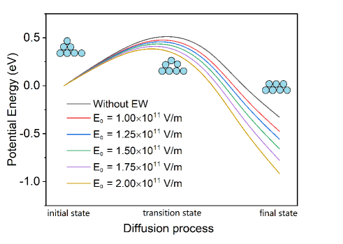
We selected a 33 supercell of Ag(100) films with a K-mesh of 331. The initial sites of adatoms were set on the upper monolayer (ML), and the process of their interlayer diffusions from the upper ML to the adjacent lower ML were simulated. According to the diffusion path from the DFT calculations, the potential energy landscape modified by the EW effect was obtained from and , as depicted in Fig.3. It is obvious that EW field lowers the downward interlayer diffusion barrier of adatoms, which is favorable to downward interlayer diffusion in the dominant exchange process, and the larger the incident light wave amplitude in Eq(1) becomes, the lower the barrier is.
The calculated diffusion barrier without EW is 0.54 eV, which is consistent with the previous studies (0.52 eV) [21]. With EW applied, the ESB decreases significantly, for example, an incident beam of V/m can lower the ESB of the interlayer diffusion along the direction of SF by , as Fig.3 shows. More details of the variations of barriers can be found in Table.1S of Supplemental Material. More significantly, the energy of final state is lowered more compared with no EW situation, which means the possibility of diffusing from lower layers to upper layers tend to zero, which further enhances the 2-dimensional growth behaviors. Although the GF also shrinks the interlayer spacing and alters the MEPs by reshaping the surface potential landscape, fortunately the GF is too small to change the MEPs noticeably, which makes it reasonable to take the calculated MEPs under no EW as the quasi-MEPs under EW in the calculations based on Eq.(9) and Eq.(10).
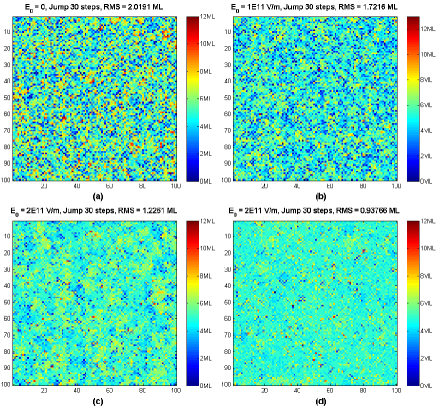
To visualize the modulating effect of EW, we carried out Kinetic Monte Carlo simulations of Ag(100) thin-film growth based on the results of quasi-MEPs. Fig.4 illustrates the simulation results using the simplified model to grasp the main physics, in which 50000 deposited adatoms land on an area of 100100 lattice points, then are forced to diffuse with 30 jumping steps; when adatoms diffusing across the boundaries, periodic diffusion condition is used, i.e., the adatoms diffusing out of the simulated deposition area from one side enter the area from the other side. The striking comparison between the roughnesses of films with and without EW demonstrates its effectiveness. The details of the simulations can be found in Supplemental Material. It is noteworthy that the unidirectional nature of SF lead to the asymmetry of diffusion and thus affects smoothness of thin film. Compared with the effect of both the GF and the SF of EW, mere GF works better for smoothing surfaces, as shown in Fig 4.(d). The SF can be cancelled using two symmetrically incident beams in practical experiments.
IV iv. Discussion
Because EW field can polarize any adatom and thus exert gradient force to enhance the downward interlayer diffusion, from this principle it can be concluded that this approach works universally for any material. This conclusion is very logic and solid although it has not been verified by comprehensive simulations or real experiments on the growth of complex compound thin films. It can be imagined that at any delicate near-balance state between downward and upward interlayer diffusions, even a small force can break their original quasi-balance. This should hold not only for exchange process but also for hopping process across steps, because, although the GF increases the ESB a little for adatoms hopping downward, it lowers the energy of the system with adatoms at the lower layers more since the upward displacement of an adatom in a downward crossing-step hopping process is much smaller than its downward displacement (as shown in Fig.2), and thus upward diffusing adatoms at lower layers have to overcome a larger barrier with EW applied. As a result, the EW-caused reduction in downward hopping rate can be over-compensated by the increased suppression of upward diffusion by EW. Therefore, the net downward interlayer diffusion is increased by EW in hopping process as well. Besides, in our model simulations, only 30 jumping diffusion steps have already produced obvious improvements of surface morphologies. In real cases, the trial jumping frequency around 1 Hz can generate much more jumping steps even within 0.1 second, which would make the actual smoothening effect of EW much better than that in our model calculations.
V v. Conclusion
In conclusion, the theory of the modulating effect of evanescent waves on thin-film growth is created with the formulas of the optical force and the lowered diffusion barrier of adatoms in the EW field being derived. Application of the theory on a thin film-on-substrate model using silver growth as an example demonstrates the increased net downward interlayer diffusion rate of adatoms. The simulations illustrate that EW can smoothen the surface of a growing thin film. To the best of our knowledge, this modulation method for enhancing surface flatness has not been tried hitherto. Experiments combining trXRS with GIXPCS are suggested to test this modulating effect.
Acknowledgements.
This research is supported by Chinese Academy of Sciences under agreement CAS No. 11U153210485 and by NSFC of China under Contract No. Y611U21. TCC is supported by the U.S. Department of Energy (DOE), Office of Science, Office of Basic Energy Sciences, Division of Materials Science and Engineering, under Grant No. DE-FG02-07ER46383.References
- [1] Electronic Thin Film Sciences: For Electrical Engineering and Materials Scientists, K.-N. Tu, J. W. Mayer, L. C. Feldman, Macmillan College Publishing Company, Inc., 1992.
- [2] R.L. Schwoebel, E.J. Shipsey, Step Motion on Crystal Surfaces, J. Appl. Phys. 37, 3682 (1966)
- [3] R.L. Schwoebel, Step Motion on Crystal Surfaces II, J. Appl. Phys. 40, 614 (1969)
- [4] G. Ehrlich, F.G. Hudda, Atomic View of Surface Self-Diffusion: Tungsten on Tungsten, J. Chem. Phys. 44, 1039 (1966)
- [5] Paritosh, D. J. Srolovitz, Shadowing effects on the microstructure of obliquely deposited films, J. App. Phys. 91,1963 (2002).
- [6] H. Hong, C.-M. Wei, M.Y. Chou, Z. Wu, L. Basile, H. Chen, M. Holt, T.-C. Chiang, Alternating Layer and Island Growth of Pb on Si by Spontaneous Quantum Phase Separation, Phys. Rev. Lett. 90, 076104 (2003).
- [7] M.M. Özer, C.-Z. Wang, Z. Zhang, H. H.Weitering, Quantum Size Effects in the Growth, Coarsening, and Properties of Ultra-thin Metal Films and Related Nanostructures, J. Low Temp. Phys. 157, 221 (2009).
- [8] S. van Dijken, L.C. Jorritsma, B. Poelsema, Steering-Enhanced Roughening during Metal Deposition at Grazing Incidence, Phys. Rev. Lett. 82, 4038 (1999).
- [9] D. Fuchs, E. Brecht, P. Schweiss, I. Loa, C. Thomsen, R. Schneider, Growth and characterization of a-axis oriented YBa2Cu3O7-x thin films on (100) LaSrGaO4 substrates, Physica C 280, 167 (1997).
- [10] H.-H. Wang, In-situ monitoring of EuTiO3 and SrTiO3 film growth using time-resolved X-ray scattering during pulsed-laser deposition, Chin. Phys. C 33, 1 (2009).
- [11] R.L. Headrick, J.G. Ulbrandt, P. Myint, J. Wan, Y. Li, A. Fluerasu, Y. Zhang, L. Wiegart, K.F. Ludwig Jr, Coherent X-ray measurement of step-flow propagation during growth on polycrystalline thin film surfaces, Nat. Comm. 10, 2638 (2019).
- [12] Principles of Optics, M. Born, E. Wolf, The Macmillan Company, 1959.
- [13] Electromagnetics and Calculation of Fields, Nathan Ida, Joao P.A. Bastos, New York, Springer, 1997.
- [14] H.A. Lorentz, Theory of Electrons, 2nd Ed Tuebner, Leipzig, 1916.
- [15] C. Kittel, Introduction to Solid State Physics, 5th ed. Wiley, New York, 1976.
- [16] J.D. Jackson, Classical Electrondynamics, Wiley, New York, 1962
- [17] M. Nieto-Vesperinas, P. C. Chaumet, A. Rahmani, Near-field photonic forces, Phil. Trans. R. Soc. Lond. A 362, 719–737 (2004).
- [18] M.A. Ordal, L.L. Long, R.J. Bell, S.E. Bell, R.R. Bell, R.W. alexander, J., C.A. Ward, Optical properties of the metals Al, Co, Cu, Au, Fe, Pb, Ni, Pd, Pt, Ag, Ti, and W in the infrared and far infrared, Applied Optics 22, 1099-1120 (1983).
- [19] M.J. Dodge. Refractive Index, in M.J. Weber (ed.), Handbook of Laser Science and Technology, Vol. IV, Optical Material: Part 2, CRC Press, Boca Raton, 1986
- [20] R. Stumpf, M. Scheffler, Theory of Self-Diffusion at and Growth of Al(111), Phys. Rev. Lett. 72, 254 (1994)
- [21] B.D. Yu, M. Scheffler, Anisotropy of Growth of the Close-Packed Surfaces of Silver, Phys. Rev.Lett. 77, 1095 (1996)
- [22] P.J. Feibelman, Interlayer Self-Diffusion on Stepped Pt(111), Phys. Rev. Lett. 81, 168 (1998)
- [23] K. Sarakinos, A review on morphological evolution of thin metal films on weakly interacting substrates, Thin Solid Films 688, 137312 (2019).
- [24] G. Kresse, J. Hafner, Ab initio molecular dynamics for liquid metals, Phys. Rev. B 47, 558 (1993)
- [25] J.P. Perdew, K. Burke, and M. Ernzerhof, Generalized Gradient Approximation Made Simple, Phys. Rev. Lett. 77, 3865 (1996).
- [26] G. Henkelman, B.P.Uberuaga, H. Jonsson, A climbing image nudged elastic band method for finding saddle points and minimum energy paths, J. Chem. Phys. 113, 9901 (2000)
- [27] G. Henkelman, H.Jonsson, Improved tangent estimate in the nudged elastic band method for finding minimum energy paths and saddle points, J. Chem. Phys. 113, 9978 (2000)