Fundamental Limits on Energy-Delay-Accuracy of In-memory Architectures in Inference Applications
Abstract
This paper obtains fundamental limits on the computational precision of in-memory computing architectures (IMCs). An IMC noise model and associated SNR metrics are defined and their interrelationships analyzed to show that the accuracy of IMCs is fundamentally limited by the compute SNR () of its analog core, and that activation, weight and output precision needs to be assigned appropriately for the final output SNR . The minimum precision criterion (MPC) is proposed to minimize the ADC precision. Three in-memory compute models - charge summing (QS), current summing (IS) and charge redistribution (QR) - are shown to underlie most known IMCs. Noise, energy and delay expressions for the compute models are developed and employed to derive expressions for the SNR, ADC precision, energy, and latency of IMCs. The compute SNR expressions are validated via Monte Carlo simulations in a CMOS process. For a 512 row SRAM array, it is shown that: 1) IMCs have an upper bound on their maximum achievable due to constraints on energy, area and voltage swing, and this upper bound reduces with technology scaling for QS-based architectures; 2) MPC enables to be realized with minimal ADC precision; 3) QS-based (QR-based) architectures are preferred for low (high) compute SNR scenarios.
I Introduction
In-memory computing (IMC) [1, 2, 3, 4] has emerged as an attractive alternative to conventional von Neumann (digital) architectures for addressing the energy and latency cost of memory accesses in data-centric machine learning workloads. IMCs embed analog mixed-signal computations in close proximity to the bit-cell array (BCA) in order to execute machine learning computations such as matrix-vector multiply (MVM) and dot products (DPs) as an intrinsic part of the read cycle and thereby avoid the need to access raw data.
IMCs exhibit a fundamental trade-off between its energy-delay product (EDP) and the accuracy or signal-to-noise ratio (SNR) of its analog computations. This trade-off arises due to constraints on the maximum bit-line (BL) voltage discharge and due to process variations, specifically spatial variations in the threshold voltage , which limit the dynamic range and the SNR. Additionally, IMCs also exhibit noise due to the quantization of its input activation and weight parameters and due to the column analog-to-digital converters (ADCs). Henceforth, we use “compute SNR” to refer to the computational precision/accuracy of an IMC, and “precision” to the number of bits assigned to various signals.
Today, a large number of IMC prototype ICs and designs have been demonstrated [5, 6, 7, 8, 9, 10, 11, 12, 13, 14, 15, 16, 17, 18, 19, 20, 21, 22, 23, 24, 25, 26, 27]. While these IMCs have shown impressive reductions in the EDP over a von Neumann equivalent with minimal loss in inference accuracy, it is not clear that these gains are sustainable for larger problem sizes across data sets and inference tasks. Unlike digital architectures whose compute SNR can be made arbitrarily high by assigning sufficiently high precision to various signals, IMCs need to contend with both quantization noise as well as analog non-idealities. Therefore, IMCs will have intrinsic limits on their compute SNR. Since the compute SNR trades-off with energy and delay, it raises the following question: What are the fundamental limits on the achievable computational precision of IMCs?
Answering this question is made challenging due to the rich design space occupied by IMCs encompassing a huge diversity of available memory devices, bitcell circuit topologies, circuit and architectural design methods. Today’s IMCs tend to employ ad-hoc approaches to assign input and ADC precisions or tend to overprovision its analog SNR in order to emulate the determinism of digital computations.
Recently in [28], we have attempted to answer the above question for the specific IMC in [6]. A comprehensive analytical understanding of the relationship between precision, compute SNR, energy, and delay across all types of IMCs, is presently missing. This paper fills this gap (preliminary results in [29]) by: 1) defining compute SNR metrics for IMCs, 2) developing a systematic methodology to obtain a minimum precision assignment for activations, weights and outputs of fixed-point DPs realized on IMCs to meet network accuracy requirements, and 3) employing this methodology to obtain the limits on achievable compute SNR of commonly employed IMC topologies, and quantify their energy vs. accuracy trade-offs.
This paper is organized as follows: Section II presents preliminaries related to signal and DP quantization. Section III proposes the IMC noise model and associated compute SNR metrics. Section IV presents analytical expressions for the compute SNR of three different IMCs. Simulation results quantifying various trade-offs including those between energy and accuracy are presented in Section V. Section VI summarizes the key takeaways for designing IMCs.
II Notation and Preliminaries
II-A General Notation
We employ the term signal-to-quantization noise ratio (SQNR) when only quantization noise (denoted as ) is involved. The term SNR is employed when analog noise sources are included and use to denote such sources. SNR is also employed when both quantization and analog noise sources are present.
II-B The Additive Quantization Noise Model
Under the additive quantization noise model, a floating-point (FL) signal quantized to bits is represented as , where is the quantization noise assumed to be independent of the signal .
If and where is the quantization step size and denotes the uniform distribution over the interval , then the signal-to-quantization noise ratio () is given by:
| (1) |
where , , and is the peak-to-average (power) ratio (PAR) of . Equation (1) quantifies the familiar SQNR gain per bit of precision.
II-C The Dot-Product (DP) Computation
Consider the FL dot product (DP) computation defined as:
| (2) |
where is the DP of two -dimensional real-valued vectors (weight vector) and (activation vector).
In DNNs, the dot product in (2) is computed with (signed weights), input (unsigned activations assuming the use of ReLU activation functions) and output (signed outputs). Assuming the additive quantization noise model from Section II-B, the fixed-point (FX) computation of the DP (2) with precisions (weight), (activation), and (output), is described by:
| (3) | ||||
| (4) |
where and are the quantized weight and activation vectors, respectively, is the total input (weight and activation) quantization noise seen at the output (output referred quantization noise), and is the additional output quantization noise due to round-off/truncation in digital architectures or from the finite resolution of the column ADCs in IMC architectures.
Assuming that the weights (signed) and inputs (unsigned) are i.i.d. random variables (RVs), the variances of signals in (4) are given by:
| (5) |
where is the variance of the weights, , and are the weight, activation, and output quantization step-sizes, respectively.
III Compute SNR Limits of IMCs
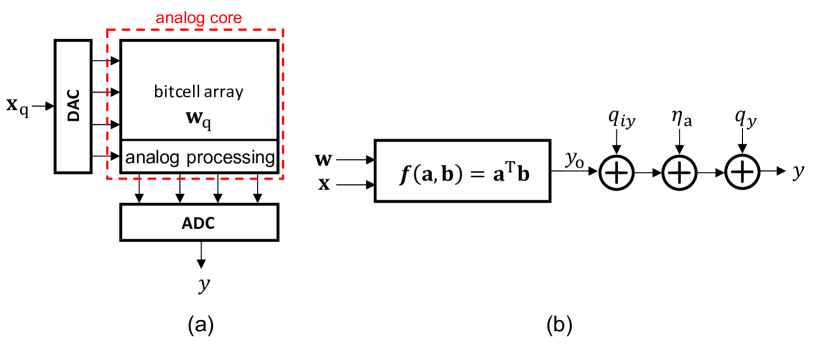
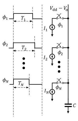
We propose the system noise model in Fig. 1 for obtaining precision limits on IMCs. Such architectures (Fig. 1(a)) accept a quantized input () and a quantized weight vector () to implement multiple FX DP computations of (4) in parallel in its analog core. Hence, unlike digital architectures, IMC architectures suffer from both quantization and analog noise sources such as SRAM cell current variations, thermal noise, and charge injection, as well as the limited headroom, which limits its compute SNR.
III-A Compute SNR Metrics for IMCs
The following equations describe the IMC noise model in Fig. 1:
| (6) |
where is the ideal DP value defined in (2), is the output referred quantization noise, is the analog noise term comprising both clipping noise due to limited headroom and other noise sources , and is the output quantization noise introduced by the ADC.
We define the following fundamental compute SNR metrics:
| (7) |
where is the analog SNR, is the output referred SQNR due to input (weight and activation) quantization and is given by:
| (8) |
where and are the PARs of the (unsigned) activations and (signed) weights, respectively, and is the digitization SQNR solely due to ADC quantization noise and is given by:
| (9) |
obtained by the substitutions: and in (1).
From (6) and (7), it is straightforward to show:
| (10) | ||||
| (11) |
where is the pre-ADC SNR and is the total output SNR including all noise sources. Note: (10)-(11) can be repurposed for digital architectures by setting since quantization is the only noise source thereby implying . Equations (8)-(9) indicate that and can be made arbitrarily large by assigning sufficiently high precision to the DP inputs ( and ) and the output (). Thus, from (10)-(11), in IMCs is fundamentally limited by which depends on the analog noise sources as one expects.
III-B Maximizing in IMCs
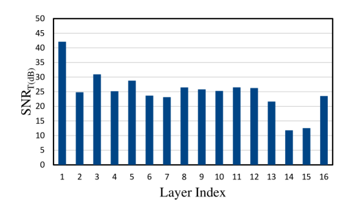
Prior work based on post-training quantization [30, 31], indicates the requirement - (see Fig. 2) for the inference accuracy of an FX network to be within 1% of the corresponding FL network for popular DNNs (AlexNet, VGG-9, VGG-16, ResNet-18) deployed on the ImageNet and CIFAR-10 datasets. While in-training quantization methods [32] can reduce these requirements, a precision of 4-b () is generally found to be [33] sufficient. To meet this requirement, digital architectures choose and such that , and then choose sufficiently high to guarantee so that .
In contrast, for IMCs, we first need to ensure that so that can be made to approach with appropriate precision assignment. Such a precision assignment can be easily derived from (10)-(11) as shown below:
- 1.
-
2.
Assign sufficiently a high value for such that so that per (11).
For example, if then , i.e., lies within of . In this manner, by appropriate choices for , , and , IMCs can be designed such that , which, as mentioned earlier, is the fundamental limit on .
From the above discussion it is clear that the input precisions and are dictated by network accuracy requirements, while the output precision needs to be set sufficiently high for the output quantization from becoming a significant noise contributor. To ensure that a sufficiently high value for , digital architectures employ the bit growth criterion (BGC) described next.
III-C Bit Growth Criterion (BGC)
The BGC is commonly employed to assign the output precision in digital architectures [34, 30]. BGC sets as:
| (12) |
Substituting from (12) into (9) and employing the relationship , the resulting SQNR due to output quantization using the BGC is given by:
| (13) |
Recall that in order to ensure is close to its upper bound. Comparing (9) and (13), we see that, for high values of DP dimensionality , BGC is overly conservative since it assigns large values to per (12). Some digital architectures truncate the LSBs to control bit growth. The SQNR of such truncated BGC (tBGC) can be obtained directly from (9) by setting the value of .
BGC’s high precision requirements is accommodated in digital architectures by increasing the precision of arithmetic units with a commensurate increase in the computational energy, latency, and activation storage costs. However, IMCs cannot afford to use this criterion since is the precision of the BL ADCs which impacts its energy, latency, and area. Indeed, recent works [35] have claimed that BL ADCs dominate the energy and latency costs of IMCs. Such works employ the highly conservative BGC or tBGC to assign .
In the next section, we propose an alternative to BGC and tBGC referred to the minimum precision criterion (MPC), that can be employed by both digital and IMC architectures to achieve a desired with much smaller values of .
III-D The Minimum Precision Criterion (MPC)
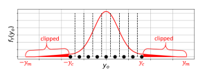


We propose MPC to reduce without incurring any loss in compared to BGC. Unlike BGC, MPC accounts for the statistics of to permit controlled amounts of clipping to occur. In MPC (see Fig. 3(a)), the output is clipped to lie in the range instead of as in BGC (see Fig. 3(b)), where is the clipping level, and bits are employed to quantize this reduced range. The clipping probability is kept to a small user-defined value, e.g., ensures that if . The resulting is given by:
| (14) |
where , and is the conditional clipping noise variance. Setting yields indicating that is a decreasing function of . Thus, (14) has the same form as (1) with an additional (last term) clipping noise factor.
MPC exploits a key insight (see Fig. 3(c)), which follows from the Central Limit Theorem (CLT) – in a -dimensional DP computation (2), grows sub-linearly (as ) as compared to the maximum which grows linearly with . Furthermore, (14) shows a quantization vs. clipping noise trade-off controlled by the clipping level . We show empirically in Section III-E that in (14) is maximized when clipping level if . This trade-off (see Fig. 3(b)) is absent in BGC and tBGC, and is critical to MPC’s ability to realize desired values of with smaller values of .
Thus, we state the following MPC-based rule for maximizing the SQNR of column ADCs in IMCs:
MPC-based SQNR Maximizing Rule
For a Gaussian signal, setting the clipping level to four times the standard deviation will maximize the SQNR for a given precision .
Some IMC designs [36] do in fact allow for clipping in the column ADCs but these levels are set empirically. The MPC-based Rule in contrast quantitatively specifies the smallest ADC precision and the optimal clipping level needed to ensure that . A lower bound on can be obtained by assuming , and substituting , and into (14), to obtain:
| (15) |
in order for . For instance, the choice yields which corresponds to as discussed in Section III-B.
III-E Simulation Results

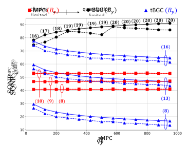
To illustrate the difference between MPC, BGC and tBGC, we assume that , so that provided per (10)-(11). We further assume DPs of varying dimension with 7-b quantized unsigned inputs and signed weights randomly sampled from uniform distributions. Substituting , , and into (8), we obtain . Thus, all that remains is to assign such that , for which there are three choices - MPC, BGC and tBGC.
Figure 4(a) compares the achieved by the three methods. Per (15), MPC meets the requirement by setting and independent of . In contrast, per (12), BGC assigns as a monotonically increasing function of to achieve the same as MPC. Furthermore, tBGC meets the requirement with but fails to do so with . Figure 4(b) shows that is maximized when , i.e., when clipping level thereby illustrating MPC’s quantization vs. clipping noise trade-off described by (14).
Figure 4 also validates the analytical expressions (8), (9), (13), and (14) (bold) by indicating a close match to ensemble-averaged values of obtained from Monte Carlo simulations (dotted).
Note: it is well-established that the theoretically optimal quantizer given an arbitrary signal distribution is obtained from the Lloyd-Max (LM) algorithm [37]. Unfortunately, the LM quantization levels are non-uniformly spaced which makes it hard to design efficient arithmetic units to process such signals. Furthermore, for as in Figure 4(b), LM achieves an which is only better than MPC. Thus, MPC offers a practical alternative to LM for assigning minimal precision to the column ADC in IMCs and the accumulator precision in digital architectures.
IV Analytical Models for Compute SNR
| In-memory Compute Model | Analog Core Precision | ADC Precision | ||||
| QS | IS | QR | ||||
| Kang et al. [6] | 8 | 8 | 8 | |||
| Biswas et al. [8] | 8 | 1 | 7 | |||
| Zhang et al. [5] | 5 | 1 | 1 | |||
| Valavi et al. [12] | 1 | 1 | 1 | |||
| Khwa et al. [11] | 1 | 1 | 1 | |||
| Jiang et al. [7] | 1 | 1 | 3.46 | |||
| Si et al. [38] | 2 | 5 | 5 | |||
| Jia et al. [39] | 1 | 1 | 8 | |||
| Okumura et al. [40] | 1 | T | 8 | |||
| Kim et al. [13] | 1 | 1 | 1 | |||
| Guo et al. [41] | 1 | 1 | 3 | |||
| Yue et al. [42] | 2 | 5 | 5 | |||
| Su et al. [15] | 2 | 1 | 5 | |||
| Dong et al. [14] | 4 | 4 | 4 | |||
| Si et al. [16] | 2 | 2 | 5 | |||
| Jiang et al. [43] | 1 | 1 | 5 | |||
| Jaiswal et al. [17] | 4 | 4 | 4 | |||
| Ali et al. [18] | 4 | 4 | 4 | |||
| Si et al. [19] | 1 | 1 | 1 | |||
| Liu et al. [20] | A | 1 | 1 | |||
| Zhang et al. [21] | 8 | 8 | 8 | |||
| Gong et al. [22] | 2 | 3 | 8 | |||
| Agrawal et al. [23] | 1 | 1 | 5 | |||
T: Ternary; A: Analog/Continuous-valued
This section derives analytical expressions for of a typical IMC. We introduce compute models that form the fundamental building blocks of IMCs and present analytical expressions for circuit domain equivalents of and in (6) for them. These are combined with algorithm and precision-dependent noise sources and to obtain . First, we show that most IMCs can be ‘explained’ via three in-memory compute models.
IV-A In-memory Compute Models
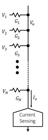
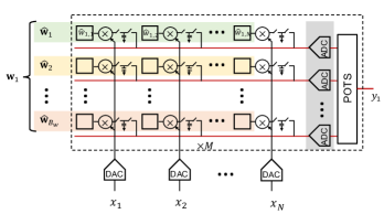
All IMCs are viewed as employing one or more in-memory compute models defined as a mapping of algorithmic variables , and in (2) to physical quantities such as time, charge, current, or voltage, in order to (usually partially) realize an analog BL computation of the multi-bit DP in (2).
Furthermore, we suggest that most IMCs today employ one or more of the following three in-memory compute models (see Fig. 5): (a) charge summing (QS) [6, 44, 9, 5]; (b) current summing (IS) [13, 7, 11, 38]; and (c) charge redistribution (QR) [12, 8, 6, 9], and conjecture that these compute models are in some sense universal in that they represent an approximation to a ‘complete set’ of practical, i.e., realizable, mappings of variables from the algorithmic to the circuit domain as shown in Table I.
Henceforth, we discuss the QS model and QR compute model and the corresponding IMC architectures referred to as QS-Arch, QR-Arch in detail since it is very commonly used. We also study compute-memory (CM) architectures [1, 6, 9] which combine the QS and QR compute models to implement a multi-bit DP.
IV-B Charge Summing (QS)
IV-B1 The QS Model
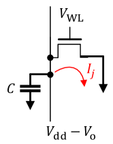
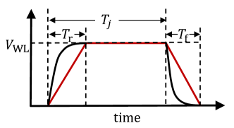
The QS model (see Fig. 5(a)) realizes the DP in (2) via the variable mapping (, , ) where the cell current is integrated over the WL pulse duration () on a BL (or cell) capacitor resulting an output voltage as shown below:
| (16) |
where is the DP output assuming infinite voltage head-room, i.e., no clipping. The cell current depends upon transistor sizes and the WL voltage , and typical values are: (a few hundred s), (tens of s), and (hundreds of ).
Noise Models: The noise contributions in QS arise from the following sources: (1) variations in the pulse-widths of current switch pulses (Fig. 5(a)); (2) their finite rise and fall times (see Fig. 6(b)); (3) spatial variations in the cell currents ; (4) thermal noise in the discharge RC-network; and (5) clipping due to limited voltage head-room. Thus, the analog DP output corresponding to is given by:
| (17) |
where is the maximum allowable output voltage, and and are the voltage domain noise due to circuit non-idealities and clipping, respectively, is the noise due to (spatial) current mismatch, and is the noise due to (temporal) pulse-width mismatch, respectively, both of which are modeled as zero mean Gaussian random variables, models the impact of finite rise and fall times of the current switching pulses, and is the integrated thermal noise voltage. Note: can be as high as 0.9 V when .
Analytical expressions to estimate the noise standard deviations , , , and , (see appendix) are provided below:
| (18) | ||||
| (19) | ||||
| (20) |
where is normalized current mismatch variance, is the delay of a -stage WL driver composed unit elements with delay each, is the standard deviation of , and are WL pulse rise and fall times (see Fig. 6(b)), is a fitting parameter in the -law transistor equation, is standard deviation of variations, is the Boltzmann constant, is the absolute temperature, and is the transconductance of the access transistor.
Note that typically the WL voltage is identical for all rows in the memory array with a few exceptions such as [5] which modulate to tune the cell current . The effects of rise/fall times and delay variations can be mitigated by carefully designing the WL pulse generators. Therefore, noise in QS is dominated by spatial threshold voltage variations. Indeed, using the typical values from Table II, we find that ranges from 8% to 25%, while ranges from 0.5% to 3%.
| Parameter | Value | Parameter | Value | |
| QS | 220 | 1.8 | ||
| 2.3 ps | 23.8 mV | |||
| - | ||||
| 0.4 V | 100 ps | |||
| QR | 0.31 fF | 0.08 fF0.5 | ||
| 0.5 | ||||
| Common Parameters | ||||
| 300 K | ||||
| 1 V | ||||
Energy and Delay Models: The average energy consumption in the QS model is given by:
| (21) |
where the spatio-temporal expectation is taken over inputs (temporal) and over columns (spatial) is the energy cost of toggling switches s. Equation (21) shows that the energy consumption in the QS model increases with array size, the supply voltage , and the mean value of the DP .
The delay of the QS model is given by where is the time required to precharge the capacitors and setup currents, and is the longest allowable pulse-width.
IV-B2 The QS Architecture (QS-Arch)
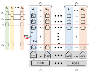
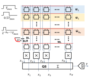
The charge summing architecture (QS-Arch) in Fig. 7(b) employs a 6T [41] or 8T [38] SRAM bitcell within the QS model (see Section IV-B). This architecture implements fully-binarized DPs on the BLs by mapping the input bit to the WL access pulse while the weights are stored across columns of the BCA so that the BC currents . The output is the voltage discharge on the BL and the capacitance is the BL capacitance in (16). QS-Arch sequentially (bit-serially) processes one multi-bit input vector in in-memory compute cycles followed by a digital summing of the binarized DPs to obtain the final multi-bit DP (2).
| QS-Arch | QR-Arch | CM | |
| Bitcell type | 6T or 8T | 8T or 10T + MOM cap | 6T |
| Analog Core Precision | Binarized () | Binary-weighted () | Multi-bit |
| Compute model used | QS | QR | QS & QR |
| Energy cost per DP | |||
| Compute model mapping | QS: QR: | ||
| 0 | |||
; is the normalized standard deviation of the bit-cell current (18); ; .
We derive the analytical expressions of architecture-level noise models for QS-Arch using those of the QS model described in Section IV-B. In QS-Arch, clipping occurs in each of the binarized DPs and contributes to the overall clipping noise variance at the multi-bit DP output. Circuit noise from each binarized DP is aggregated to obtain the final circuit noise variance . In addition, employing MPC imposed requirement on the final DP output precision (15), we obtain the lower bound on ADC precision .
Since the multi-bit DP computation in (2) is high-dimensional ( can be in hundreds), it is clear that the limited BL dynamic range e.g., in (17), will begin to dominate in (7). It is for this reason that most, if not all, IMCs resort to some form of binarization of the multi-bit DP in (2) prior to employing one of the in-memory compute models (see Table I). Ultimately, limits the number and accuracy of BL computations per read cycle and hence the overall energy efficiency of IMCs.
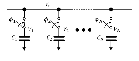
IV-C Charge Redistribution (QR)
IV-C1 The QR model
The QR model (Fig. 5(c)) is commonly employed to perform the additions in (2). The multiplications in (2) are separately computed via charging/discharging capacitor in proportion to the product () as in [12, 8], or by employing explicit multiplier circuits such as in [6, 9]. The capacitors share charge via a sequence of switching events (see Fig. 5LABEL:sub@fig:CharRe) to generate the final voltage given by:
| (22) |
The capacitors are typically metal-on-metal (MOM) capacitors with values ranging from 1 fF to 10 fF [6, 12].
Noise Models: Assuming MOM-based s, the noise contributions in QR arise from: (1) capacitor mismatch [45]; (2) charge injection due to switching [46]; and (3) thermal noise. Unlike QS, and similar to IA, the QR model does not suffer from headroom clipping noise. Hence, the DP output corresponding to in (6) is given by:
| (23) | ||||
where is the voltage domain noise term due to circuit non-idealities corresponding to in (6), is the noise is due to charge injection, is the capacitor mismatch, and is the thermal noise. Furthermore, expressions for the noise parameters in (23) can be derived as [45, 46]:
| (24) |
where is a technology- and layout-dependent Pelgrom coefficient [45], is constant that depends on the layout of the switch transistor, is the gate oxide capacitance per unit area, and and are the width and length of the switch transistor. The effect of noise in the QR compute model can be minimized by increasing the capacitors sizes at the expense of energy consumption as seen from (25) below.
Energy and Delay Models: The average energy consumption in the QR model is given by:
| (25) |
where includes energy cost for the switches s.
The delay of the QR model is given by: where is the time required for charge sharing to complete, and is the time required to precharge the capacitors to the desired voltages .
IV-C2 The QR architecture (QR-Arch)
The QR-Arch, e.g., [8], in Fig. 7(c) employs a modified BC to include a capacitor and additional switches for multiplication within the QR model. While works such as [8] employ the parasitic capacitances on the BL within the BC, an explicit MOM capacitor is assumed for simplicity. QR-Arch implements a binary weighted DP by storing the weights across rows of the BCA and by providing a multi-bit analog input to the multiplier. The multiplication is implemented by first charging the capacitor to a voltage proportional to and then discharging it based on . Multiplication is followed by a QR operation across the rows so that the final voltage across the capacitors in each row is proportional to binary-weighted DP. Thus, the QR-Arch processes one multi-bit input vector in one in-memory compute cycle to compute binary-weighted DPs that are power-of-two (POT) summed digitally to obtain the final multi-bit DP (2).
The average energy per DP (see Table III) includes (25) and which in turn includes the energy consumption of the DACs used for converting into the analog domain. The energy cost of DACs are amortized since these are shared by multiple DPs computations.
Since the QR compute model does not suffer from headroom clipping, and the lower bound on is dictated solely by MPC. The primary analog noise contributors () are the capacitor mismatch (), charge injection noise () in the switches, and thermal noise () as indicated in Table III. An alternative QR model [47, 43, 48] is to directly switch the bottom plate of the capacitors with binary outputs of the BC multiplies. Doing so leads to greater energy efficiencies and significant reduction in charge injection noise. The analysis presented in this section can be extended to such models as well.
IV-D Compute Memory
CM [1, 6, 9] in Fig. 7(c) employs a 6T SRAM BC within the QS (see Section IV-B) and QR (see Section IV-C) models. In the most general case, CM strives to implement a -b DP directly by mapping -b inputs to pulse width and/or amplitude of the WL access pulses and storing -b weights in a column-major format across cells. In practice, CM realizations such as [6] employ POT weighted WL access pulse-widths for rows so that the voltage discharge on the -th BL is proportional to the weight . The product is realized using a per-column charge redistribution-based multiplier, followed by a QR stage to aggregate the multiplier outputs. In this way, CM computes the -b DP (2) in analog in a single in-memory compute cycle.
The energy cost per DP for CM in Table III is obtained by substituting and in (21), and using (25) with . Here, is the energy consumption of the mixed-signal multiplier. The factor of 2 in first term accounts for discharge on both BL and BL-bar needed to realize signed weights [9]. The second term is the energy consumed in aggregating the column outputs using the QR model with identical capacitors .
The expression for neglects the impact of pulse width variations and other noise sources in QR since it is dominated by variations in the bit-cell current . However, the sample-accurate Monte Carlo simulations incorporte all noise sources.
The factor of in the denominator of the expression for the ADC input range due to the use of QR indicates that the loss in voltage range due to charge redistribution across capacitors.
V Simulation Results
This section describes the SNR validation methodology for validating the SNR (noise) expressions in Table III and simulation results for QS-Arch.
V-A SNR Validation Methodology
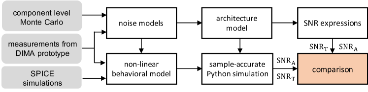
Figure 8 describes the SNR validation methodology. We obtain the QS and QR model parameters (Section IV) using Monte Carlo circuit simulations in a representative 65 nm CMOS process, with experimental validation of some of these, e.g., , from our IMC prototype ICs [49, 6] when possible.
Incorporating non-linear circuit behavior along with noise models, sample-accurate Monte Carlo Python simulations are employed to numerically calculate SNR values using ensemble averaged (over 1000 instances) statistics. We compare the SNR values obtained through sample-accurate simulations with those obtained by evaluating the analytical expressions in Table III.
The quantitative results in subsequent sections employ the QS and QR model parameter values in Table II along with QS-Arch, QR-Arch, and CM energy and noise models from Table III. An SRAM BCA with 512 rows and is assumed throughout. Energy and accuracy is traded-off of by tuning in QS-Arch and CM, and by tuning in QR-Arch We assume zero mean signed weights and unsigned inputs drawn independently from two different distributions. We set everywhere, unless otherwise stated, so that and therefore from (10). Next, we show how and trade-off with and .
V-B SNR Trade-offs in IMCs
V-B1 QS-Arch
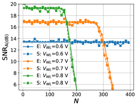
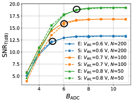
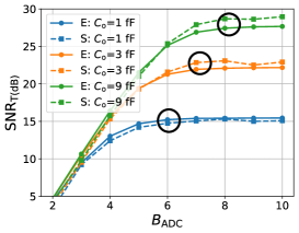
Figure 11(a) shows that the maximum achievable increases with . Further, for a fixed , QS-Arch also exhibits a sharp drop in at high values of , e.g., for and then drops with increase in . A key reason for this trade-off is that decreases while increases as is reduced (see Table III), and since limits and limits . Thus, by controlling , we can trade-off with . Specifically, increases by for every 3 dB drop in .
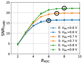
In QS-Arch, the minimum value of (see Table III) depends upon the minimum of: 1) the MPC term (15); 2) the headroom clipping term; and 3) the small case where BL discharge has a finite number of discrete levels. Figure 11(b) shows that of Fig. 11(a) when is greater than the lower bound (circled) in Table III for different values of and .
V-B2 QR-Arch
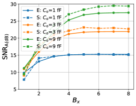
QR-Arch demonstrates a clear energy-accuracy-area trade-off as seen in Fig. 11(a). Here, improves with capacitor size but at the expense of higher energy and area costs. For instance, increasing from 1 fF to 3 fF and 9 fF leads to improvements of and , respectively.
Figure 11(b) shows that the expressions in Table III correctly predict the minimum value of ADC precision and the input range . MPC is demonstrated to greatly reduce the ADC precision requirements as for this example 6-8 bits suffice in order to maintain . In contrast, if BGC were to be employed, would have been assigned.
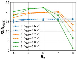
V-B3 Compute Memory
Figure 11(a) shows that the quantization noise term reduces and the headroom clipping noise increases as a function of implying an -optimal value for , e.g., peaks at and for and , respectively.
Figure 11(a) also shows another interesting trade-off, this time between headroom clipping noise and , e.g., when , is dominated by when and by when . Furthermore, both noise sources are balanced when . In fact, one can show that the clipping threshold is proportional to indicating this relationship.
V-C Impact of ADC Precision
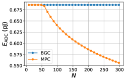
Minimizing the column ADC energy is critical to maintain IMC’s energy efficiency. ADCs in IMCs need to operate in a noise-limited regime due to the high PAR of high-dimensional DP outputs combined with severe area constraints imposed by column-pitch matching requirements. To estimate the ADC energy costs we use the following empirical model based on [48]:
| (26) |
where is the voltage range that need to be quantized, and and are empirical parameters [48] based on the recent ADCs [50, 51].
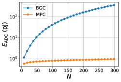
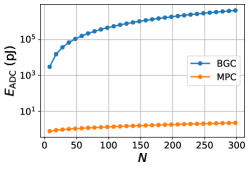
From (26), it is clear that the energy consumption of ADC decreases with and increases with . If BGC is employed, then (12) resulting in ADC energy increasing with when is constant, as in the case of QR-Arch and in CM (see Fig 12(b) and Fig 12(c)). However, in QS-Arch, therefore the ADC energy consumption in QS-Arch remains constant with (see Fig 12(a)).
On the other hand, if MPC is employed, remains constant with (Table III), and hence only depends on . In QS-Arch, reduces with as , while in QR-Arch and CM increases with as (see Fig 12(a)). Note that for QR-Arch and CM, MPC leads to significant energy savings over BGC criterion since in BGC while using MPC.
V-D Impact of Technology Scaling
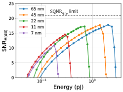
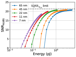
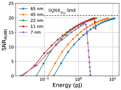
One expects IMCs to exhibit improved energy efficiency and throughput in advanced process nodes due to lower capacitance and lower supply voltage. However, the impact of technology scaling on the analog noise sources also needs to be considered. To study this trade-off, we employ the SNR and energy models from Section IV (see Table III) with parameters scaled as per the ITRS roadmap [52]. FDSOI technology is assumed for the , and nodes.
For a specific node, Fig. 13 shows that the energy cost reduces by in CM and QS-Arch, and in QR-Arch for every drop in . QS-Arch suffers a catastrophic drop in before reaching the input quantization noise limit set by (8). This drop occurs due to an increase in the clipping noise variance . In contrast, QR-Arch is able to approach quantization noise limits as it does not suffer from headroom clipping noise.
Across technology nodes, the maximum achievable in QS-Arch and CM reduces as technology scales from down to due to: 1) increased clipping probability caused by lower supply voltages, and 2) increased variations in BL discharge voltage due to smaller ratio. As a result, Fig. 13 also shows that the energy consumption, at the same , is in fact higher in 11 nm and 7 nm nodes as compared to the 22 nm node in QS-Arch and CM due to the need to employ a higher values of to control variations in implying the technology scaling may not be friendly to IMCs based on the QS compute model.
VI Conclusions and Summary
Based on the results presented in the earlier sections, we provide the following IMC design guidelines:
-
•
For IMCs to be useful in realizing DNNs, the compute SNR of their analog core () needs to be the range or greater depending on the layer. This is because the total SNR () of DP computations implemented on IMCs is upper bounded by .
- •
-
•
QS-based architectures tend exhibit lower energy cost at low compute SNRs. Meanwhile, QR-based architectures are preferred when the compute SNR requirements are higher.
-
•
For the QS-Arch, given an array size, there exists a trade-off between the maximum achievable and the maximum realizable DP dimension . Multi-bank IMCs will be required for high-dimensional DPs in order to boost the overall compute SNR.
-
•
Technology scaling will have an adverse impact on the maximum achievable and the energy cost incurred for a fixed for both QS-Arch and CM.
-
•
When MPC is employed, the ADC energy increases with the DP size for both QR-Arch and CM due to the decreasing signal variance in the QR compute model. The opposite trend is observed for QS-Arch where the ADC energy decreases as is increased.
-
•
CM avoids incurring large ADC energy consumption by realizing multi-bit DPs instead of binarized ones.
An overarching conclusion of this paper is that the drive towards minimizing energy and latency using IMCs, runs counter to meeting the compute SNR requirements imposed by applications. This paper quantifies this trade-off through analytical expressions for compute SNR and energy-delay models. It is hoped that IMC designers will employ these models as they seek to optimize the design of IMCs of the future, including the use of algorithmic methods for SNR boosting such as statistical error compensation (SEC) [53].
Appendix A SQNR expressions
Derivation of in (8):
Substituting and in (5) yields:
| (27) |
which we substitute into the expression of in (7) along with the expression of from (5) to obtain:
| (28) |
Dividing both numerators and denominators by , (28) can be written as:
| (29) |
The result for in (8) follows by taking , with given by (29).
Derivation of in (9):
From the SQNR definition in (1), we have
Thus, it suffices to show that for the result in (1) to follow. For simplicity, let us assume signed inputs and weights. Since , we have (no clipping) and . Thus, with and . The result follows by writing .
Appendix B Analog noise models expressions
We present the derivation of expressions (18), (19), expressions for noise variances (, ) and ADC input range listed in Table III.
Derivation of (18):
Employ the -law transistor I-V equation below to model the SRAM cell current (see Fig. 6(a)):
| (31) |
In the presence of threshold voltage variations, (31) transforms into:
| (32) |
where is the threshold voltage variation and is the resulting cell current variation. Using a -order Taylor series expansion, we get:
| (33) |
Assuming is a zero mean random variable with standard deviation leads to (18) with .
Derivation of (19):
To model the impact of finite rise/fall time on the total voltage discharge associated with -th cell , we integrate the SRAM cell current over the wordline pulse window to determine the total charge accumulated on the bitline cap :
| (34) |
where is the total discharge assuming an ideal pulse (), and is the voltage drop that accounts for these effects. Modeling the SRAM cell current as an ideal current source with value set by (31), we get:
| (35) |
To simplify the analysis, we employ a linear approximation (red curve) to a realistic waveform in Fig. 6(b)). Evaluating (35) with the linear approximation results in:
| (36) |
Thereby obtaining (19) to account effect of rise and fall times of the WL pulse.
Derivation of (20) To derive the thermal noise variance in (20), we employ the bit-cell model in Fig 6(a). The access transistors in the -th bitcell contributes thermal noise . The final BL thermal noise voltage is obtained by integrating the thermal noise current () contributions from the bit-cells attached to the BL, on the output capacitor as follows:
| (37) |
Assuming the access transistors are in saturation, the two-sided power spectral density of is given by . Therefore:
| (38) |
We assume are independent and the integrated s are independent and zero mean. Further, assuming are Bernoulli distributed with parameter , we obtain:
| (39) | ||||
| (40) |
Derivation of in CM:
We write the headroom clipping noise in CM as:
| (41) |
where is the smallest value of that leads to clipping, and is the clipping noise vector. The clipping noise terms can be assumed to be independent from each other and from the inputs. Furthermore, by virtue of the weights having a symmetric distribution, the clipping noise has zero mean, so that:
| (42) |
In addition, the headroom clipping noise term variance is given by:
Then, we use the bound by virtue of Chebyshev’s inequality, and we evaluate . Substituting into the above, we obtain an estimate for the headroom clipping noise term variance:
| (43) |
which we plug into (42) to obtain the expression for the total clipping noise variance in CM as listed Table III.
Derivation of in CM:
We write the electrical noise in CM as:
where is the electrical noise term corresponding to the discharge of weight .
By virtue of inputs being independent from electrical noise terms, and assuming the latter are identically distributed, we have:
| (44) |
Next we derive . Though CM uses both QS and QR compute models, the noise source from QR dominates. Specifically the noise due to current mismatch (18) dominates all other noise sources. In the presence of current mismatch noise, assuming the weight is positive, the discharge on the -th BL in CM is given by:
| (45) |
where is the noise due to current mismatch with noise variance given by (18), , and is the smallest WL pulse. Therefore, the effective weight represented the BL discharge is given by:
| (46) |
Note that the above equations assume is positive, similar equantions can be obtained if the weight is negative, where the discharge on BLB is considered instead of discharge on BL. Thus we obtain:
| (47) |
where ( is obtained using (18)). Assuming weight bits are equally likely to be 0 or 1, the above simplifies to: , which we plug into (44) to obtain the expression for in CM as listed in Table III.
Derivation of in CM:
In CM, BL discharge (45) is:
and therefore after multiplications and aggregations via charge sharing voltage at the input of the ADC is given by:
| (48) |
Therefore, Since , we obtain the expression for in CM as listed in Table III.
Derivation of in QS-Arch:
We write the headroom clipping noise in QS-Archas:
| (49) |
where is the headroom clipping noise term for every bit-wise DP. Note that the nature of two’s complement arithmetic makes the overall headroom clipping noise zero-mean in spite of the individual headroom clipping noise terms being non zero-mean. Further, cross-correlations of headroom clipping noise terms are neglected, so that the total headroom clipping noise variance is given by:
In addition, for independent, identically distributed headroom clipping noise terms, we obtain:
| (50) |
where the clipping noise term is with being the discharge on a bit-line per bit-wise DP. Assuming weight and input bits to be independent and equally likely to be 0 or 1, we obtain that follows a binomial distribution so that:
which we plug into (50) to obtain the expression for in QS-Arch as listed in Table III.
Derivation of in QS-Arch:
We write the electrical noise in QS-Archas:
where is the electrical noise term due to circuit non-idealities which occurs when accessing the bit-cell at location during the cycle. By virtue of independence of electrical noise terms, we obtain the total electrical noise variance as
Further, for identically distributed electrical noise terms, the above simplifies to:
| (51) |
where is the electrical noise per bit-cell discharge whose variance is:
with the term being due to the necessity of both input and weight bits to equal 1. This value of is plugged into (51) to obtain the expression for in QS-Arch as listed in Table III.
Derivation of in QR-Arch:
In QR-Arch, we estimate binary-weighted DP in each column using charge sharing, as:
Since in is the ADC input in QR-Arch we need its standard deviations to estimate . Since is binary-valued,
and
Since , we obtain the expression for in QR-Arch as listed in Table III.
References
- [1] M. Kang et al., “An energy-efficient VLSI architecture for pattern recognition via deep embedding of computation in SRAM,” in IEEE International Conference on Acoustics, Speech and Signal Processing (ICASSP), May 2014, pp. 8326–8330.
- [2] N. Shanbhag et al., “Compute memory,” US Patent 9,697,877, Issued July 4th 2017.
- [3] M. Kang et al., Deep In-memory Architectures for Machine Learning. Springer, 2020.
- [4] N. Verma et al., “In-memory computing: Advances and prospects,” IEEE Solid-State Circuits Magazine, vol. 11, no. 3, pp. 43–55, 2019.
- [5] J. Zhang et al., “In-memory computation of a machine-learning classifier in a standard 6T SRAM array,” IEEE Journal of Solid-State Circuits, vol. 52, no. 4, pp. 915–924, April 2017.
- [6] M. Kang et al., “A multi-functional in-memory inference processor using a standard 6T SRAM array,” IEEE Journal of Solid-State Circuits, vol. 53, no. 2, pp. 642–655, 2018.
- [7] Z. Jiang et al., “XNOR-SRAM: In-memory computing SRAM macro for binary/ternary deep neural networks,” in 2018 IEEE Symposium on VLSI Technology. IEEE, 2018, pp. 173–174.
- [8] A. Biswas and A. P. Chandrakasan, “Conv-RAM: An energy-efficient SRAM with embedded convolution computation for low-power CNN-based machine learning applications,” in IEEE International Solid-State Circuits Conference (ISSCC), 2018, pp. 488–490.
- [9] S. K. Gonugondla et al., “A variation-tolerant in-memory machine learning classifier via on-chip training,” IEEE Journal of Solid-State Circuits, vol. 53, no. 11, pp. 3163–3173, 2018.
- [10] H. Dbouk et al., “KeyRAM: A 0.34 uj/decision 18 k decisions/s recurrent attention in-memory processor for keyword spotting,” in 2020 IEEE Custom Integrated Circuits Conference (CICC). IEEE, 2020, pp. 1–4.
- [11] W.-S. Khwa et al., “A 65nm 4Kb algorithm-dependent computing-in-memory SRAM unit-macro with 2.3 ns and 55.8 TOPS/W fully parallel product-sum operation for binary DNN edge processors,” in IEEE International Solid-State Circuits Conference (ISSCC), 2018, pp. 496–498.
- [12] H. Valavi et al., “A mixed-signal binarized convolutional-neural-network accelerator integrating dense weight storage and multiplication for reduced data movement,” in 2018 IEEE Symposium on VLSI Circuits. IEEE, 2018, pp. 141–142.
- [13] J. Kim et al., “Area-efficient and variation-tolerant in-memory BNN computing using 6T SRAM array,” in 2019 IEEE Symposium on VLSI Circuits. IEEE, 2019, pp. 118–119.
- [14] Q. Dong et al., “A 351 TOPS/W and 372.4 GOPS compute-in-memory SRAM macro in 7nm FinFET CMOS for machine learning applications,” in IEEE International Solid-State Circuits Conference (ISSCC), 2020, pp. 242–243.
- [15] J.-W. Su et al., “A 28nm 64Kb inference-training two-way transpose multibit 6T SRAM compute-in-memory macro for AI edge chips,” in IEEE International Solid-State Circuits Conference (ISSCC), 2020, pp. 240–241.
- [16] X. Si et al., “A 28nm 64Kb 6T SRAM computing-in- memory macro with 8b MAC operation for AI edge chips,” in IEEE International Solid-State Circuits Conference (ISSCC), 2020, pp. 246–247.
- [17] A. Jaiswal et al., “8T SRAM cell as a multi-bit dot product engine for beyond von-neumann computing,” IEEE Transactions on Very Large Scale Integration (VLSI) Systems, vol. 27, no. 11, pp. 2556–2567, 2019.
- [18] M. Ali et al., “IMAC: In-memory multi-bit multiplication and accumulation in 6t sram array,” IEEE Transactions on Circuits and Systems I: Regular Papers, vol. 67, no. 8, pp. 2521–2531, 2020.
- [19] X. Si et al., “A dual-split 6T SRAM-based computing-in-memory unit-macro with fully parallel product-sum operation for binarized DNN edge processors,” IEEE Transactions on Circuits and Systems I: Regular Papers, vol. 66, no. 11, pp. 4172–4185, 2019.
- [20] Z. Liu et al., “NS-CIM: A current-mode computation-in-memory architecture enabling near-sensor processing for intelligent IoT vision nodes,” IEEE Transactions on Circuits and Systems I: Regular Papers, vol. 67, no. 9, pp. 2909–2922, 2020.
- [21] S. Zhang et al., “A robust 8-bit non-volatile computing-in-memory core for low-power parallel MAC operations,” IEEE Transactions on Circuits and Systems I: Regular Papers, vol. 67, no. 6, pp. 1867–1880, 2020.
- [22] M. Gong et al., “A 65nm thermometer-encoded time/charge-based compute-in-memory neural network accelerator at 0.735pJ/MAC and 0.41pJ/Update,” IEEE Transactions on Circuits and Systems II: Express Briefs, pp. 1–1, 2020.
- [23] A. Agrawal et al., “Xcel-RAM: Accelerating binary neural networks in high-throughput SRAM compute arrays,” IEEE Transactions on Circuits and Systems I: Regular Papers, vol. 66, no. 8, pp. 3064–3076, 2019.
- [24] A. Jaiswal et al., “i-SRAM: Interleaved wordlines for vector boolean operations using srams,” IEEE Transactions on Circuits and Systems I: Regular Papers, pp. 1–9, 2020.
- [25] S. Yin et al., “Vesti: Energy-efficient in-memory computing accelerator for deep neural networks,” IEEE Transactions on Very Large Scale Integration (VLSI) Systems, vol. 28, no. 1, pp. 48–61, 2020.
- [26] S. Srinivasa et al., “ROBIN: Monolithic-3D SRAM for enhanced robustness with in-memory computation support,” IEEE Transactions on Circuits and Systems I: Regular Papers, vol. 66, no. 7, pp. 2533–2545, 2019.
- [27] M. Abu Lebdeh et al., “An efficient heterogeneous memristive XNOR for in-memory computing,” IEEE Transactions on Circuits and Systems I: Regular Papers, vol. 64, no. 9, pp. 2427–2437, 2017.
- [28] M. Kang et al., “Deep in-memory architectures for machine learning - accuracy vs. efficiency trade-offs,” IEEE Transactions on Circuits and Systems - Part I, vol. 67, no. 5, pp. 1627–1639, January 2020.
- [29] S. K. Gonugondla et al., “Fundamental limits on the precision of in-memory architectures,” in IEEE/ACM International Conference on Computer-Aided Design (ICCAD), 2020.
- [30] C. Sakr et al., “Analytical guarantees on numerical precision of deep neural networks,” in International Conference on Machine Learning, 2017, pp. 3007–3016.
- [31] C. Sakr and N. Shanbhag, “An analytical method to determine minimum per-layer precision of deep neural networks,” in IEEE International Conference on Acoustics, Speech and Signal Processing (ICASSP), 2018, pp. 1090–1094.
- [32] I. Hubara et al., “Binarized neural networks,” in Advances in neural information processing systems, 2016, pp. 4107–4115.
- [33] J. Choi et al., “PACT: Parameterized clipping activation for quantized neural networks,” arXiv preprint arXiv:1805.06085, 2018.
- [34] S. Gupta et al., “Deep learning with limited numerical precision,” in International Conference on Machine Learning, 2015, pp. 1737–1746.
- [35] A. S. Rekhi et al., “Analog/mixed-signal hardware error modeling for deep learning inference,” in Proceedings of the 56th Annual Design Automation Conference 2019, ser. DAC ’19. New York, NY, USA: Association for Computing Machinery, 2019. [Online]. Available: https://doi.org/10.1145/3316781.3317770
- [36] S. Yin et al., “XNOR-SRAM: In-memory computing SRAM macro for binary/ternary deep neural networks,” IEEE Journal of Solid-State Circuits, vol. 55, no. 6, pp. 1733–1743, 2020.
- [37] S. Lloyd, “Least squares quantization in pcm,” IEEE Transactions on Information Theory, vol. 28, no. 2, pp. 129–137, 1982.
- [38] X. Si et al., “A twin-8T SRAM computation-in-memory macro for multiple-bit CNN-based machine learning,” in IEEE International Solid-State Circuits Conference (ISSCC). IEEE, 2019, pp. 396–398.
- [39] H. Jia et al., “A microprocessor implemented in 65nm CMOS with configurable and bit-scalable accelerator for programmable in-memory computing,” arXiv preprint arXiv:1811.04047, 2018.
- [40] S. Okumura et al., “A ternary based bit scalable, 8.80 TOPS/W CNN accelerator with many-core processing-in-memory architecture with 896k synapses/mm2,” in 2019 IEEE Symposium on VLSI Circuits. IEEE, 2019, pp. 248–249.
- [41] R. Guo et al., “A 5.1pJ/neuron 127.3us/inference RNN-based speech recognition processor using 16 computing-in-memory SRAM macros in 65nm CMOS,” in 2019 IEEE Symposium on VLSI Circuits. IEEE, 2019, pp. 120–121.
- [42] J. Yue et al., “A 65nm computing-in-memory-based CNN processor with 2.9-to-35.8TOPS/W system energy efficiency using dynamic-sparsity performance-scaling architecture and energy-efficient inter/intra-macro data reuse,” in IEEE International Solid-State Circuits Conference (ISSCC), 2020, pp. 234–235.
- [43] Z. Jiang et al., “C3SRAM: An in-memory-computing sram macro based on robust capacitive coupling computing mechanism,” IEEE Journal of Solid-State Circuits, 2020.
- [44] M. Kang et al., “An energy-efficient memory-based high-throughput VLSI architecture for convolutional networks,” in IEEE International Conference on Acoustics, Speech and Signal Processing (ICASSP), May 2015.
- [45] V. Tripathi and B. Murmann, “Mismatch characterization of small metal fringe capacitors,” IEEE Transactions on Circuits and Systems I: Regular Papers, vol. 61, no. 8, pp. 2236–2242, 2014.
- [46] G. Wegmann et al., “Charge injection in analog mos switches,” IEEE Journal of Solid-State Circuits, vol. 22, no. 6, pp. 1091–1097, 1987.
- [47] D. Bankman and B. Murmann, “An 8-bit, 16 input, 3.2 pJ/op switched-capacitor dot product circuit in 28-nm FDSOI CMOS,” in Solid-State Circuits Conference (A-SSCC), 2016 IEEE Asian. IEEE, 2016, pp. 21–24.
- [48] B. Murmann, “Mixed-signal computing for deep neural network inference,” IEEE Transactions on Very Large Scale Integration (VLSI) Systems, pp. 1–11, 2020.
- [49] S. K. Gonugondla et al., “A 42pJ/decision 3.12 TOPS/W robust in-memory machine learning classifier with on-chip training,” in IEEE International Solid-State Circuits Conference (ISSCC), 2018, pp. 490–492.
- [50] B. Murmann. (2019) ADC performance survey 1997-2019. [Online]. Available: https://web.stanford.edu/~murmann/adcsurvey.html
- [51] ——, “A/D converter trends: Power dissipation, scaling and digitally assisted architectures,” in 2008 IEEE Custom Integrated Circuits Conference. IEEE, 2008, pp. 105–112.
- [52] ITRS-collaborations, “ITRS roadmap tables,” ITRS, 2015. [Online]. Available: http://www.itrs2.net/itrs-reports.html
- [53] N. R. Shanbhag et al., “Shannon-inspired statistical computing for the nanoscale era,” Proceedings of the IEEE, vol. 107, no. 1, pp. 90–107, 2018.