ReSe2_ARPES_SM.tex
Interplay of crystal thickness and in-plane anisotropy and evolution of quasi-one dimensional electronic character in ReSe2
Abstract
We study the valence band structure of ReSe2 crystals with varying thickness down to a single layer using nanoscale angle-resolved photoemission spectroscopy and density functional theory. The width of the top valence band in the direction perpendicular to the rhenium chains decreases with decreasing number of layers, from meV for the bulk to meV for monolayer. This demonstrates increase of in-plane anisotropy induced by changes in the interlayer coupling and suggests progressively more one-dimensional character of electronic states in few-layer rhenium dichalcogenides.
I Introduction
The transition metal dichalcogenides (TMDs) present a fascinating diversity of behaviour including: thickness-driven indirect-to-direct semiconducting band gap transitions; metals; magnetic phases; charge density wave materials; superconductors, and materials with topological surface states [1]. They are readily combined in vertical heterostructures with atomically precise interfaces and offer unprecedented degrees of built-in control over their optical [2] and electronic [3] properties via novel means such as variation of the heterostructure twist angle [4] and more conventional methods, such as strain [5] or electrostatic gating [6].
Within the TMD family, ReSe2 and ReS2 are distinguished by in-plane anisotropy due to a Jahn-Teller distortion which breaks the in-plane rotational symmetry common to two-dimensional crystals and leads to the formation of rhenium chains [7]. It also causes out-of-plane buckling of chalcogens which results in lack of atomic registry between consecutive layers and contributes to weakening of the interlayer interaction. The in-plane anisotropy and weak interlayer coupling impact many of the properties of rhenium dichalcogenides, from charge transport and optical absorption [8] to high catalytic activity as shown in solar water splitting [9, 10, 11].
One of the most intriguing fundamental questions associated with layered materials is the understanding of the changes occurring as they are thinned down from three-dimensional bulk to single, two-dimensional atomic planes. In many materials such as 2H semiconducting TMDs [12, 13, 14], post-transition-metal monochalcogenides [15, 16, 17] and black phosphorus [18], parts of the valence band are formed by orbitals extending significantly in the out-of-plane direction (e.g., or ) which are strongly affected by the presence of neighbouring layers and interlayer coupling. As a result, the shape of the valence band depends sensitively on the number of layers in the crystal leading to, for example, indirect-to-direct band gap transitions [12, 13, 14]. In contrast, in rhenium TMDs, it is rhenium and rather than or chalcogen orbitals that form the top of the valence band [19, 20]. As these are the orbitals participating in the Jahn-Teller distortion, this poses the question of whether the in-plane anisotropy of the valence band could be influenced by tuning the interlayer interaction.
Here, we use nanoscale angle-resolved photoemission spectroscopy (nano-ARPES) supported by density functional theory calculations to study the interplay between the in-plane anisotropy and crystal thickness in the electronic band structure of ReSe2, from bulk down to the monolayer limit. We show that, as previously argued for this compound [20], the position of the valence band maximum does not change with the number of layers. However, we observe a decrease in the width of the top valence band in the direction perpendicular to the rhenium chains with decreasing thickness, indicating the increasing decoupling of rhenium chains and the growing one-dimensional character of the electronic states.
II Methods
Sample preparation, characterisation details, and all relevant raw data are given in Sections S1, S2 and S3, respectively, of the Supplemental Material (SM) [21]. Nano-ARPES data were obtained at the ANTARES beamline of the SOLEIL synchrotron, Paris, which is equipped with a zone plate allowing a spot size of 120 nm, an angular resolution of and an energy resolution of meV. The high spatial resolution allows one to map the photoemission signal as a function of position with sub-micron resolution and thus to select flakes of different thickness. In this work, photon energies of 100 eV were used since the performance of the zone plate is optimal at this energy; the photoionisation cross-sections of Re and Se at 100 eV are comparable and are of order 0.1 to 0.2 Mbarn [22]. For the bulk flakes, this photon energy probes states with in-plane momenta lying in a plane near the point at the top of the Brillouin zone [23]. The sample cleaning process (see SM) resulted in layers which showed atomically clean and flat regions between the bubbles of trapped contaminants; no drift due to charging effects was observed. Raman spectroscopy, core-level nanoscale scanning photoemission microscopy (nano-XPS) and atomic force microscopy (AFM) were used as characterization tools.
Valence band structures were calculated using first principles plane wave, pseudopotential-based methods within density functional theory (DFT) as implemented in the Quantum Espresso package [24]. Both local density (LDA) and generalised gradient (GGA) approximations for the exchange-correlation functionals were used with the projector augmented wave (PAW) method [25, 26] being used in all cases. The valence of Re was taken as 15 (configuration ). Monkhorst-Pack [27] -point meshes were used for monolayers, bilayers and trilayers (12, 24 and 36 atoms per unit cell respectively), and at least were used for the bulk (12 atoms). Kinetic energy cutoffs were, typically, eV. More computational details are given elsewhere [28, 29] where results using scalar- and fully-relativisitic pseudopotentials are compared. Here, scalar-relativistic pseudopotentials were chosen in order to obtain wavefunction projections onto atomic states classified only by orbital angular momentum (i.e, without spin). Comparisons of calculated 1L bandstructures with and without spin-orbit coupling (SOC) have already been reported and the features of interest here are still present when SOC is included [28, 30, 31].
For the band structure calculations, the unit cell parameters and atomic positions were taken from experimental data [7] and were relaxed to obtain residual forces generally below 0.01 eV. All unit cell parameters were allowed to vary, including the separation between neighboring layers in the bilayer, trilayer and bulk cases. Representative calculations are shown in Section S4 of the SM for monolayer, bilayer, trilayer and bulk band structures in the direction [21]. Our earlier calculations [23] used the LDA with fully-relativistic pseudopotentials and gave good agreement with ARPES and crystallographic data for bulk ReSe2 despite not taking inter-layer van der Waals interactions into account explicitly; in Section S4 of the SM, we also show calculations of the band structure of a bilayer in the direction, comparing GGA results without van der Waals corrections and with two Grimme-type dispersion corrections, GGA+D2 and GGA+D3 [32].
III Results
III.1 Characterization of atomically thin ReSe2
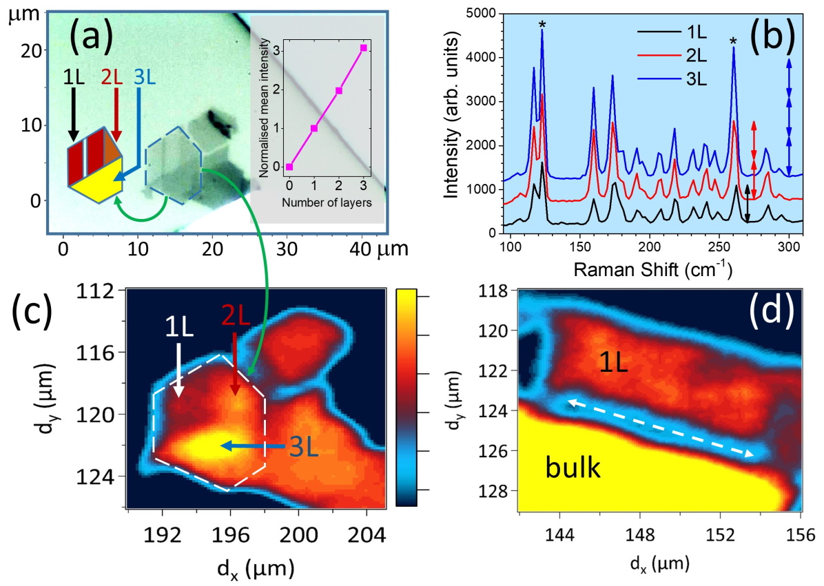
Studying the dependence of the physical properties of layered materials as a function of their thickness requires samples with well-established layer numbers down to one monolayer. This task is more challenging than usual for the rhenium-based TMDs since, to enable comparisons between different flakes, their crystallographic orientations must be established including, possibly, their vertical orientation [33, 34] as turning a flake upside-down is not a symmetry operation for ReSe2. We have overcome this problem by exfoliating large flakes which contain regions of different thicknesses as shown in Fig. 1 (see also Figs. S1 and S2). Fig. 1(a) shows an optical micrograph of a sample whose leftmost flake contains monolayer (1L), bilayer (2L) and trilayer (3L) regions, identified on the sketch to the left of the flake. All the regions derive from the same parent crystal and have preserved the same orientation as implied by the visible cleavage edges [35] at and and as confirmed rigorously by the Raman spectra of Fig. 1(b). Any significant rotation of one region with respect to the others would result in changes in the relative intensities of the different peaks within the spectrum due to the pronounced in-plane anisotropy of ReSe2 [28, 36, 33, 34]. The orientation of the flakes is supported by a reciprocal space map of photoemission intensity for the monolayer, shown in Fig. S3, which was recorded near the energy of the valence band maximum and displays the characteristic anisotropy already known from bulk ReSe2. We confirmed layer numbers by four independent means: Raman spectroscopy, scanning photoemission microscopy, AFM and nano-ARPES (AFM images and line scans for all samples are shown in Figs. S1 and S2). AFM step height measurements gave a monolayer thickness of 0.60 to 0.67 nm, comparable to the interlayer lattice parameter nm [37, 7] (note, the crystallographic axis in ReSe2 is tilted away from the normal to the layer). The thicknesses of the 2L and 3L regions were likewise confirmed by AFM (Fig. S2). Moreover, the Raman intensity from these regions scales linearly with the number of layers. This is best seen by looking at two Raman bands marked with asterisks in Fig. 1(b) which dominate the spectrum and do not overlap strongly with other spectral features – vertical arrows next to the peaks clearly indicate the scaling. We also fit and average areas of these peaks following subtraction of a small background and present the results in the inset of panel (a). Since the silicon substrate does not have a thick oxide layer, and because the ReSe2 layers were placed on a highly oriented pyrolytic graphite (HOPG) flake on the substrate, there is no modulation of the Raman intensity due to interference effects [38, 28]. The shifts in zone centre phonon frequencies with the number of layers are smaller for ReSe2 and ReS2 than for most TMDs [39, 28] so that, here, interference-free Raman intensities are more reliable than Raman peak shifts for determination of layer thicknesses. However, the measured Raman peak positions support our thickness assignments: the bulk modes at 283.6 and 260.5 cm-1 show a small shift to 285.2 and 263.0 cm-1 in the monolayer sample, in agreement with previous experimental and computational results [30].

Figs. 1(c) and (d) show maps of the photoemission intensity from the Re 4 core levels (binding energy 40-44 eV) from the sample of Fig. 1(a) and one other sample containing monolayer and bulk regions with the same orientation. These maps were recorded primarily to locate the different regions for the ARPES experiments. Interestingly, the contrast in photoelectron count from 1L to 3L regions reflects the layer thicknesses. The core level photoemission intensity need not necessarily depend linearly on the number of ReSe2 layers, but in principle it could be determined quantitatively by using X-ray photoelectron spectroscopy tools [40]. As Figs. 1(c) shows, discrimination between regions differing by one layer is possible and this mapping correlates with the Raman data. Imaging based on possible shifts in the energy of the Re 4 core levels [41], on the other hand, did not produce any contrast between the different regions.
III.2 ARPES results from atomically thin ReSe2
Because ReSe2 possesses only inversion symmetry, the Brillouin zone of the monolayer is a distorted regular hexagon and the and points form three non-equivalent pairs (, and their inversion equivalents). In this work, we consider only dispersions in two key directions: along, and normal to, the Re chains, for simplicity labeled and respectively; see Fig. 2(a) for the indication of these directions in the real and reciprocal spaces and (b) for comparison of the bulk and two-dimensional Brillouin zones of ReSe2 (the latter is a projection of the former along the reciprocal space axis). These special directions correspond to, for example, the polarization directions of the two band edge excitons in ReSe2 [42, 43, 44] and were identified as the directions of maximum and minimum dispersion in the studies of bulk material [23, 45]. We present the measured valence band dispersions for the monolayer (1L) flake shown in Fig. 1(d) in Fig. 2(c,e) for and (d,f) for . The right-hand panels in (c) and (d) show second derivatives with respect to energy of the data in the left, and in (e) and (f) we show expanded views of the same data and its second derivatives close to the valence band maximum (within eV). The extraordinarily flat nature of the top of the valence band in the direction is striking and is the main result of this work (Fig. 2(c,e)). As we show later, this is very different to the bulk valence band structure. By contrast, the top valence band remains dispersive in the near-orthogonal direction (Fig. 2(d,f)). Because second derivatives can occasionally generate spurious features, we have examined the energy distribution curves (EDCs) which are the raw data for Fig. 2, directly. Fig. S4 of the SM shows these EDCs in the and directions and confirms the flatness of the band along while the direction shows significant dispersion.
One more prominent feature of the 1L ReSe2 valence band structure is the locally flat band centred at at about 1 eV below the valence band edge (at a binding energy of 2 eV) which yields a particularly high photoemission intensity. This feature was shown to correspond to the valence band formed predominantly by the out-of-plane Re and Se orbitals [20]. Fig. 2 also shows the valence bands of the HOPG substrate on which the ReSe2 flakes were placed. The observation of the point of graphite (at ) usefully confirms the experimental location of the first Brillouin zone and point of the ReSe2 flakes and, as a result of the relatively large unit cell of ReSe2, the accessible momentum range allows us to sample almost two complete Brillouin zones in the direction. The data of Fig. 2 show no evidence for hybridization or appreciable opening of gaps at the binding energy and momentum values where the bands of ReSe2 and HOPG intersect. These results contrast with recently reported findings of strong coupling to graphene for TMDs such as WSe2 [46] and MoS2 [47] though, in those studies, the flakes also had graphene capping layers which the present samples did not.
III.3 Evolution of the valence band with the number of layers
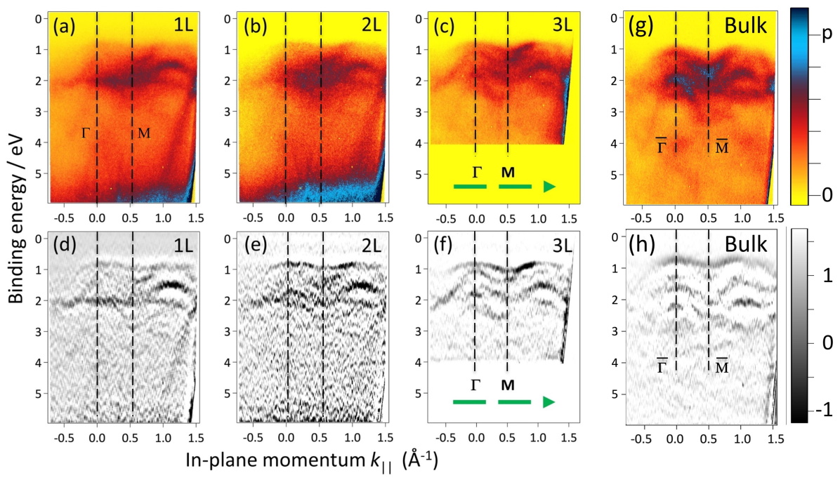
Following the discussion of the ARPES of the monolayer region shown in Fig. 1(d), we move to the flake presented in Fig. 1(a) and (c). Between the two samples, we can not only test the reproducibility of the 1L results of Fig. 2 as well as those for the bulk, but also study the evolution of the valence band states as a function of crystal thickness. In Fig. 3, we show photointensity as a function of binding energy and momentum, (a)-(c), and its second-derivative, (d)-(f), recorded using nano-ARPES for all our few-layer flakes as well as bulk,(g) and (h), for a momentum slice in the direction (note, the data in (c) and (f) was not recorded over the same binding energy range as in the other panels). For this comparison, we labelled the bands of the bulk flake following the high symmetry points of the projected 2D Brillouin zone, using symbols , and to indicate that the vertical momentum component of the bands is not specified (at the photon energy used here (100 eV), ARPES probes states lying in an approximately planar surface passing near the point at the top of the 3D Brillouin zone [23] shown in Fig. 2(b), i.e, ). Although the data for monolayer are not as clear as those obtained with the larger sample of Fig. 2, there is a systematic trend in the band width of the uppermost valence band.
We use our raw data to obtain the width of that band - we extract photoemission counts as a function of binding energy (that is, the energy distribution curves, EDCs) and fit these to obtain a measure of the band edge position at each momentum along the and directions. This, in turn, allows us to identify the energies of the band extrema. The results of our procedure (for further details of the fitting process see the SM, Figs. S5 and S6) are shown in Fig. 4(a), where we compare the extracted top valence bands for 1L, 2L, 3L and bulk. The curves for 2L, 3L and bulk are shifted vertically by steps of 0.4 eV for clarity (the same shift is applied to and in each case). The corresponding raw data are shown in the SM, Figs. S7-S9 (in Fig. S11 we show a comparison of the raw data with the calculated band structures of bulk and monolayer samples in the and directions). A summary of the band widths obtained from fitting the EDCs is displayed in Fig. 4(b) which illustrates flattening of the top valence band along with decreasing crystal thickness while the band width along is comparable for three out of four investigated sample thicknesses. The error bars are estimated from the sensitivity of the measured band width to variation of the fitting parameters (principally the threshold intensity corresponding to the band edge; see Fig. S6 for a definition of ). The error for the case of the bilayer in the direction is somewhat larger as the data is slightly poorer (see Fig. S8); the 2L region was the smallest of the flakes (see Fig. 1(a)) and therefore the most difficult to measure. Note, band width values in the bulk case are photon energy-dependent due to the dispersion normal to the layers; our present values agree well with previous values measured on cleaner, cleaved bulk material [23] at the same photon energy.
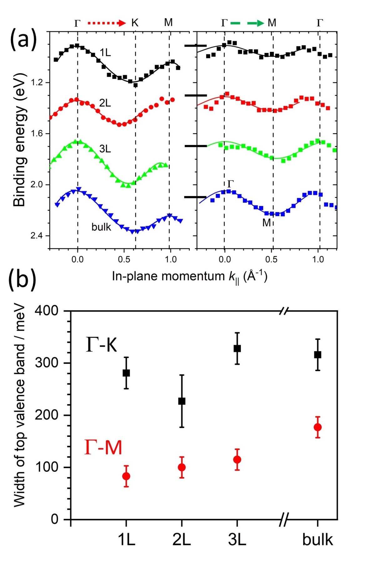
Our experimental findings are also supported by density functional theory (DFT) calculations. Using scalar relativistic pseudopotentials, we obtained band widths of 95 meV (1L), 150 meV (2L), 275 meV (3L) and 500 meV for bulk. A fully relativistic calculation yielded similar values of 85, 187, 217 and 436 meV, respectively. The calculated band structures along the direction are shown in section S4 of the SM (Fig. S10) and the trend in their variation as a function of crystal thickness agrees well with the measurements.
At the photon energy of 100 eV used here for the nano-ARPES experiments, the recorded signal is highly surface-specific: the predicted inelastic mean free path of MoS2, for example, ranges from 3.5 to 6.0 Å for photon energies from 70 to 170 eV respectively, [48, 49, 50] comparable to the layer thickness of ReSe2 (-axis 6.7 Å), and a simple estimate based on the universal curve [51] gives 5.5 Å at 100 eV. Despite this, Fig. 3 and Fig. 4 demonstrate systematic changes in the valence band edge as a function of the number of layers. Overall, our nano-ARPES data reveals valence band states that are clearly dependent on inter-layer hopping interactions and must be representative of the body of the flake. We do not observe electronic states confined to individual layers except in the case of the 1L sample itself. This is in agreement with studies of bulk and few-layer ReS2 [52, 53]. Thus, although the inter-layer interactions of ReSe2 are weak, very similar to ReS2 [39, 30] (which shows a higher inter-layer resistivity than typical TMDs [54]), they are certainly non-negligible [55]. To compare, the interlayer coupling-induced dispersion of the highest valence band for in bulk ReSe2 is 100 meV [23] while it is 800 meV in MoSe2 and 1 eV in MoS2 [56].
Recently, the surface-sensitivity of ARPES has been applied to reveal hidden spin polarisation [57] in centrosymmetric bulk TMDs, for example, WSe2 [58, 59], MoS2 [60], NbSe2 [61], and PtSe2 [62]. In the nomenclature of spin-polarisation effects introduced by Zhang et al. [57], D-1 signifies a spin polarization arising from conventional bulk Dresselhaus inversion asymmetry and D-2 implies localised Dresselhaus spin polarizations compensated by their opposites under bulk inversion symmetry. The case of MoS2 was considered theoretically [63]; -MoS2 is a system where individual D-1 layers interact (weakly) to give D-2 behaviour in bulk. Surface-sensitive techniques such as STM or ARPES can probe the top layer of a bulk crystal and can reveal its D-1 nature. However, once again, ReX2 proves to be an untypical member of the TMD family, because its structure contains a centre of inversion at the midpoint of each diamond of four Re atoms. On symmetry grounds, therefore, even a monolayer is only expected to show D-2 behaviour. The opposing spin polarisations reside on Re atoms located close to one another in the same layer, meaning that the near single-layer sensitivity of ARPES cannot resolve individual D-1 contributions. This is borne out by the lack of observed spin-orbit splittings here or in any earlier ARPES data on bulk or few-layer ReX2 [20, 64, 52, 53, 23, 45].
III.4 In-plane anisotropy and interlayer coupling
In order to understand better the anisotropic change in the band width of the top valence band as a function of the number of layers, we investigated the orbital character of the valence band of monolayer and bulk ReSe2 using density functional theory calculations and show the key results for monolayer in Fig. 5 (the complete set of projections for the monolayer as well as bulk are presented in Section S4 of the SM). In these calculations, we have neglected the spin-orbit coupling so that the atomic wavefunctions are purely orbital angular momentum states (this is acceptable because inversion symmetry which forbids any band spin splitting is present for all crystal thicknesses, even monolayer). For this discussion, are defined as the directions along and normal to the Re chains respectively and is normal to the layer, as in Fig. 5(a).
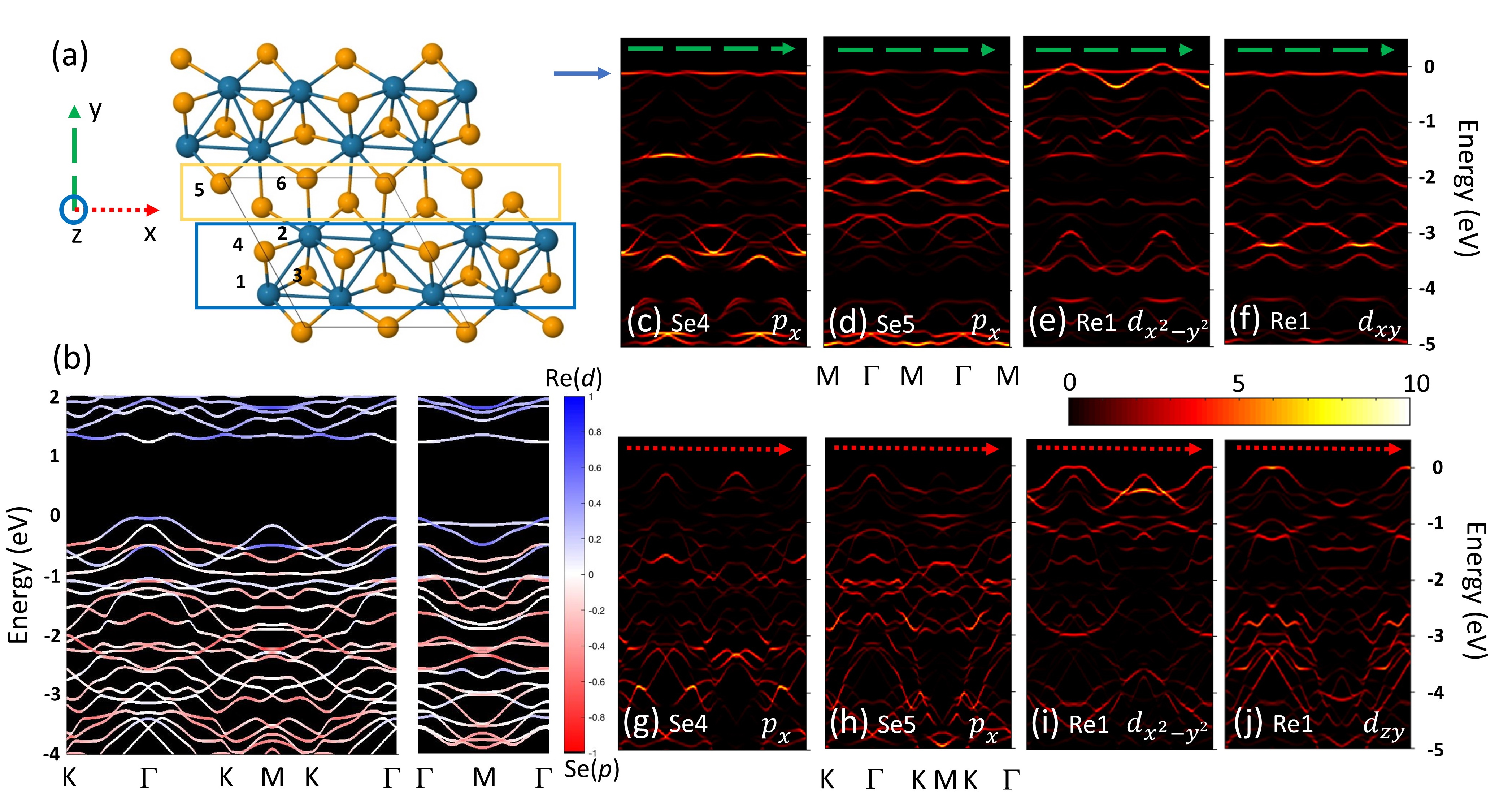
In Fig. 5(b), we show the valence band dispersion of monolayer ReSe2 along the directions and (calculated at the scalar relativistic GGA level) projected onto Se and Re orbitals with the respective amplitudes shown using red and blue false color scales and white indicating an equal admixture. In general, the Re states dominate in the conduction bands while the Se orbitals prevail on the valence band side. However, the top valence band defies this simple picture: states in the vicinity of are built mainly of the Re orbitals while those around of Se orbitals. Along , the Re -character band forming the valence band maximum around crosses the second band made of a mixture of Re - and Se -orbitals so that the highest energy states in this direction contain comparable transition metal and chalcogen contributions. We suggest it is this difference between the orbital composition of the top valence band in the directions along () and perpendicular () to the rhenium chains that leads to the unique coupling between in-plane anisotropy of this band and the crystal thickness. The sandwich-like nature of TMD monolayers means that chalcogen orbitals are more involved in, and hence affected by, the interlayer interaction than the rhenium orbitals. Hence, while states in the direction are significantly affected by the presence of other layers in thicker crystals which is reflected by the growing dispersion in Fig. 4(b), only a small part of states along responds to interlayer coupling so that the band width in this direction remains similar in flakes of different thicknesses. In a sense, this mechanism is similar to the one driving the direct-indirect band gap transition in 2H TMDs like MoS2 [12, 13, 14] where interlayer coupling causes shifts of the highest valence band in the vicinity of (made of out-of-plane S and Mo orbitals) while the states around (formed by in-plane Mo -orbitals) remain unaffected. In ReSe2 however, out-of-plane orbitals do not contribute to the highest valence band and so the distinction is rather between the atomic species than orbital symmetries.
We investigate the orbital contributions of Re and Se to the valence band in more detail in Fig. 5(c)-(j). We note that the four selenium sites that are not related by symmetry make different contributions to the band structure and, of these, one can identify two main types of chalcogen site: those located on the Re diamonds, labeled atoms 3 and 4 in Fig. 5(a), and those bridging adjacent Re chains (atoms 5 and 6) which differ markedly. Evidence for the non-equivalence of these sites is also provided by Raman spectroscopy studies of ReSe2-xSx alloys which showed that the substitution of sulphur on the different chalcogen sites yields different formation energies and vibrational frequencies [23] whilst high resolution electron microscopy suggests preferential occupation of the more stable sites by impurities [65]. Scanning tunneling microscopy (STM) and spectroscopy (STS) likewise show very clearly the non-equivalence of the four selenium sites in ReSe2 [66]. The projections of the valence band states onto the Se orbitals, Fig. 5(c) and (d), show that it is the orbitals of Se sites 4 (and 3, see Fig. S15) that contribute to the flat VBM in the direction. As seen in Fig. 5(d) and (h), the contribution of Se of sites 5 (and 6, Fig. S15) to the valence band edge is less significant. From the coordinate system shown in Fig. 5(a), it is clear that the states of sites 3 and 4 are polarized along the Re chains and are spatially localized above and below them. The interaction between the orbitals of Se sites 3 and 4 on neighboring chains is minimal and this gives rise to a near-absence of dispersion in the () direction in the monolayer. The dispersion along the () direction is generated predominantly by Re and orbitals, Fig. 5(i) and (j).
IV Summary
We have demonstrated that in ReSe2 in-plane anisotropy is quite uniquely coupled to interlayer interaction so that decreasing the number of layers in the crystal decreases the dispersion in the direction perpendicular to the rhenium chains ( in reciprocal space). This implies increasing interchain decoupling and a growing one-dimensional character of electronic states in this material. The extremely flat valence band dispersion perpendicular to the Re chains implies that, in monolayer ReSe2, hole transport should be dominated by conduction along the direction of the Re chains and thus should be extremely anisotropic. No experimental test of this has yet been carried out, though it is established that the in-plane mobility is lowest perpendicular to the Re chains in bulk-like material. An anisotropy of about a factor of two between mobilities in the and directions was reported for few-layer ReSe2-xSx devices [67] but their reported number of layers was which, as shown above, is too thick to observe the present effects; furthermore, they observed -type conductivity. Another study found an anisotropy ratio of for -type conductivity in W-doped bulk material [68] in agreement with a recent ARPES study [69]. Several other studies on exfoliated material likewise used few-layer flakes down to 3L, or -type material, and so do not provide a test of the present predictions [70, 71, 72, 73, 74]. There is only one report of measurements on -type conductivity in a monolayer, where a hole mobility of 10 cm2V-1s-1 was found, but the anisotropy of the charge transport was apparently not investigated [74]. It is therefore a high priority to investigate transport in monolayer ReSe2 in suitably designed structures which would ideally allow for investigation both of the predicted anisotropy but also electrostatic gating to ensure hole transport dominates. The quasi-one dimensional nature of hole transport in ReSe2 offers the possibility of a momentum-selective filter or contact to other TMD layers in either lateral or vertical heterostructures.
Acknowledgements.
This work was supported by the Centre for Graphene Science of the Universities of Bath and Exeter and by the EPSRC (UK) under grants EP/G036101, EP/M022188, and EP/P004830; L.S.H. and S.M.G. are supported by the Bath/Bristol Centre for Doctoral Training in Condensed Matter Physics, EPSRC grant EP/L015544. M.M-K. acknowledges support from the University of Bath International Funding Scheme. We thank the SOLEIL synchrotron for the provision of beam time; work at SOLEIL was supported by EPSRC grant EP/P004830/1. The present collaborative research was undertaken in the context of the Associated Unit MATINÉE of the Spanish Scientific Research Council (CSIC). Computational work was performed on the University of Bath’s High Performance Computing Facility. Data created during this research are freely available from the University of Bath data archive at DOI:10.15125/BATH-00521.References
- Bahramy et al. [2018] M. Bahramy, O. Clark, B.-J. Yang, J. Feng, L. Bawden, J. Riley, I. Marković, F. Mazzola, V. Sunko, and D. Biswas, Ubiquitous formation of bulk Dirac cones and topological surface states from a single orbital manifold in transition-metal dichalcogenides, Nature Materials 17, 21 (2018).
- Mak and Shan [2016] K. F. Mak and J. Shan, Photonics and optoelectronics of 2D semiconductor transition metal dichalcogenides, Nature Photonics 10, 216 (2016).
- Wang et al. [2012] Q. H. Wang, K. Kalantar-Zadeh, A. Kis, J. N. Coleman, and M. S. Strano, Electronics and optoelectronics of two-dimensional transition metal dichalcogenides, Nature Nanotechnology 7, 699 (2012).
- Nayak et al. [2017] P. K. Nayak, Y. Horbatenko, S. Ahn, G. Kim, J.-U. Lee, K. Y. Ma, A. R. Jang, H. Lim, D. Kim, S. Ryu, H. Cheong, N. Park, and H. S. Shin, Probing evolution of twist-angle-dependent interlayer excitons in MoSe2/WSe2 van der Waals heterostructures, ACS Nano 11, 4041 (2017).
- He et al. [2016] Y. He, Y. Yang, Z. Zhang, Y. Gong, W. Zhou, Z. Hu, G. Ye, X. Zhang, E. Bianco, S. Lei, Z. Jin, X. Zou, Y. Yang, Y. Zhang, E. Xie, J. Lou, B. Yakobson, R. Vajtai, B. Li, and P. Ajayan, Strain-induced electronic structure changes in stacked van der Waals heterostructures, Nano Letters 16, 3314 (2016).
- Li et al. [2016] Y. Li, K.-A. N. Duerloo, K. Wauson, and E. J. Reed, Structural semiconductor-to-semimetal phase transition in two-dimensional materials induced by electrostatic gating, Nature Communications 7, 10671 (2016).
- Lamfers et al. [1996] H.-J. Lamfers, A. Meetsma, G. Wiegers, and J. de Boer, The crystal structure of some rhenium and technetium dichalcogenides, Journal of Alloys and Compounds 241, 34 (1996).
- Rahman et al. [2017] M. Rahman, K. Davey, and S.-Z. Qiao, Advent of 2D rhenium disulfide (ReS2): Fundamentals to applications, Advanced Functional Materials 27, 1606129 (2017).
- Wang et al. [2016] L. Wang, Z. Sofer, J. Luxa, D. Sedmidubský, A. Ambrosi, and M. Pumera, Layered rhenium sulfide on free-standing three-dimensional electrodes is highly catalytic for the hydrogen evolution reaction: Experimental and theoretical study, Electrochemistry Communications 63, 39 (2016).
- Aliaga et al. [2017] J. A. Aliaga, T. Zepeda, J. F. Araya, F. Paraguay-Delgado, E. Benavente, G. Alonso-Núñez, S. Fuentes, and G. González, Low-dimensional ReS2/C composite as effective hydrodesulfurization catalyst, Catalysts 7, 377 (2017).
- Zhao et al. [2018] H. Zhao, Z. Dai, X. Xu, J. Pan, and J. Hu, Integrating semiconducting catalyst of ReS2 nanosheets into p-silicon photocathode for enhanced solar water reduction, ACS Applied Materials & Interfaces 10, 23074 (2018).
- Splendiani et al. [2010] A. Splendiani, L. Sun, Y. Zhang, T. Li, J. Kim, C.-Y. Chim, G. Galli, and F. Wang, Emerging photoluminescence in monolayer MoS2, Nano Letters 10, 1271 (2010).
- Jin et al. [2013] W. Jin, P.-C. Yeh, N. Zaki, D. Zhang, J. T. Sadowski, A. Al-Mahboob, A. M. van Der Zande, D. A. Chenet, J. I. Dadap, I. P. Herman, P. Sutter, J. Hone, and R. M. Osgood Jr., Direct measurement of the thickness-dependent electronic band structure of MoS2 using angle-resolved photoemission spectroscopy, Physical Review Letters 111, 106801 (2013).
- Zhang et al. [2014a] Y. Zhang, T.-R. Chang, B. Zhou, Y.-T. Cui, H. Yan, Z. Liu, F. Schmitt, J. Lee, R. Moore, Y. Chen, H. Lin, H.-T. Jeng, S.-K. Mo, Z. Hussain, A. Bansil, and Z.-X. Shen, Direct observation of the transition from indirect to direct bandgap in atomically thin epitaxial MoSe2, Nature Nanotechnology 9, 111 (2014a).
- Jung et al. [2015] C. S. Jung, F. Shojaei, K. Park, J. Y. Oh, H. S. Im, D. M. Jang, J. Park, and H. S. Kang, Red-to-ultraviolet emission tuning of two-dimensional gallium sulfide/selenide, ACS Nano 9, 9585 (2015).
- Ben Aziza et al. [2017] Z. Ben Aziza, D. Pierucci, H. Henck, M. G. Silly, C. David, M. Yoon, F. Sirotti, K. Xiao, M. Eddrief, J.-C. Girard, and A. Ouerghi, Tunable quasiparticle band gap in few-layer GaSe/graphene van der Waals heterostructures, Physical Review B 96, 035407 (2017).
- Hamer et al. [2019] M. J. Hamer, J. Zultak, A. V. Tyurnina, V. Zólyomi, D. Terry, A. Barinov, A. Garner, J. Donoghue, A. P. Rooney, V. Kandyba, A. Giampietri, A. Graham, N. Teutsch, X. Xia, M. Koperski, S. J. Haigh, V. I. Fal’ko, R. V. Gorbachev, and N. R. Wilson, Indirect to direct gap crossover in two-dimensional InSe revealed by angle-resolved photoemission spectroscopy, ACS Nano 13, 2136 (2019).
- Yuan et al. [2015] H. Yuan, X. Liu, F. Afshinmanesh, W. Li, G. Xu, J. Sun, B. Lian, A. G. Curto, G. Ye, Y. Hikita, Z. Shen, S.-C. Zhang, X. Chen, M. Brongersma, H. Y. Hwang, and Y. Cui, Polarization-sensitive broadband photodetector using a black phosphorus vertical p–n junction, Nature Nanotechnology 10, 707 (2015).
- Kertesz and Hoffmann [1984] M. Kertesz and R. Hoffmann, Octahedral vs trigonal-prismatic coordination and clustering in transition-metal dichalcogenides, Journal of the American Chemical Society 106, 3453 (1984).
- Choi et al. [2020] B. K. Choi, S. Ulstrup, S. M. Gunasekera, J. Kim, S. Y. Lim, L. Moreschini, J. S. Oh, S.-H. Chun, C. Jozwiak, A. Bostwick, E. Rotenberg, H. Cheong, I.-W. Lyo, M. Mucha-Kruczynski, and Y. J. Chang, Visualizing orbital content of electronic bands in anisotropic 2D semiconducting ReSe2, ACS Nano 14, 7880 (2020).
- [21] See Supplemental Material at URL for optical and AFM images of monolayer and few-layer flakes; photoemission energy distribution curves for monolayer ReSe2; calculated VB dispersion in the direction for few-layer and bulk ReSe2; measured VB dispersions of few-layer ReSe2 and their second derivatives; comparison of calculated and experimental dispersions of ReSe2; projections of calculated VB dispersion onto Se - and Re -orbitals in and directions.
- Yeh and Lindau [1985] J. J. Yeh and I. Lindau, Atomic subshell photoionization cross sections and asymmetry parameters: , Atomic Data and Nuclear Data Tables 32, 1 (1985).
- Hart et al. [2017] L. S. Hart, J. L. Webb, S. Dale, S. J. Bending, M. Mucha-Kruczynski, D. Wolverson, C. Chen, J. Avila, and M. C. Asensio, Electronic bandstructure and van der waals coupling of ReSe2 revealed by high-resolution angle-resolved photoemission spectroscopy, Scientific Reports 7, 5145 (2017).
- Giannozzi et al. [2009] P. Giannozzi, S. Baroni, N. Bonini, M. Calandra, R. Car, C. Cavazzoni, D. Ceresoli, G. L. Chiarotti, M. Cococcioni, I. Dabo, A. Dal Corso, S. de Gironcoli, S. Fabris, G. Fratesi, R. Gebauer, U. Gerstmann, C. Gougoussis, A. Kokalj, M. Lazzeri, L. Martin-Samos, N. Marzari, F. Mauri, R. Mazzarello, S. Paolini, A. Pasquarello, L. Paulatto, C. Sbraccia, S. Scandolo, G. Sclauzero, A. P. Seitsonen, A. Smogunov, P. Umari, and R. M. Wentzcovitch, QUANTUM ESPRESSO: a modular and open-source software project for quantum simulations of materials, Journal of Physics: Condensed Matter 21, 395502 (2009).
- Blöchl [1994] P. E. Blöchl, Projector augmented-wave method, Physical Review B 50, 17953 (1994).
- Kresse and Joubert [1999] G. Kresse and D. Joubert, From ultrasoft pseudopotentials to the projector augmented-wave method, Physical Review B 59, 1758 (1999).
- Monkhorst and Pack [1976] H. J. Monkhorst and J. D. Pack, Special points for brillouin-zone integrations, Physical Review B 13, 5188 (1976).
- Wolverson et al. [2014] D. Wolverson, S. Crampin, A. S. Kazemi, A. Ilie, and S. J. Bending, Raman spectra of monolayer, few-layer, and bulk ReSe2: An anisotropic layered semiconductor, ACS Nano 8, 11154 (2014).
- Gunasekera et al. [2018] S. M. Gunasekera, D. Wolverson, L. S. Hart, and M. Mucha-Kruczynski, Electronic band structure of rhenium dichalcogenides, Journal of Electronic Materials 47, 4314 (2018).
- Zhao et al. [2015] H. Zhao, J. Wu, H. Zhong, Q. Guo, X. Wang, F. Xia, L. Yang, P. Tan, and H. Wang, Interlayer interactions in anisotropic atomically thin rhenium diselenide, Nano Research 8, 3651 (2015).
- Zhong et al. [2015] H.-X. Zhong, S. Gao, J.-J. Shi, and L. Yang, Quasiparticle band gaps, excitonic effects, and anisotropic optical properties of the monolayer distorted diamond-chain structures ReS2 and ReSe2, Physical Review B 92, 115438 (2015).
- Grimme et al. [2010] S. Grimme, J. Antony, S. Ehrlich, and H. Krieg, A consistent and accurate ab initio parametrization of density functional dispersion correction (dft-d) for the 94 elements h-pu, J. Chem. Phys. 132, 154104 (2010).
- Hart et al. [2016] L. Hart, S. Dale, S. Hoye, J. L. Webb, and D. Wolverson, Rhenium dichalcogenides: layered semiconductors with two vertical orientations, Nano Letters 16, 1381 (2016).
- McCreary et al. [2017] A. McCreary, J. R. Simpson, Y. Wang, D. Rhodes, K. Fujisawa, L. Balicas, M. Dubey, V. H. Crespi, M. Terrones, and A. R. Hight Walker, Intricate resonant raman response in anisotropic res2, Nano Letters 17, 5897 (2017).
- Liu et al. [2015] E. Liu, Y. Fu, Y. Wang, Y. Feng, H. Liu, X. Wan, W. Zhou, B. Wang, L. Shao, C.-H. Ho, Y.-S. Huang, Z. Cao, L. Wang, A. Li, J. Zeng, F. Song, X. Wang, Y. Shi, H. Yuan, H. Y. Hwang, Y. Cui, F. Miao, and D. Xing, Integrated digital inverters based on two-dimensional anisotropic ReS2 field-effect transistors, Nature Communications 6, 6991 (2015).
- Chenet et al. [2015] D. A. Chenet, O. B. Aslan, P. Y. Huang, C. Fan, A. M. van der Zande, T. F. Heinz, and J. C. Hone, In-plane anisotropy in mono- and few-layer ReS2 probed by raman spectroscopy and scanning transmission electron microscopy, Nano Letters 15, 5667 (2015).
- Jariwala et al. [2016] B. Jariwala, A. Thamizhavel, and A. Bhattacharya, ReSe2: a reassessment of crystal structure and thermal analysis, Journal of Physics D: Applied Physics 50, 044001 (2016).
- Blake et al. [2007] P. Blake, E. Hill, A. Castro Neto, K. Novoselov, D. Jiang, R. Yang, T. Booth, and A. Geim, Making graphene visible, Applied Physics Letters 91, 063124 (2007).
- Tongay et al. [2014] S. Tongay, H. Sahin, C. Ko, A. Luce, W. Fan, K. Liu, J. Zhou, Y.-S. Huang, C.-H. Ho, J. Yan, D. F. Ogletree, S. Aloni, J. Ji, S. Li, J. Li, F. M. Peeters, and J. Wu, Monolayer behaviour in bulk ReS2 due to electronic and vibrational decoupling, Nature Communications 5, 3252 (2014).
- Smekal et al. [2005] W. Smekal, W. S. M. Werner, and C. J. Powell, Simulation of electron spectra for surface analysis (SESSA): a novel software tool for quantitative Auger-electron spectroscopy and X-ray photoelectron spectroscopy, Surface and Interface Analysis 37, 1059 (2005).
- Ho et al. [1999] C. Ho, Y. Huang, J. Chen, T. Dann, and K. Tiong, Electronic structure of ReS2 and ReSe2 from first-principles calculations, photoelectron spectroscopy, and electrolyte electroreflectance, Physical Review B 60, 15766 (1999).
- Ho et al. [1998] C. H. Ho, Y. S. Huang, K. K. Tiong, and P. C. Liao, Absorption-edge anisotropy in and layered semiconductors, Physical Review B 58, 16130 (1998).
- Ho et al. [2004] C.-H. Ho, H. Lee, and C. Wu, Polarization sensitive behaviour of the band-edge transitions in ReS2 and ReSe2 layered semiconductors, Journal of Physics: Condensed Matter 16, 5937 (2004).
- Ho et al. [2007] C. Ho, M. Hsieh, C. Wu, Y. Huang, and K. Tiong, Dichroic optical and electrical properties of rhenium dichalcogenides layer compounds, Journal of Alloys and Compounds 442, 245 (2007).
- Eickholt et al. [2018] P. Eickholt, J. Noky, E. Schwier, K. Shimada, K. Miyamoto, T. Okuda, C. Datzer, M. Drüppel, P. Krüger, M. Rohlfing, and M. Donath, Location of the valence band maximum in the band structure of anisotropic 1T’- ReSe2, Physical Review B 97, 165130 (2018).
- Wilson et al. [2017] N. R. Wilson, P. V. Nguyen, K. Seyler, P. Rivera, A. J. Marsden, Z. P. L. Laker, G. C. Constantinescu, V. Kandyba, A. Barinov, N. D. M. Hine, X. Xu, and D. H. Cobden, Determination of band offsets, hybridization, and exciton binding in 2D semiconductor heterostructures, Science Advances 3, e1601832 (2017).
- Coy Diaz et al. [2015] H. Coy Diaz, J. Avila, C. Chen, R. Addou, M. C. Asensio, and M. Batzill, Direct observation of interlayer hybridization and Dirac relativistic carriers in graphene/MoS2 van der Waals heterostructures, Nano Letters 15, 1135 (2015).
- Han et al. [2012] S. W. Han, G.-B. Cha, E. Frantzeskakis, I. Razado-Colambo, J. Avila, Y. S. Park, D. Kim, J. Hwang, J. S. Kang, S. Ryu, W. S. Yun, S. C. Hong, and M. C. Asensio, Band-gap expansion in the surface-localized electronic structure of MoS2(0002), Physical Review B 86, 115105 (2012).
- Lince et al. [1989] J. R. Lince, T. B. Stewart, M. M. Hills, P. D. Fleischauer, J. A. Yarmoff, and A. Taleb-Ibrahimi, Chemical effects of Ne+ bombardment on the MoS2(0001) surface studied by high-resolution photoelectron spectroscopy, Surface Science 210, 387 (1989).
- Tanuma et al. [1987] S. Tanuma, C. J. Powell, and D. R. Penn, Proposed formula for electron inelastic mean free paths based on calculations for 31 materials, Surface Science 192, L849 (1987).
- Seah and Dench [1979] M. P. Seah and W. A. Dench, Quantitative electron spectroscopy of surfaces: A standard data base for electron inelastic mean free paths in solids, Surface and Interface Analysis 1, 2 (1979).
- Biswas et al. [2017] D. Biswas, A. M. Ganose, R. Yano, J. Riley, L. Bawden, O. Clark, J. Feng, L. Collins-Mcintyre, M. Sajjad, W. Meevasana, T. K. Kim, M. Hoesch, J. E. Rault, T. Sasagawa, D. O. Scanlon, and P. D. C. King, Narrow-band anisotropic electronic structure of ReS2, Physical Review B 96, 085205 (2017).
- Gehlmann et al. [2017] M. Gehlmann, I. Aguilera, G. Bihlmayer, S. Nemšák, P. Nagler, P. Gospodarič, G. Zamborlini, M. Eschbach, V. Feyer, F. Kronast, E. Młynczak, T. Korn, L. Plucinski, C. Schüller, S. Blügel, and C. M. Schneider, Direct observation of the band gap transition in atomically thin ReS2, Nano Letters 17, 5187 (2017).
- Lee et al. [2019] B. C. Lee, J. Na, J. H. Choi, H. Ji, G.-T. Kim, and M.-K. Joo, Probing distinctive electron conduction in multilayer rhenium disulfide, Advanced Materials 31, 1805860 (2019).
- Echeverry and Gerber [2018] J. Echeverry and I. Gerber, Theoretical investigations of the anisotropic optical properties of distorted 1T-ReS2 and ReSe2 monolayers, bilayers, and in the bulk limit, Physical Review B 97, 075123 (2018).
- Böker et al. [2001] T. Böker, R. Severin, A. Müller, C. Janowitz, R. Manzke, D. Voß, P. Krüger, A. Mazur, and J. Pollmann, Band structure of and angle-resolved photoelectron spectroscopy and ab initio calculations, Phys. Rev. B 64, 235305 (2001).
- Zhang et al. [2014b] X. Zhang, Q. Liu, J.-W. Luo, A. J. Freeman, and A. Zunger, Hidden spin polarization in inversion-symmetric bulk crystals, Nature Physics 10, 387 (2014b).
- Riley et al. [2014] J. M. Riley, F. Mazzola, M. Dendzik, M. Michiardi, T. Takayama, L. Bawden, C. Granerød, M. Leandersson, T. Balasubramanian, M. Hoesch, T. K. Kim, H. Takagi, W. Meevasana, P. Hofmann, M. S. Bahramy, J. W. Wells, and P. D. C. King, Direct observation of spin-polarized bulk bands in an inversion-symmetric semiconductor, Nature Physics 10, 835 (2014).
- Bertoni et al. [2016] R. Bertoni, C. W. Nicholson, L. Waldecker, H. Hübener, C. Monney, U. De Giovannini, M. Puppin, M. Hoesch, E. Springate, and R. T. Chapman, Generation and evolution of spin-, valley-, and layer-polarized excited carriers in inversion-symmetric WSe2, Physical Review Letters 117, 277201 (2016).
- Gehlmann et al. [2016] M. Gehlmann, I. Aguilera, G. Bihlmayer, E. Młyńczak, M. Eschbach, S. Döring, P. Gospodarič, S. Cramm, B. Kardynał, L. Plucinski, S. Blügel, and C. M. Schneider, Quasi 2D electronic states with high spin-polarization in centrosymmetric MoS2 bulk crystals, Scientific Reports 6, 26197 (2016).
- Bawden et al. [2016] L. Bawden, S. Cooil, F. Mazzola, J. Riley, L. Collins-McIntyre, V. Sunko, K. Hunvik, M. Leandersson, C. Polley, and T. Balasubramanian, Spin-valley locking in the normal state of a transition-metal dichalcogenide superconductor, Nature Communications 7, 11711 (2016).
- Yao et al. [2017] W. Yao, E. Wang, H. Huang, K. Deng, M. Yan, K. Zhang, K. Miyamoto, T. Okuda, L. Li, Y. Wang, H. Gao, C. Liu, W. Duan, and S. Zhou, Direct observation of spin-layer locking by local Rashba effect in monolayer semiconducting PtSe2 film, Nature Communications 8, 14216 (2017).
- Liu et al. [2015] Q. Liu, X. Zhang, H. Jin, K. Lam, J. Im, A. J. Freeman, and A. Zunger, Search and design of nonmagnetic centrosymmetric layered crystals with large local spin polarization, Physical Review B 91, 235204 (2015).
- Webb et al. [2017] J. L. Webb, L. S. Hart, D. Wolverson, C. Chen, J. Avila, and M. C. Asensio, Electronic band structure of ReS2 by high-resolution angle-resolved photoemission spectroscopy, Physical Review B 96, 115205 (2017).
- Wen et al. [2017] W. Wen, J. Lin, K. Suenaga, Y. Guo, Y. Zhu, H.-P. Hsu, and L. Xie, Preferential S/Se occupation in an anisotropic ReS2-xSe2x monolayer alloy, Nanoscale 9, 18275 (2017).
- Hong et al. [2018] M. Hong, X. Zhou, N. Gao, S. Jiang, C. Xie, L. Zhao, Y. Gao, Z. Zhang, P. Yang, Y. Shi, Q. Zhang, Z. Liu, J. Zhao, and Y. Zhang, Identifying the non-identical outermost selenium atoms and invariable band gaps across the grain boundary of anisotropic rhenium diselenide, ACS Nano 12, 10095 (2018).
- Liu et al. [2016] F. C. Liu, S. J. Zheng, A. Chaturvedi, V. Zolyomi, J. D. Zhou, Q. D. Fu, C. Zhu, P. Yu, Q. S. Zeng, N. D. Drummond, H. J. Fan, C. Kloc, V. I. Fal’ko, X. X. He, and Z. Liu, Optoelectronic properties of atomically thin ReSSe with weak interlayer coupling, Nanoscale 8, 5826 (2016).
- Hu et al. [2006] S. Hu, C. Liang, K. Tiong, Y. Huang, and Y. Lee, Electrical anisotropy of W-doped ReSe2 crystals, Journal of The Electrochemical Society 153, J100 (2006).
- Kim et al. [2019] B. S. Kim, W. S. Kyung, J. D. Denlinger, C. Kim, and S. R. Park, Strong one-dimensional characteristics of hole-carriers in ReS2 and ReSe2, Scientific Reports 9, 2730 (2019).
- Corbet et al. [2015] C. M. Corbet, C. McClellan, A. Rai, S. S. Sonde, E. Tutuc, and S. K. Banerjee, Field effect transistors with current saturation and voltage gain in ultrathin ReS2, ACS Nano 9, 363 (2015).
- Ali et al. [2018] M. H. Ali, D.-H. Kang, and J.-H. Park, Rhenium diselenide (ReSe2) infrared photodetector enhanced by (3-aminopropyl) trimethoxysilane (APTMS) treatment, Organic Electronics 53, 14 (2018).
- Zhang et al. [2016] E. Zhang, P. Wang, Z. Li, H. Wang, C. Song, C. Huang, Z.-G. Chen, L. Yang, K. Zhang, S. Lu, W. Wang, S. Liu, H. Fang, X. Zhou, H. Yan, J. Zou, X. Wan, P. Zhou, W. Hu, and F. Xiu, Tunable ambipolar polarization-sensitive photodetectors based on high-anisotropy ReSe2 nanosheets, ACS Nano 10, 8067 (2016).
- Yang et al. [2014a] S. Yang, S. Tongay, Q. Yue, Y. Li, B. Li, and F. Lu, High-performance few-layer Mo-doped ReSe2 nanosheet photodetectors, Scientific Reports 4, 5442 (2014a).
- Yang et al. [2014b] S. Yang, S. Tongay, Y. Li, Q. Yue, J.-B. Xia, S.-S. Li, J. Li, and S.-H. Wei, Layer-dependent electrical and optoelectronic responses of ReSe2 nanosheet transistors, Nanoscale 6, 7226 (2014b).