Sorting in Memristive Memory
Abstract.
Sorting data is needed in many application domains. Traditionally, the data is read from memory and sent to a general-purpose processor or application-specific hardware for sorting. The sorted data is then written back to the memory. Reading/writing data from/to memory and transferring data between memory and processing unit incur significant latency and energy overhead. In this work, we develop the first architectures for in-memory sorting of data to the best of our knowledge. We propose two architectures. The first architecture is applicable to the conventional format of representing data, i.e., weighted binary radix. The second architecture is proposed for developing unary processing systems, where data is encoded as uniform unary bit-streams. As we present, each of the two architectures has different advantages and disadvantages, making one or the other more suitable for a specific application. However, the common property of both is a significant reduction in the processing time compared to prior sorting designs. Our evaluations show on average 37 and 138 energy reduction for binary and unary designs, respectively, compared to conventional CMOS off-memory sorting systems in a 45nm technology. We designed a and a Median filter using the proposed sorting solutions, which we used for processing pixel images. Our results show a reduction of 14 and 634 in energy and latency, respectively, with the proposed binary, and 5.6 and 152 in energy and latency with the proposed unary approach compared to those of the off-memory binary and unary designs for the 33 Median filtering system.
1. Introduction
Sorting is a fundamental operation in computer science, used in databases (Graefe, 2006; Govindaraju et al., 2006), scientific computing (Colavita et al., 1997), scheduling (Stephens et al., 1999), artificial intelligence and robotics (Brajovic and Kanade, 1999), image (Li et al., 2014), video (Chakrabarti and Wang, 1994), and signal processing (Pok et al., 1997). The latency and energy consumptions of the sorting algorithm directly affect the efficiency of these systems. A sizeable body of research has focused on harnessing the computational power of many-core Central Processing Unit (CPU)- and Graphics Processing Unit (GPU)-based systems for efficient sorting (Cederman and Tsigas, 2010; Satish et al., 2009; Capannini et al., 2012). For high-performance applications, sorting is implemented in hardware using either Application Specific Integrated Circuits (ASICs) or Field Programmable Gate Arrays (FPGAs) (Chen and Prasanna, 2017; Olarlu et al., 2000; Koch and Torresen, 2011). The parallel nature of hardware-based solutions allows them to outperform software-based solutions executed on CPUs/GPUs.
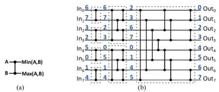
The usual approach for hardware-based sorting is to wire up a network of Compare-and-Swap (CAS) units in a configuration called a Batcher (or bitonic) network (Batcher, 1968). Batcher networks provide low-latency solutions for hardware-based sorting (Farmahini-Farahani et al., 2013; Al-Haj Baddar and Mahafzah, 2014). Each CAS block compares two input values and, if required, swaps the values at the output. Fig. 1(a) shows the schematic symbol of a CAS block. Fig. 1(b) shows the CAS network for an 8-input bitonic sorting network, made up of 24 CAS blocks. Batcher sorting networks are fundamentally different from software algorithms for sorting (such as the quicksort, merge sort, and the bubble sort), since the order of comparisons is fixed in advance. That is, in contrast to software algorithms, the order is data-dependent (Najafi et al., 2018). The implementation cost of a batcher network is a direct function of the number of CAS blocks and the cost of each block. A CAS block is conventionally designed based on the weighted binary radix representation of data. The CAS design consists of an -bit comparator and two -bit multiplexers, where is the data-width of the input data111We note that later on, we take the precision of binary to unary conversion (for unary sorting solution) to be also equal to , the data-width.. Fig. 2(a) shows the conventional design of a CAS unit. In the conventional binary design, increasing the data-width increases the complexity of the design.
(a) … (b)
… (b)
All these prior sorting designs were developed based on the Von-Neumann architecture, separating the memory unit where the data is stored and the processing unit. where the data is processed (i.e., sorted). A significant portion of the total processing time and the total energy consumption is wasted on 1) reading the data from memory, 2) transferring the data between memory and processing unit, and 3) writing the result back into the memory (Balasubramonian et al., 2014) (Keckler et al., 2011) (Ruan et al., 2019) (Koo et al., 2017) (Tseng et al., 2015). In-Memory Computation (IMC) or Processing in Memory (PIM) is an emerging computational approach that offers the ability to both store and process data within memory cells (Zidan et al., 2018; Taherinejad et al., 2015; Radakovits and TaheriNejad, 2019; Hamdioui et al., 2017; Xie et al., 2017; Taherinejad et al., 2016; Gupta et al., 2020; Alam et al., 2021). This technique eliminates the high overhead of transferring data between memory and processing unit, improving the performance and reducing the energy consumption by processing data in memory. Memristive storage is a Non-Volatile Memory (NVM) with high storage density and IMC capability. This emerging technology is one of the most promising candidates for the next generation of storage systems. The IMC capability of NVM devices allows accelerating sorting by avoiding the overheads of transferring the data between memory and processing unit. New sorting approaches based on NVM technology are on the table to increase the efficiency of the hardware-based sorters. Some previous studies worked on optimizing sorting algorithms for NVM and presented NVM-friendly sorting algorithms (Bey Ahmed Khernache et al., 2018) (Chu et al., 2021). Prasad et al. (Prasad et al., 2021) proposed RIME which provides an API library for sorting algorithms using a bit-level search operation within the memory. They use some additional CMOS circuitry including a sensing circuit to compute the minimum and maximum values by performing XOR operation on the memory peripheral circuits. Some previous studies focused on near storage/memory computing techniques for providing efficient sorting algorithms. Li et al. (Li et al., 2020) proposed IMC-Sort, an in-memory parallel sorting architecture using the hybrid memory cube. Their architecture incorporates a custom parallel sorting unit to accelerate the sort workloads in DRAM based on 3D stacking technology. Pugsey et. al. (Pugsley et al., 2015) suggested 3D-stacked near-data processing for sorting data in DRAM. Processing units and memory are integrated with 3D stacking technology using through-silicon vias. Salamat et al. (Salamat et al., 2021) proposed a near-storage accelerator for databases sort based on the bitonic sort. Their accelerator utilizes an NVMe flash drive with an onboard FPGA chip. The authors in (Qiao et al., 2021) propose FANS; an FPGA accelerated near-storage sorting system. Their system is able to sort hundreds of gigabytes of data on a single Samsung SmartSSD. The authors in (Samardzic et al., 2020) introduced Bonsai, an adaptive FPGA-based near-memory sorting solution. Their design considers the off-chip memory bandwidth and on-chip resources to optimize sorting time. Casper and Olukotun (Pugsley et al., 2015) presented three hardware accelerator designs to perform near-memory database operations including sort. Evaluation results by implementing their designs on FPGA showed close to ideal utilization of available memory bandwidth. These prior works sort the data near-memory or in-memory within peripheral circuitry. None of them perform sorting in memory within the memory array. For a detailed classification of different near- and in-memory computing methods, the readers are referred to (Nguyen et al., 2020).
In this paper, we take advantage of IMC to implement sorting units on memristive memory arrays. To the best of our knowledge, this work introduces the first in-array architectures for high-performance and energy-efficient sorting of data completely in memory (CIM-A using the (Nguyen et al., 2020) terminology). Our work is different from the aforementioned prior works in the sense that all computation results are produced within the memory array. We then go further to show how we can benefit from the concept of Unary Computing (Poppelbaum et al., 1987; Najafi et al., 2018) to improve the sorting hardware further for particular applications. We propose two different architectures. The first architecture, ”Binary Sorting,” is based on the conventional weighted binary representation and is applicable to conventional systems that store the data in memory in the binary format. The second architecture, ”Unary Sorting,” is based on the non-weighted unary representation. For each of these designs, we first discuss the basic operation of sorting two -bit data (i.e., a CAS block). We then elaborate on the design of complete sorting networks, which are made up of the proposed in-memory CAS units. We showcase the role and importance of the achieved gains in the context of a median filter used in image processing applications. Our experiments demonstrate a reduction of 14 and 634 in energy and latency for the proposed binary, and 5.6 and 152 in energy and latency for the proposed unary approach compared to those of the off-memory binary and unary designs when implementing a 33 Median filtering system.
The rest of this paper is structured as follows. Section 2 provides a brief overview of memristive IMC and the unary processing technique used in this work. Section 3 and Section 4 present the proposed in-memory Binary and Unary Sorting designs. Section 5 compares the performance of the proposed designs with the conventional off-memory CMOS-based designs and applies the proposed architectures to an important application of sorting, i.e., median filtering. Finally, conclusions are drawn in Section 7.
2. Background
2.1. Memristive IMC
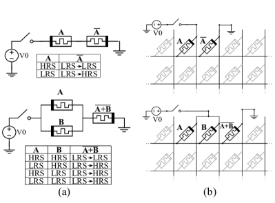
One of the promising technologies for IMC is memristive technology. Among various memristive-based IMC methods, stateful logic such as Material Implication (IMPLY) (Borghetti et al., 2010), Memristor-Aided Logic (MAGIC) (Kvatinsky et al., 2014), FELIX (Gupta et al., 2018), and Single-cycle In-Memristor XOR (SIXOR) (TaheriNejad, 2021) are of the most efficient solutions. In stateful logic, the input and output are both presented as the state of input and output memristors. Hence, no access to the world outside the array (e.g., read or write) is necessary for stateful logic operations. In this work, we use MAGIC NOR operation, which can be used to implement any Boolean logic. MAGIC considers two states of memristors: LRS as logical ‘1’ and HRS as logical ‘0’. Fig. 3(a) shows how NOR and NOT logical operations can be implemented in MAGIC (Kvatinsky et al., 2014), where the memristors connected to the ground are output memristors (Kvatinsky et al., 2014). Before starting the execution of an operation, the output memristors are first initialized to LRS. By applying a specific voltage () to the negative terminal of the input memristors, the output memristors may experience a state change from LRS to HRS, depending on the states of the inputs (Kvatinsky et al., 2014). The truth tables embedded in Fig. 3(a) show all possible cases of the input memristors’ states and switching of the output memristors. Fig. 3(b) shows how MAGIC NOT and NOR can be realized in a crossbar memory. These operations can be natively executed within memory with a high degree of parallelism. Thus, parallel architectures such as sorting networks can benefit greatly from such IMC logic operations.
2.2. In memory Comparator
Comparison is an essential operation in implementing sorting functions. Comparing memory content has been always challenging in computing systems. Content-addressable memory (CAM) (Pagiamtzis and Sheikholeslami, 2006) uses a dedicated equality comparator circuit to return the location of the matching data. CAMs help searching architectures and can be applied to packet forwarding in network routers. Authors in (Prasad et al., 2021) propose a method for finding the minimum and maximum values within a set of numbers in memory. They employ bitwise column search to design a bit-serial algorithm for finding the minimum and maximum value. The sorting mechanisms proposed in (Li et al., 2020) and (Pugsley et al., 2015) are based on a bitonic sorting network and include some comparison units. The comparison units in these works are implemented at the logic layer, which is integrated with 3D stacking DRAM memory banks using through-silicon vias technology. The authors in (Aga et al., 2017) and (Jeloka et al., 2016) further propose two in-memory equality comparators for SRAM memories.
Authors in (Cheng et al., 2020) developed a multivalued 1T1R memristor method for in-memory computing. They exploit the multivalued resistance for performing a 1-bit in-memory comparison and then expand the design to a 4-bit magnitude comparator. Angizi et al propose an in-memory magnitude comparator in (Angizi et al., 2018). Their design uses in-memory XOR operations to perform a bit-wise comparison between corresponding bits of two data beginning from the most significant bit towards the least significant bit. However, the comparison process involves reading the output of the XOR operations and the data from memory by the control unit. Therefore, its latency (i.e., number of processing cycles) is non-deterministic and depends on the data being compared. In Section 3.1, we propose an in-memory magnitude comparator with deterministic latency and no memory read operations (a stateful comparator). Our in-memory comparator does not also need multivalued memristors.
2.3. Unary Sorting
Unary (or burst) processing (Poppelbaum et al., 1987; Poppelbaum, 1978) is an alternative computing paradigm to conventional binary offering simple and noise-tolerant solutions for complex arithmetic functions (Smith, 2018; Jalilvand et al., 2020; Mohajer et al., 2018; Najafi et al., 2018; Faraji and Bazargan, 2020; Madhavan et al., 2014; Tzimpragos et al., 2020; Najafi et al., 2020; Wu et al., 2020). The paradigm borrows the concept of averaging from stochastic computing (Gaines, 1969; Alaghi et al., 2018), but is deterministic and accurate. In unary processing, unlike weighted binary radix, all digits are weighted equally. Numbers are encoded uniformly by a sequence of one value (e.g., 1) followed by a sequence of the other value (e.g., 0) in a stream of 1’s and 0’s– called a unary bit-stream. The value of a unary bit-stream is determined by the frequency of the appearance of 1’s in the bit-stream. For example, 11000000 is a unary bit-stream representing 2/8 or 1/4.
Unary computing was first used in (Najafi et al., 2018; Najafi et al., 2017) for the simple and low-cost implementation of sorting network circuits. Zhang et al. (Zhang et al., 2020) developed an SC-based neural network accelerator by employing a bit-stream-based bitonic sorting network for simultaneously implementing the accumulation and activation functions. With unary bit-streams and also when using correlated stochastic bit-streams (Alaghi and Hayes, 2013), minimum and maximum functions (the main operations in a CAS block) can be implemented using simple standard AND and OR gates. In a serial manner, one AND and one OR gate implements a CAS block by processing one bit of the two bit-streams at each cycle. Hence, a total of processing cycles is needed to process two -bit bit-streams (equivalent to two -bit binary data since we chose the precision of binary to unary conversion to be equal to the data-width, that is, equal to ). More than 90% saving in the hardware cost is reported for a 256-input serial unary sorting circuit at the cost of processing time (Najafi et al., 2018). Alternatively, the bit-streams can be processed in one cycle by replicating the logic gates and performing the logical operations in parallel. Fig 2(b) shows the parallel unary design of a CAS block. pairs of AND and OR gates sort two -bit bit-streams.
3. Proposed In-Memory Binary Sorting
In this section, we present our proposed method for in-memory sorting of binary radix data. First, we discuss the implementation of a basic sorting unit and then generalize the architecture to complete sort systems.
(a)  (b)
(b) 
(a) (b)
(a) (b)

3.1. Basic Binary Sorting Unit
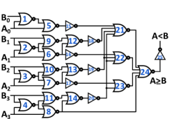
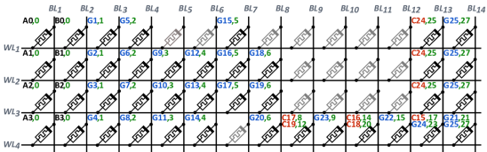
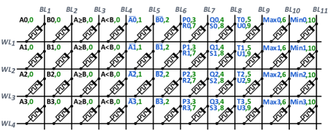
A basic binary sorting unit (CAS unit) requires one comparator and two multiplexers. Implementing an -bit comparator by using basic logic gates requires () NOR and () NOT logic gates. Figs. 4(a) and 5(a) show the generic logic and the NOR-based logic design of a 4-bit binary comparator. Fig. 5(b) shows our proposed in-memory implementation using MAGIC. As shown, implementing this comparator using MAGIC NOR and NOT operations requires a crossbar with memory cells. The input data (i.e., A and B) in binary format is stored in two different columns (BL1 and BL2), each column containing memristors, where is the size of the data being compared (in this example, ). The computation includes NOR, NOT, and copy operations. Each memristor in Fig. 5(b) shows participation in a logical gate (operation) in Fig. 5(a). s on the other hand, show the copy operation , in which the state of memristor is duplicated. The index marks the cycle number in which an operation is performed. In some cases, a memristor participates in two operations. For example, the memristor at the right-bottom end of Fig. 5(b) (WL4, BL14) is once used at cycle 21 in gate (operation) 21 and once at cycle 27 in gate (operation) 25.
To execute these operations, in each clock cycle, the memristor controller applies the proper voltage to crossbar columns and rows to execute some NOR or NOT operations concurrently. All memristors with the same cycle number produce their output value at the same time. When possible, we reuse memristors to avoid increasing area, i.e., the number of used memristors. The memristors that are being re-used as an output must be initialized to LRS in an additional clock cycle before reusing. The comparison result (i.e., the output of gate 24) is ready at cycle 23 on (WL4, BL13). At this time, some copies from the comparison result and its complement must be made. These will be used as the select inputs of the maximum and minimum multiplexers shown in Fig. 4(b) and Fig. 6. To this end, first, we make three copies of the output of gate 24 on three memristors in the same column (BL13) and then invert these memristors on another column (BL14) to make the required complements. This leads to a total processing time of 27 cycles plus one initialization cycle.
After the comparison process, we need values of only four columns (BL1 and BL2 for the two input data, and BL13 and BL14 for the two comparison results) to implement the multiplexer part of the sorting unit. Hence, we could reuse the rest of the memristors. Fig. 4(b) and Fig. 6 show the generic logic and the NOR-based logic circuit for a multi-bit 2-to-1 multiplexer. Fig. 6 shows our MAGIC-based in-memory design for the two 4-bit multiplexers the sorting circuit requires to select the maximum and minimum data. In implementing the multiplexers, we re-use the memory cells of the comparison step. To this end, we initialize the columns used in the comparison step (BL3 to BL12) to LRS in one clock cycle. The input data is inverted in two clock cycles, cycles 1 and 2 (on BL4 and BL5) shown in Fig. 6. The first multiplexer produces the maximum value on BL10 in cycles 3 to 6. The minimum value is produced on BL11 by the second multiplexer through cycles 7 to 10. Since three columns used by the first multiplexer (i.e., P, Q, T) are being re-used by the second multiplexer, an additional cycle is considered for the initialization of these columns before execution of the second multiplex operation. The execution of the multiplexers, therefore, takes two initialization and 10 operation cycles. Hence, execution of the proposed in-memory basic binary sorting takes a total of 39 processing cycles plus one initialization cycle.
We extend the proposed design from sorting of 4-bit data to higher data-widths, namely 8-, 16-, 32-, and in general -bit data. We verified the correct functionality of the proposed design by high-level simulation and measured the energy and delay numbers by circuit-level simulation using Cadence Virtuoso. Table 1 reports the required resources, the number of cycles, and energy consumption. Further details on circuit-level simulations and the parameter values used in estimating the energy numbers will be discussed in Section 5.1. We see that the area, the latency, and the energy consumption of the proposed basic binary sorting design increase linearly by increasing the data-width.
| Data-Width | Required | # of Initialized | # of Reused | # of Logical | # of Copies | Reused init | Total # of | Energy |
| Dimension | Memristors | Memristors | Operation Cycles | [Copy Cycles] | Cycles | Cycles | () | |
| 4 | 414 | 40 | 44 | 21 | 6 (12) | 6 | 39 | 199.4 |
| 8 | 822 | 88 | 88 | 25 | 14 (28) | 10 | 63 | 417 |
| 16 | 1638 | 184 | 176 | 33 | 30 (60) | 18 | 111 | 845 |
| 32 | 3270 | 376 | 352 | 49 | 62 (124) | 34 | 207 | 1728 |
| (8+2-2) | 18+(-1) | 2-2 [2(2-2)] | 6 | - |
3.2. Complete Binary Sort System
A complete sort network is made of basic sorting units (i.e., CAS blocks). In bitonic sorting, the network recursively merges two sets of size to make a sorted set of size (Gedik et al., 2007). Fig. 1 shows the CAS network for an 8-input bitonic sorting. As it can be seen, the network is made of 24 CAS units. In general, an -input bitonic sorting network requires
| (1) |
CAS units. These CAS units can be split into
| (2) |
steps (also known as stages), each with /2 CAS units that can operate in parallel (Farmahini-Farahani et al., 2013).
Bitonic Sorting Networks (DW = Data-Width, BL = Bit-Stream Length)
| Network Size | Binary Sorting DW = 4 | DW = 8 | DW = 16 | DW = 32 | ||||||||
| Cycles | Size | Energy | Cycles | Size | Energy | Cycles | Size | Energy | Cycles | Size | Energy | |
| 4 | 128 | 428 | 1.2 | 200 | 844 | 2.5 | 344 | 1676 | 5.1 | 632 | 32140 | 10 |
| 8 | 280 | 456 | 4.7 | 424 | 888 | 10 | 712 | 16152 | 20 | 1288 | 32280 | 41 |
| 16 | 544 | 4112 | 15 | 784 | 8176 | 33 | 1264 | 16304 | 68 | 2224 | 32560 | 138 |
| 32 | 1048 | 4224 | 47 | 1408 | 8352 | 100 | 2128 | 16608 | 205 | 3568 | 321120 | 415 |
| Network Size | Unary Sorting BL = 16 | BL = 64 (DW = 6) | BL = 256 (DW = 8) | BL = 1024 (DW = 10) | ||||||||
| Cycles | Size | Energy | Cycles | Size | Energy | Cycles | Size | Energy | Cycles | Size | Energy | |
| 4 | 26 | 1610 | 1.37 | 26 | 6410 | 5.4 | 26 | 25610 | 21.88 | 26 | 102410 | 87 |
| 8 | 76 | 1620 | 5.4 | 76 | 6420 | 21 | 76 | 25620 | 87 | 76 | 102420 | 350 |
| 16 | 194 | 1640 | 18 | 194 | 6440 | 72 | 194 | 25640 | 291 | 194 | 102440 | 1168 |
| 32 | 538 | 1680 | 54 | 538 | 6480 | 218 | 538 | 25680 | 875 | 538 | 102480 | 3503 |
| 64 | 1406 | 16160 | 153 | 1406 | 64160 | 613 | 1406 | 256160 | 2452 | 1406 | 1024160 | 9809 |
| 128 | 3624 | 16320 | 408 | 3624 | 64320 | 1635 | 3624 | 256320 | 6540 | 3624 | 1024320 | 26159 |
| 256 | 9176 | 16640 | 1051 | 9176 | 64640 | 4204 | 9176 | 256640 | 16817 | 9176 | 1024640 | 67268 |
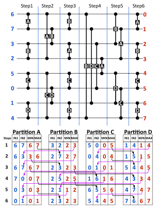
Gupta et al (Gupta et al., 2018) propose a memory partitioning method to improve the in-memory parallelism. In a similar fashion, we split the memory into multiple partitions to enable parallel execution of different CAS operations in each bitonic CAS stage. Fig. 7 shows how we implement an 8-input bitonic sorting network in memory. The memory is split into four partitions, namely partitions A, B, C, and D (each marked on a black vertical line in the bitonic network representation). The number of partitions is decided based on the number of CAS units that can run in parallel (i.e., .). Each partition includes two out of the eight unsorted input data. The sorting process is split into six steps equal to the number of CAS groups (stages). In the first step, the two inputs in each partition are sorted using the basic sorting operation proposed in Section II-A. In the second step, each maximum number (i.e., the larger number between the two in the partition) found by the sorting operations of the first step is copied to another partition where it is needed. The bitonic network determines the destination partition. For instance, the maximum found by executing the sorting operation in partition A (i.e., the input with a value of 7 in the example of Fig. 7) will be copied into partition B to be compared with the minimum number between the two initial data in partition B of the first step. Similarly, in each one of the next steps (i.e., steps 3 to 6), one output data from each partition is copied to another partition, and a sorting operation is executed.
In each step, the sortings in different partitions are executed in parallel. After six steps and the execution of a total of 24 (=) basic sorting operations, the sorted data is ready in the memory. Each basic sorting operation is implemented based on the in-memory basic binary sorting proposed in Section 3.1. Table 2 shows the total number of processing cycles, the required size of crossbar memory, and the energy consumption of different sizes of in-memory bitonic networks. The total number of processing cycles, , is calculated using
| (3) |
where is the number of processing cycles necessary to execute a basic sorting operation, is the number of copy operations, and the number of sorting steps. The required size of crossbar memory () is found by
| (4) |
where is the size of the crossbar memory required for one basic sorting unit222We remember that is the data-width and is the network size or the total number of items to be sorted..
4. Proposed In-Memory Unary Sorting
In this section, we propose a novel method for sorting unary data in memory to avoid the overheads of off-memory processing in the unary systems. We first discuss the basic operation of sorting two unary bit-streams in memory and then elaborate on the design of a complete unary sorting network.
4.1. Basic Unary Sorting Unit
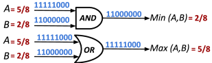
The maximum and minimum functions are the essential operations in a basic sorting unit. Performing bit-wise logical AND on two unary bit-streams with the same length gives the minimum of the two bit-stream. Bit-wise logical OR, on the other hand, gives the maximum of the two unary bit-streams with the same length. Fig. 8 shows an example of the maximum and the minimum operation on two unary bit-streams. The example presents these operations in a serial manner by processing one bit of the input bit-streams at each cycle. While the serial approach is extremely simple to implement with only one pair of AND and OR gates, it incurs a long latency proportional to the length of the bit-streams. In this work, we choose the precision of binary to unary conversion equal to the data-width, . This means an -bit data in the binary domain corresponds to a -bit bit-stream in the unary domain. This implies a latency of cycles with a serial unit. Parallel sorting of two -bit precision data represented using two -bit bit-streams requires performing logical AND operations (to produce the minimum bit-stream), and logical OR operations (to produce the maximum bit-stream) in parallel as shown in Fig 2(b). The suitability of the memristive crossbar for running parallel logical operations in memory makes it a perfect place for low-latency parallel sorting of unary bit-streams.
(a) …….. (b)
|
|
|
|
|
|
|
|
|
||||||||||||||||||
| 64 | 32 | 32 | 48 | 1 | 5 | 227 | ||||||||||||||||||||
| 256 | 128 | 128 | 192 | 1 | 5 | 910 | ||||||||||||||||||||
| 1024 | 512 | 512 | 768 | 1 | 5 | 3640 | ||||||||||||||||||||
| 4096 | 2048 | 2048 | 3072 | 1 | 5 | 14558 |
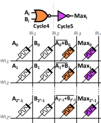
Fig. 9 shows our proposed design for MAGIC-based in-memory execution of minimum and maximum operations on two unary bit-streams. As shown in Fig. 9, implementing this sorting unit using MAGIC NOR and NOT operations requires a memristor crossbar proportional to the length of the bit-streams. The unsorted unary data (i.e., A and B bit-streams) are stored in two different columns (BL1 and BL2). Both inputs have the same length of . As shown in Fig. 9, the AND operation (minimum function) is realized by first inverting the bit-streams through MAGIC NOT and then performing bit-wise MAGIC NOR on the inverted bit-streams. This effectively implements the AND operation as . The first and the second bit-stream are inverted on BL3 and BL4 in the first and the second cycle, respectively. The NOR operation is executed in the third cycle on BL5. As shown in Fig. 9, the OR operation (maximum function) is achieved by first performing MAGIC NOR on the input bit-streams and then MAGIC NOT on the outputs of the NOR operations. Hence, the execution of the OR operation takes two cycles.
The columns that we use during the execution of the AND operation to store the inverted version of the bit-streams (e.g., the third and fourth columns in Fig. 9) are re-used in the execution of the OR operation to avoid using additional memristors. In contrast to the proposed in-memory binary sorting of Section 3.1, which has a variable latency dependent on the width of the input data, the processing latency of the proposed unary sorting is fixed at five cycles and does not change with the data-width. Table 3 shows the required resources, number of cycles, and energy consumption of the proposed basic sorting unit for different bit-stream lengths.
The number of memristors is directly proportional to the length of the bit-streams. In a fully parallel design approach, the size of the memory, particularly the number of rows, defines an upper-limit on the maximum data-width for the to-be-sorted unary data. In such a system, bit-streams with a length longer than the number of rows can be supported by splitting each bit-stream into multiple shorter sub-bit-streams, storing each sub-bit-stream in a different column, and executing the CAS operations in parallel. The sub-results will be finally merged to produce the complete minimum and maximum bit-streams. This design approach sorts the data with reduced latency as the primary objective. A different approach for sorting long bit-streams is to perform CAS operations on the sub-bit-streams in a serial manner by re-using the CAS unit(s). The above approach reduces the area (number of used memristors) at the cost of additional latency. In this case, after sorting each pair of sub-bit-streams, the result is saved, and a new pair of sub-bit-stream is loaded for sorting. Assuming that each input bit-stream is split into sub-bit-streams, the number of processing cycles to sort each pair of input data increases by a factor of . Some additional processing cycles are also needed for saving each sub-output and copying each pair of sub-input. Combining the parallel and the serial approach is also possible for further trade-offs between area and delay. These approaches increase the range of supported data-widths but incur a more complicated implementation and partition management.
4.2. Complete Unary Sort System
Implementing a bitonic sorting network in the unary domain follows the same approach as presented in Section 3.2 for binary implementation of sorting networks. The number of sorting steps and the required number of basic sorting operations are exactly the same as those of the binary sorting network design. The essential difference, however, is that in the unary sorting system, the data is in the unary format. Therefore, the basic 2-input sorting operation should be implemented based on the unary sorting unit proposed in Section 4.1. Table 2 shows the number of processing cycles and the required size of memory for implementing unary bitonic networks of different sizes. We report the latency, area, and energy of these networks as well.
5. Comparison and Application
5.1. Circuit-Level Simulations
We implemented a 1616 crossbar and necessary control signals in Cadence Virtuoso for circuit-level evaluation of the proposed designs. For memristor simulations, we used the Voltage Controlled ThrEshold Adaptive Memristor (VTEAM) model (Kvatinsky et al., 2015). The Parameters used for the VTEAM model can be seen in Table 4. We evaluated the designs in an analog mixed-signal environment by using the Spectre simulation platform with 0.1 transient step. For MAGIC operations, we applied = with 1 pulse-width to initialize the output memristors to LRS. For the simplicity of controller design, we consider the clock cycle period of 1.25 and pulse-width of 1 for all operations. voltage for NOT, 2-input NOR, 3-input NOR, and 4-input NOR is , , , and , respectively. We perform the copy operations by using two consecutive NOT operations.
To estimate the total energy of in-memory computations, we first find the energy consumption of each operation. The energy number measured for each operation depends on the states of input memristors (i.e., LRS, HRS). We consider all possible cases when measuring the energy of each operation. For example, the 3-input NOR has eight possible combinations of input states. We consider the average energy of these eight cases as the energy of 3-input NOR. The average measured energy of different operations is reported in Table 5. Note that higher energy consumption for NOT operation compared to 2-input NOR is due to using a higher voltage for NOT. The reported energy for the proposed in-memory sorting designs is the sum of the energy consumed by all operations.
| Parameter | Value | Parameter | Value |
|---|---|---|---|
| 1 k | 3 | ||
| 300 k | -216.2 m/sec | ||
| -1.5 V | 0.091 m/sec | ||
| 300 mV | 4 | ||
| 0 nm | 4 |
| Operation | Average Energy |
|---|---|
| memristor initialization | 2350 |
| memristor copy | 40.08 |
| NOT | 20.04 |
| 2-input NOR | 9.01 |
| 3-input NOR | 37.24 |
| 4-input NOR | 54.51 |
5.2. Comparison of In- and Off-Memory
We compare the latency and energy consumption of the proposed in-memory binary and unary sorting designs with the conventional off-memory CMOS-based designs for the case of implementing bitonic networks with a data-width of eight. For a fair comparison, we assume that the to-be-sorted data are already stored in memristive memory when the sorting process begins and hence do not consider the delay for initial storage. We do not consider this latency because it is the same for both cases of the proposed in-memory and the off-memory counterparts. For the case of off-memory binary designs, we assume 8-bit precision data are read from and written to a memristive memory. For the case of off-memory unary design, we evaluate two approaches: 1) unary data (i.e., 256-bit bit-streams) are read from and written to memory, and 2) 8-bit binary data are read from and written to memory. For the second approach, the conversion overhead (i.e., binary to/from unary bit-stream) is also considered. This conversion is performed off-memory using combinational CMOS logic (Najafi et al., 2018). The conventional CMOS-based off-memory sorting systems read the raw data from memory, sort the data with CMOS logic, and write the sorted data into memory. These read and write operations take the largest portion of the latency and energy consumption. We use the per-bit read and write latency and per-bit energy consumption reported in (Xu et al., 2011) to calculate the total latency and energy of reading from and writing into the memristive memory. For the proposed in-memory designs, the entire processing step is performed in memory, and so there is no read and write operations from and to the memory. For the off-memory cases, we do not incorporate the transferring overhead between the memory and the processing unit as it depends on the interconnects used. We implemented the off-memory processing units using Verilog HDL and synthesized them using the Synopsys Design Compiler v2018.06-SP2 with the 45nm NCSU-FreePDK gate library.
Table 6 shows the summary of performance results. As reported, the proposed in-memory designs provide a significant latency and energy reduction, compared to the conventional off-memory designs. That is, on average 14 and 37, respectively, for the binary sorting. For the unary design, the average latency and energy reductions are 1200 and 138, respectively. For the unary systems with the data stored in memory in a binary format, the proposed in-memory design can reduce the latency and energy by a factor of up to 65 and 9.7, respectively. For a realistic and more accurate energy consumption comparison, however, the overhead of transferring data on the interconnect between the memory and the processing unit must be added for the off-memory cases. We note that these numbers are highly dependent on the architecture of the overall system and the interconnects used. Therefore, different system architectures may substantially change these numbers; however, they do not change the fact that our proposed method is more advantageous. In fact, they only change the extent of this improvement (and further increase it) since no data transfer happens in the in-memory sorting solution. Hence, by eliminating them, we present the minimum improvement obtained by our method and leave the further improvement to the final implementation details of designers.
| Network Size | 8 | 16 | 32 | 64 | 128 | 256 | ||||||
| Design Method | E | L | E | L | E | L | E | L | E | L | E | L |
| Off-Memory Binary Sorting (+ Binary R/W) | 850 | 6.5 | 1701 | 13 | 3403 | 26 | 6806 | 52 | 13613 | 104 | 27227 | 209 |
| Proposed In-Memory Binary Sorting | 10 | 0.55 | 33 | 1.02 | 100 | 1.8 | 281 | 3.4 | 794 | 6.8 | 1927 | 14 |
| Off-Memory Unary Sorting (+ Binary R/W) | 851 | 6.5 | 1703 | 13 | 3406 | 26 | 6811 | 52 | 13622 | 104 | 27244 | 209 |
| Off-Memory Unary Sorting (+ Unary R/W) | 27226 | 210 | 54452 | 419 | 108904 | 839 | 217809 | 1679 | 435618 | 3358 | 871236 | 6717 |
| Proposed In-Memory Unary Sorting | 87 | 0.10 | 291 | 0.25 | 875 | 0.7 | 2452 | 1.8 | 6,540 | 4.7 | 16,817 | 12 |
5.3. Application to Median Filtering
Median filtering has been widely used in different applications, from image and video to speech and signal processing. In these applications, digital data is often affected by noise. A median filter —which replaces each input data with the median of all the data in a local neighborhood (e.g., a 33 local window)— is used to filter out impulse noises and smoothen the data (Nikahd et al., 2016). A variety of methods for the implementation of Median filters have been proposed. Sorting network-based architectures made of CAS blocks are one of the most common approaches (Najafi et al., 2018). The incoming data is sorted as it passes the network. The middle element of the sorted data is the median. We developed in-memory architectures for a and a median filtering based on our proposed in-memory binary and unary sorting designs.
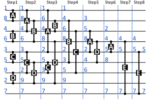
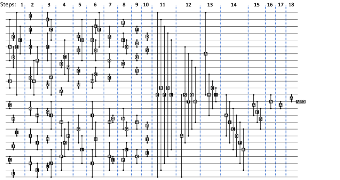
Fig. 10 and Fig. 11 depict a high-level flow of memory partitioning for our in-memory and Median filter design. Similar to our approach in implementing the complete sort system, the memory is split into multiple partitions. For the design, partitions are A, B, C, D, and E (five partitions), and for the design, they are A to T (20 partitions). Each sorting unit sorts the data in one particular partition. Some partitions are initialized with the input data in the first step and the others are initialized and used in the following steps. The process is split into eight steps for the , and to 18 steps for the design, each step executing some basic sorting operations in parallel. After each step, to prepare data for the next step, some data must be transferred between partitions similar to what we did in sorting. These data transfers are done by using copy operations. Compared to a complete sorting network, fewer sorting units are required as only the median value is targeted.
We evaluated the implementation of these basic sorting operations using both the proposed binary and unary bit-stream-based in-memory architectures. Table 7 reports the latency, the number of required memristors, and the energy consumption of the developed designs for (i) a single Median filter and a single Median filter and (ii) a and a Median filter image processing system that process images of size. The corresponding latency and energy consumption of the off-memory CMOS-based binary and unary designs are also reported in Table 7. As it can be seen, the proposed in-memory binary and unary designs reduce the energy by a factor of 14 and 5.6, respectively, for the -based image processing system, and 3.1 and 12 for the -based image processing system, compared to their corresponding off-memory designs. The latency of the binary and unary design is also reduced by a factor of 634 and 152 with the window, and by a factor of 110 and 19.2 with the window, for the image processing system.
Note that we did not incorporate the overhead latency and the energy of transferring data on the bus or other interconnects for the off-memory cases, which is a large portion of energy of consumption in transferring data between memory and processing unit (Keckler et al., 2011). By considering this overhead, our approach would have a significantly larger advantage over others in a complete system.
| Median Filter 3 3 | |||||||
| Design | E ( J) | L ( s) | Design | E ( J) | L ( s) | ||
| Proposed Binary | 544 | 8 110 | 0.0085 | 0.68 | Off-Memory Binary | 0.121 | 0.94 |
| Proposed Unary | 72 | 256 25 | 0.069 | 0.09 | Off-Memory Unary | 3.882 | 30.17 |
| 64 64 Image Processor | |||||||
| Proposed Binary | 4896 | 208 1980 | 35 | 6.1 | Off-Memory Binary | 490 | 3870 |
| Proposed Unary | 684 | 2048 1425 | 283 | 0.81 | Off-Memory Unary | 1590 | 123578 |
| Median Filter 5 5 | |||||||
| Design | E ( J) | L ( s) | Design | E ( J) | L ( s) | ||
| Proposed Binary | 1416 | 8 440 | 0.049 | 1.77 | Off-Memory Binary | 0.151 | 1.19 |
| Proposed Unary | 259 | 256 100 | 0.401 | 0.324 | Off-Memory Unary | 4841 | 38.02 |
| 64 64 Image Processor | |||||||
| Proposed Binary | 35400 | 328 1760 | 200 | 44.25 | Off-Memory Binary | 620 | 4875 |
| Proposed Unary | 6475 | 2048 2000 | 1643 | 8.09 | Off-Memory Unary | 19829 | 155739 |
6. Discussion
The high latency and energy overhead of reading from and writing to memory, and transferring data between the processing unit and memory, take up a significant amount of resources in sorting data in the conventional systems. IMC is a promising solution to mitigate these overheads. IMC is particularly beneficial for 1) applications with large data or a large number of memory accesses and 2) applications with extensive parallelism that can independently run a large number of operations in parallel. Sorting is one of the applications that has both properties. As we showed, implementing sorting in memory can save significant time and energy by avoiding the overheads of memory access and off-chip data transfer. This is particularly important for the unary systems, where data are stored in memory in the form of long bit-streams. Reading and writing long bit-streams from and to memory make off-memory unary sorting highly inefficient. However, one should note that the size of the memory array puts an upper limit on the size of the sorting network and the data-width. For example, given a (memristive) memory array of , the proposed binary sorting approach supports the complete sorting of 64 8-bit and 128 4-bit input data. For the proposed unary approach, an array of that size (1Mb or 128kB) supports the complete sorting of 256 1024-bit unary bit-streams. For the larger bit-streams or data-width, or larger number of data to be sorted, we would need to partition the data into different arrays. That means a more complex control and partition management mechanism, which reduces the benefits of fully in-array sorting.
Memristive technology is an emerging technology still in evolution, with many competing implementation methods in the process of maturation (TaheriNejad and Radakovits, 2019). Properties such as the delay, power, and energy consumption are heavily dependent on the used technology and change considerably from one to another. In this article, the experimental results are provided by simulation tools using the VTEAM model. Using different memristive technologies and models, LRS and HRS values, as well as programming or reading pulses with different amplitude or width, affect the actual delay and energy numbers reported here. The actual memristive implementation is a showcase of the feasibility and meaningfulness of such an in-memory sorting design. That is, there exists an in-memory implementation (namely using the memristive technology we have used here) to be significantly beneficial. Therefore, we consider the properties and comparison of other ways of implementing our proposed architecture (using CMOS IMC, other memristor technologies, or other emerging memory technologies) as an exciting future work but outside the current article’s scope. Nonetheless, we would like to point out that we have provided the number of memristors (memory cells) and the number of operation cycles that are technology-independent. Therefore, others can independently evaluate and compare their own implementations with ours in a technology-agnostic fashion and using the number of memory cells and the number of cycles their implementation needs (regardless of the LRS and HRS values or pulse amplitude and width).
7. Conclusion
Thus far, sorting solutions were based on the conventional approach of processing off-memory, incurring a high overhead of reading/writing from/to memory and transferring between the memory and the processing unit. In this paper, for the first time -to the best of our knowledge- we developed two methods for in-array sorting of data: a binary and a unary sorting design. We compared the area, latency, and energy consumption of the basic and the complete sorting systems for different data-widths and network sizes. The latency and energy are significantly reduced compared to prior off-memory CMOS-based sorting designs. Further, we developed in-memory binary and unary designs for an important sorting application, median filtering. In future works, we plan to extend the proposed architectures to other applications of sorting, for instance, efficient in-memory implementation of weighted and adaptive median filters. We will also explore applications of in-memory sorting in communications and coding domains.
References
- (1)
- Aga et al. (2017) Shaizeen Aga, Supreet Jeloka, Arun Subramaniyan, Satish Narayanasamy, David Blaauw, and Reetuparna Das. 2017. Compute Caches. In 2017 IEEE International Symposium on High Performance Computer Architecture (HPCA). 481–492. https://doi.org/10.1109/HPCA.2017.21
- Al-Haj Baddar and Mahafzah (2014) Sherenaz W. Al-Haj Baddar and Basel A. Mahafzah. 2014. Bitonic Sort on a Chained-cubic Tree Interconnection Network. JPDC 74, 1 (2014), 1744–1761. https://doi.org/10.1016/j.jpdc.2013.09.008
- Alaghi and Hayes (2013) Armin Alaghi and John P. Hayes. 2013. Exploiting correlation in stochastic circuit design. In 2013 IEEE 31st International Conference on Computer Design (ICCD). 39–46. https://doi.org/10.1109/ICCD.2013.6657023
- Alaghi et al. (2018) Armin Alaghi, Weikang Qian, and John P. Hayes. 2018. The Promise and Challenge of Stochastic Computing. IEEE Transactions on Computer-Aided Design of Integrated Circuits and Systems 37, 8 (2018), 1515–1531. https://doi.org/10.1109/TCAD.2017.2778107
- Alam et al. (2021) Mohsen Riahi Alam, M. Hassan Najafi, and Nima Taheri Nejad. 2021. Exact Stochastic Computing Multiplication in Memristive Memory. IEEE Design Test (2021), 1–1. https://doi.org/10.1109/MDAT.2021.3051296
- Angizi et al. (2018) Shaahin Angizi, Zhezhi He, Adnan Siraj Rakin, and Deliang Fan. 2018. CMP-PIM: An Energy-Efficient Comparator-Based Processing-in-Memory Neural Network Accelerator. In Proceedings of the 55th Annual Design Automation Conference (San Francisco, California) (DAC ’18). Association for Computing Machinery, New York, NY, USA, Article 105, 6 pages. https://doi.org/10.1145/3195970.3196009
- Balasubramonian et al. (2014) Rajeev Balasubramonian, Jichuan Chang, Troy Manning, Jaime H. Moreno, Richard Murphy, Ravi Nair, and Steven Swanson. 2014. Near-Data Processing: Insights from a MICRO-46 Workshop. IEEE Micro 34, 4 (2014), 36–42. https://doi.org/10.1109/MM.2014.55
- Batcher (1968) Ken E. Batcher. 1968. Sorting Networks and Their Applications. In Proceedings of the April 30–May 2, 1968, Spring Joint Computer Conference (Atlantic City, New Jersey) (AFIPS ’68 (Spring)). Association for Computing Machinery, New York, NY, USA, 307–314. https://doi.org/10.1145/1468075.1468121
- Bey Ahmed Khernache et al. (2018) Mohammed Bey Ahmed Khernache, Arezki Laga, and Jalil Boukhobza. 2018. MONTRES-NVM: An External Sorting Algorithm for Hybrid Memory. In 2018 IEEE 7th Non-Volatile Memory Systems and Applications Symposium (NVMSA). 49–54. https://doi.org/10.1109/NVMSA.2018.00013
- Borghetti et al. (2010) Julien Borghetti, Gregory S. Snider, Philip J. Kuekes, J. Joshua Yang, Duncan R. Stewart, and Richard Stanley Williams. 2010. ‘Memristive’ switches enable ‘stateful’ logic operations via material implication. Nature 464 (April 2010), 873–876. https://doi.org/10.1038/nature08940
- Brajovic and Kanade (1999) Vladimir Brajovic and Takeo Kanade. 1999. A VLSI sorting image sensor: global massively parallel intensity-to-time processing for low-latency adaptive vision. IEEE Transactions on Robotics and Automation 15, 1 (1999), 67–75. https://doi.org/10.1109/70.744603
- Capannini et al. (2012) Gabriele Capannini, Fabrizio Silvestri, and Ranieri Baraglia. 2012. Sorting on GPUs for large scale datasets: A thorough comparison. Information Processing & Management 48, 5 (2012), 903 – 917. https://doi.org/10.1016/j.ipm.2010.11.010 Large-Scale and Distributed Systems for Information Retrieval.
- Cederman and Tsigas (2010) Daniel Cederman and Philippas Tsigas. 2010. GPU-Quicksort: A Practical Quicksort Algorithm for Graphics Processors. ACM JEA 14, Article 4 (2010), .84 pages. https://doi.org/10.1145/1498698.1564500
- Chakrabarti and Wang (1994) Chaitali Chakrabarti and Li-Yu Wang. 1994. Novel sorting network-based architectures for rank order filters. IEEE TVLSI 2, 4 (Dec 1994), 502–507. https://doi.org/10.1109/92.335027
- Chen and Prasanna (2017) Ren Chen and Viktor K. Prasanna. 2017. Computer Generation of High Throughput and Memory Efficient Sorting Designs on FPGA. IEEE Transactions on Parallel and Distributed Systems 28, 11 (2017), 3100–3113. https://doi.org/10.1109/TPDS.2017.2705128
- Cheng et al. (2020) Long Cheng, Hao-Xuan Zheng, Yi Li, Ting-Chang Chang, Simon M. Sze, and Xiangshui Miao. 2020. In-Memory Digital Comparator Based on a Single Multivalued One-Transistor-One-Resistor Memristor. IEEE Transactions on Electron Devices 67, 3 (2020), 1293–1296. https://doi.org/10.1109/TED.2020.2967401
- Chu et al. (2021) Zhaole Chu, Yongping Luo, Peiquan Jin, and Shouhong Wan. 2021. NVMSorting: Efficient Sorting on Non-Volatile Memory. In The 33rd International Conference on Software Engineering & Knowledge Engineering (SEKE 2021).
- Colavita et al. (1997) Alberto Colavita, Enzo Mumolo, and Gabriele Capello. 1997. A novel sorting algorithm and its application to a gamma-ray telescope asynchronous data acquisition system. Nuclear Inst. and Methods in Physics Research Sec. A 394, 3 (1997), 374 – 380. https://doi.org/10.1016/S0168-9002(97)00567-6
- Faraji and Bazargan (2020) S. Rasoul Faraji and Kia Bazargan. 2020. Hybrid Binary-Unary Hardware Accelerator. IEEE Trans. Comput. 69, 9 (2020), 1308–1319. https://doi.org/10.1109/TC.2020.2971596
- Farmahini-Farahani et al. (2013) Amin Farmahini-Farahani, Henry J. Duwe III, Michael J. Schulte, and Katherine Compton. 2013. Modular Design of High-Throughput, Low-Latency Sorting Units. IEEE Trans. Comput. 62, 7 (2013), 1389–1402. https://doi.org/10.1109/TC.2012.108
- Gaines (1969) Brian R. Gaines. 1969. Stochastic Computing Systems. In Advances in Information Systems Science. Springer US, 37–172. https://doi.org/10.1007/978-1-4899-5841-9_2
- Gedik et al. (2007) Buǧra Gedik, Rajesh R. Bordawekar, and Philip S. Yu. 2007. CellSort: High Performance Sorting on the Cell Processor. In VLDB (Vienna, Austria). 1286–1297.
- Govindaraju et al. (2006) Naga Govindaraju, Jim Gray, Ritesh Kumar, and Dinesh Manocha. 2006. GPUTeraSort: High Performance Graphics Co-processor Sorting for Large Database Management. In SIGMOD (Chicago, IL, USA). 325–336. https://doi.org/10.1145/1142473.1142511
- Graefe (2006) Goetz Graefe. 2006. Implementing Sorting in Database Systems. ACM Comput. Surv. 38, 3, Article 10 (Sept. 2006). https://doi.org/10.1145/1132960.1132964
- Gupta et al. (2018) Saransh Gupta, Mohsen Imani, and Tajana Rosing. 2018. FELIX: Fast and Energy-Efficient Logic in Memory. In 2018 IEEE/ACM International Conference on Computer-Aided Design (ICCAD). 1–7. https://doi.org/10.1145/3240765.3240811
- Gupta et al. (2020) Saransh Gupta, Mohsen Imani, Joonseop Sim, Andrew Huang, Fan Wu, M. Hassan Najafi, and Tajana Rosing. 2020. SCRIMP: A General Stochastic Computing Architecture using ReRAM in-Memory Processing. In 2020 Design, Automation Test in Europe Conference Exhibition (DATE). 1598–1601. https://doi.org/10.23919/DATE48585.2020.9116338
- Hamdioui et al. (2017) Said Hamdioui, Shahar Kvatinsky, Gert Cauwenberghs, Lei Xie, Nimrod Wald, Siddharth Joshi, Hesham Mostafa Elsayed, Henk Corporaal, and Koen Bertels. 2017. Memristor for Computing: Myth or Reality? (DATE ’17).
- Jalilvand et al. (2020) Amir Hossein Jalilvand, M. Hassan Najafi, and Mahdi Fazeli. 2020. Fuzzy-logic using Unary Bit-Stream Processing. In 2020 IEEE International Symposium on Circuits and Systems (ISCAS). 1–5.
- Jeloka et al. (2016) Supreet Jeloka, Naveen Bharathwaj Akesh, Dennis Sylvester, and David Blaauw. 2016. A 28 nm Configurable Memory (TCAM/BCAM/SRAM) Using Push-Rule 6T Bit Cell Enabling Logic-in-Memory. IEEE Journal of Solid-State Circuits 51, 4 (2016), 1009–1021. https://doi.org/10.1109/JSSC.2016.2515510
- Keckler et al. (2011) Stephen W. Keckler, William J. Dally, Brucek Khailany, Michael Garland, and David Glasco. 2011. GPUs and the Future of Parallel Computing. IEEE Micro 31, 5 (2011), 7–17. https://doi.org/10.1109/MM.2011.89
- Koch and Torresen (2011) Dirk Koch and Jim Torresen. 2011. FPGASort: A High Performance Sorting Architecture Exploiting Run-time Reconfiguration on FPGAs for Large Problem Sorting. In FPGA. https://doi.org/10.1145/1950413.1950427
- Koo et al. (2017) Gunjae Koo, Kiran Kumar Matam, Te I., H.V. Krishna Giri Narra, Jing Li, Hung-Wei Tseng, Steven Swanson, and Murali Annavaram. 2017. Summarizer: Trading Communication with Computing Near Storage. In 2017 50th Annual IEEE/ACM International Symposium on Microarchitecture (MICRO). 219–231.
- Kvatinsky et al. (2014) Shahar Kvatinsky, Dmitry Belousov, Slavik Liman, Guy Satat, Nimrod Wald, Eby G. Friedman, Avinoam Kolodny, and Uri C. Weiser. 2014. MAGIC—Memristor-Aided Logic. IEEE Transactions on Circuits and Systems II: Express Briefs 61, 11 (2014), 895–899. https://doi.org/10.1109/TCSII.2014.2357292
- Kvatinsky et al. (2015) Shahar Kvatinsky, Misbah Ramadan, Eby G. Friedman, and Avinoam Kolodny. 2015. VTEAM: A General Model for Voltage-Controlled Memristors. IEEE Transactions on Circuits and Systems II: Express Briefs 62, 8 (2015), 786–790. https://doi.org/10.1109/TCSII.2015.2433536
- Li et al. (2014) Peng Li, D.J. Lilja, Weikang Qian, K. Bazargan, and M.D. Riedel. 2014. Computation on Stochastic Bit Streams Digital Image Processing Case Studies. IEEE TVLSI 22, 3 (2014), 449–462. https://doi.org/10.1109/TVLSI.2013.2247429
- Li et al. (2020) Zheyu Li, Nagadastagiri Challapalle, Akshay Krishna Ramanathan, and Vijaykrishnan Narayanan. 2020. IMC-Sort: In-Memory Parallel Sorting Architecture Using Hybrid Memory Cube. In Proceedings of the 2020 on Great Lakes Symposium on VLSI (Virtual Event, China) (GLSVLSI ’20). Association for Computing Machinery, New York, NY, USA, 45–50. https://doi.org/10.1145/3386263.3407581
- Madhavan et al. (2014) Advait Madhavan, Timothy Sherwood, and Dmitri Strukov. 2014. Race Logic: A hardware acceleration for dynamic programming algorithms. In 2014 ACM/IEEE 41st International Symposium on Computer Architecture (ISCA). 517–528. https://doi.org/10.1109/ISCA.2014.6853226
- Mohajer et al. (2018) Soheil Mohajer, Zhiheng Wang, and Kia Bazargan. 2018. Routing Magic: Performing Computations Using Routing Networks and Voting Logic on Unary Encoded Data. In Proceedings of the 2018 ACM/SIGDA International Symposium on Field-Programmable Gate Arrays (Monterey, CALIFORNIA, USA) (FPGA ’18). Association for Computing Machinery, New York, NY, USA, 77–86. https://doi.org/10.1145/3174243.3174267
- Najafi et al. (2020) M. Hassan Najafi, S. Rasoul Faraji, Kia Bazargan, and David Lilja. 2020. Energy-Efficient Pulse-Based Convolution for Near-Sensor Processing. In 2020 IEEE International Symposium on Circuits and Systems (ISCAS). 1–5. https://doi.org/10.1109/ISCAS45731.2020.9181248
- Najafi et al. (2018) M. Hassan Najafi, David Lilja, Marc D. Riedel, and Kia Bazargan. 2018. Low-Cost Sorting Network Circuits Using Unary Processing. IEEE Trans. on VLSI Systems 26, 8 (Aug 2018), 1471–1480. https://doi.org/10.1109/TVLSI.2018.2822300
- Najafi et al. (2017) M. Hassan Najafi, David J. Lilja, Marc Riedel, and Kia Bazargan. 2017. Power and Area Efficient Sorting Networks Using Unary Processing. In 2017 IEEE International Conference on Computer Design (ICCD). 125–128. https://doi.org/10.1109/ICCD.2017.27
- Nguyen et al. (2020) Hoang Anh Du Nguyen, Jintao Yu, Muath Abu Lebdeh, Mottaqiallah Taouil, Said Hamdioui, and Francky Catthoor. 2020. A Classification of Memory-Centric Computing. J. Emerg. Technol. Comput. Syst. 16, 2, Article 13 (Jan. 2020), 26 pages. https://doi.org/10.1145/3365837
- Nikahd et al. (2016) Eesa Nikahd, Payman Behnam, and Reza Sameni. 2016. High-Speed Hardware Implementation of Fixed and Runtime Variable Window Length 1-D Median Filters. IEEE Tran. on Circ. & Sys. II: Express Briefs (2016). https://doi.org/10.1109/TCSII.2015.2504945
- Olarlu et al. (2000) Stephan Olarlu, M. Cristina Pinotti, and Si Qing Zheng. 2000. An optimal hardware-algorithm for sorting using a fixed-size parallel sorting device. IEEE Trans. Comput. 49, 12 (2000), 1310–1324. https://doi.org/10.1109/12.895849
- Pagiamtzis and Sheikholeslami (2006) Kostas Pagiamtzis and Ali Sheikholeslami. 2006. Content-addressable memory (CAM) circuits and architectures: a tutorial and survey. IEEE Journal of Solid-State Circuits 41, 3 (2006), 712–727. https://doi.org/10.1109/JSSC.2005.864128
- Pok et al. (1997) David K. Pok, Chien-In Chen, John J. Schamus, Christine T. Montgomery, and James B. Y. Tsui. 1997. Chip design for monobit receiver. IEEE Trans. on Microwave Theory and Techniques 45, 12 (Dec 1997), 2283–2295. https://doi.org/10.1109/22.643832
- Poppelbaum (1978) Wolfgang J. Poppelbaum. 1978. Burst Processing: A Deterministic Counterpart to Stochastic Computing. In Proceedings of the 1st Intern. Symp. on Stochastic Computing and its Apps.
- Poppelbaum et al. (1987) Wolfgang J. Poppelbaum, A. Dollas, J.B. Glickman, and C. O’Toole. 1987. Unary Processing. In Advances in Computers. Vol. 26. Elsevier, 47 – 92. https://doi.org/10.1016/S0065-2458(08)60005-4
- Prasad et al. (2021) Ananth Krishna Prasad, Morteza Rezaalipour, Masoud Dehyadegari, and Mahdi Nazm Bojnordi. 2021. Memristive Data Ranking. In 2021 IEEE International Symposium on High-Performance Computer Architecture (HPCA). 440–452. https://doi.org/10.1109/HPCA51647.2021.00045
- Pugsley et al. (2015) Seth H. Pugsley, Arjun Deb, Rajeev Balasubramonian, and Feifei Li. 2015. Fixed-function hardware sorting accelerators for near data MapReduce execution. In 2015 33rd IEEE International Conference on Computer Design (ICCD). 439–442. https://doi.org/10.1109/ICCD.2015.7357143
- Qiao et al. (2021) Weikang Qiao, Jihun Oh, Licheng Guo, Mau-Chung Frank Chang, and Jason Cong. 2021. FANS: FPGA-Accelerated Near-Storage Sorting. In 2021 IEEE 29th Annual International Symposium on Field-Programmable Custom Computing Machines (FCCM). 106–114. https://doi.org/10.1109/FCCM51124.2021.00020
- Radakovits and TaheriNejad (2019) David Radakovits and Nima TaheriNejad. 2019. Implementation and Characterization of a Memristive Memory System. In 2019 IEEE 32nd Canadian Conference on Electrical and Computer Engineering (CCECE). 1–5.
- Ruan et al. (2019) Zhenyuan Ruan, Tong He, and Jason Cong. 2019. Analyzing and Modeling In-Storage Computing Workloads On EISC — An FPGA-Based System-Level Emulation Platform. In 2019 IEEE/ACM International Conference on Computer-Aided Design (ICCAD). 1–8. https://doi.org/10.1109/ICCAD45719.2019.8942135
- Salamat et al. (2021) Sahand Salamat, Armin Haj Aboutalebi, Behnam Khaleghi, Joo Hwan Lee, Yang Seok Ki, and Tajana Rosing. 2021. NASCENT: Near-Storage Acceleration of Database Sort on SmartSSD. In The 2021 ACM/SIGDA International Symposium on Field-Programmable Gate Arrays. 262–272.
- Samardzic et al. (2020) Nikola Samardzic, Weikang Qiao, Vaibhav Aggarwal, Mau-Chung Frank Chang, and Jason Cong. 2020. Bonsai: High-Performance Adaptive Merge Tree Sorting. In 2020 ACM/IEEE 47th Annual International Symposium on Computer Architecture (ISCA). 282–294. https://doi.org/10.1109/ISCA45697.2020.00033
- Satish et al. (2009) Nadathur Satish, Mark Harris, and Michael Garland. 2009. Designing efficient sorting algorithms for manycore GPUs. In 2009 IEEE International Symposium on Parallel Distributed Processing. 1–10. https://doi.org/10.1109/IPDPS.2009.5161005
- Smith (2018) James E. Smith. 2018. Space-time Algebra: A Model for Neocortical Computation. In ISCA’18 (Los Angeles, California). 289–300. https://doi.org/10.1109/ISCA.2018.00033
- Stephens et al. (1999) Donpaul C. Stephens, Jon C. R. Bennett, and Hui Zhang. 1999. Implementing scheduling algorithms in high-speed networks. IEEE JSAC 17, 6 (Jun 1999), 1145–1158. https://doi.org/10.1109/49.772449
- TaheriNejad (2021) Nima TaheriNejad. 2021. SIXOR: Single-cycle In-memristor XOR. IEEE Transactions on Very Large Scale Integration Systems (TVLSI) 29, 5 (2021), 925–935. https://doi.org/10.1109/TVLSI.2021.3062293
- Taherinejad et al. (2015) Nima Taherinejad, P. D. Sai Manoj, and Axel Jantsch. 2015. Memristors’ Potential for Multi-bit Storage and Pattern Learning. In 2015 IEEE European Modelling Symposium (EMS). 450–455. https://doi.org/10.1109/EMS.2015.73
- TaheriNejad and Radakovits (2019) N. TaheriNejad and D. Radakovits. 2019. From Behavioral Design of Memristive Circuits and Systems to Physical Implementations. IEEE Circuit and Systems (CAS) Magazine (2019), 1–11.
- Taherinejad et al. (2016) Nima Taherinejad, Manoj P.D. Sai, Michael Rathmair, and Axel Jantsch. 2016. Fully digital write-in scheme for multi-bit memristive storage. In 2016 13th International Conference on Electrical Engineering, Computing Science and Automatic Control (CCE). 1–6. https://doi.org/10.1109/ICEEE.2016.7751193
- Tseng et al. (2015) Hung-Wei Tseng, Yang Liu, Mark Gahagan, Jing Li, Yanqin Jin, and Steven Swanson. 2015. Gullfoss : Accelerating and Simplifying Data Movement among Heterogeneous Computing and Storage Resources.
- Tzimpragos et al. (2020) Georgios Tzimpragos, Dilip Vasudevan, Nestan Tsiskaridze, George Michelogiannakis, Advait Madhavan, Jennifer Volk, John Shalf, and Timothy Sherwood. 2020. A Computational Temporal Logic for Superconducting Accelerators. In Proceedings of the Twenty-Fifth International Conference on Architectural Support for Programming Languages and Operating Systems (Lausanne, Switzerland) (ASPLOS ’20). Association for Computing Machinery, New York, NY, USA, 435–448. https://doi.org/10.1145/3373376.3378517
- Wu et al. (2020) Di Wu, Jingjie Li, Ruokai Yin, Hsuan Hsiao, Younghyun Kim, and Joshua San Miguel. 2020. UGEMM: Unary Computing Architecture for GEMM Applications. In 2020 ACM/IEEE 47th Annual International Symposium on Computer Architecture (ISCA). 377–390. https://doi.org/10.1109/ISCA45697.2020.00040
- Xie et al. (2017) Lei Xie, Hoang Anh Du Nguyen, Jintao Yu, Ali Kaichouhi, Mottaqiallah Taouil, Mohammad AlFailakawi, and Said Hamdioui. 2017. Scouting logic: A novel memristor-based logic design for resistive computing. In ISVLSI’17. 176–181.
- Xu et al. (2011) Cong Xu, Xiangyu Dong, Norman P. Jouppi, and Yuan Xie. 2011. Design implications of memristor-based RRAM cross-point structures. In 2011 Design, Automation Test in Europe. 1–6. https://doi.org/10.1109/DATE.2011.5763125
- Zhang et al. (2020) Yawen Zhang, Sheng Lin, Runsheng Wang, Yanzhi Wang, Yuan Wang, Weikang Qian, and Ru Huang. 2020. When Sorting Network Meets Parallel Bitstreams: A Fault-Tolerant Parallel Ternary Neural Network Accelerator based on Stochastic Computing. In 2020 Design, Automation Test in Europe Conference Exhibition (DATE). 1287–1290. https://doi.org/10.23919/DATE48585.2020.9116390
- Zidan et al. (2018) Mohammed A. Zidan, John Paul Strachan, and Wei D. Lu. 2018. The future of electronics based on memristive systems. Nature electronics 1 (2018), 22–29.