A Laser Spiking Neuron in a Photonic Integrated Circuit
Abstract
There has been a recent surge of interest in the implementation of linear operations such as matrix multipications using photonic integrated circuit technology. However, these approaches require an efficient and flexible way to perform nonlinear operations in the photonic domain. We have fabricated an optoelectronic nonlinear device—a laser neuron—that uses excitable laser dynamics to achieve biologically-inspired spiking behavior. We demonstrate functionality with simultaneous excitation, inhibition, and summation across multiple wavelengths. We also demonstrate cascadability and compatibility with a wavelength multiplexing protocol, both essential for larger scale system integration. Laser neurons represent an important class of optoelectronic nonlinear processors that can complement both the enormous bandwidth density and energy efficiency of photonic computing operations.
High performance computing has experienced accelerating growth in the last decade, driven largely by the rapid expansion of machine learning applications. For example, deep learning training is doubling at a rate at 3.5 months, far outpacing Moore’s law of performance doubling every 18 months Amodei and Hernandez (2018). This gap in supply and demand is exacerbated by the increasing difficulty of continuing Moore’s law in hardware: since electronic devices are reaching feature size limits and are no longer subject to Dennard’s law Esmaeilzadeh et al. (2012), they require more exotic geometries and material platforms to sustain their past exponential growth in performance ird (2017).
These limitations, together with the vast computing requirements of artificial intelligence, have motivated the development of application specific integrated circuits (ASICs) for deep learning, a notable example of which is Google’s tensor processing unit (TPU) et al. (2017). More exotic approaches involving non-volatile, co-located memory Yu (2018); Ielmini and Wong (2018); Burr et al. (2017) including phase-change analog Ambrogio et al. (2018) or memristors Jo et al. (2010); Prezioso et al. (2015); Bayat et al. (2018) promise orders of magnitude increases in efficiency and processing density. However, electronic approaches must grapple with two significant sources of energy consumption: data movement—especially between the memory and processor—and capacity for compute (i.e., operations per second), largely dominated by linear operations such as matrix multiplications.
Photonics has been well studied for its potential to address both bottlenecks (see Ref. Miller (2009); Psaltis, Brady, and Wagner (1988)). Electronic data movement involves capacitively charging and discharging metal interconnects, with energy consumption that is roughly proportional to the length of each wire. In contrast, although photonic channels require energy for E/O or O/E conversion, it is no longer the critical path in transceivers Georgas et al. (2011), and the energy consumption of each link scales nearly independently of its length. Current photonic systems are competitive with on-chip electronic interconnects (<1 pJ/bit), and will increase in efficiency as optoelectronic devices see continued improvements Miller (2017).
Deep learning compute primarily involves matrix-vector multiplications, which are composed of multiply-accumulate (MAC) operations: a single operation consists of with accumulation variable , signal , and weight . For these operations, photonic components exhibit major advantages over digital electronics in energy, speed, and computational power. First, as noted by Ref. Agarwal et al. (2016), passive analog energy consumption is not necessarily proportional to the number of operations being performed. As an example, for a matrix operation with -sized vector inputs and outputs, the number of computations is proportional to , but the signal generation cost is proportional to the number of channels . This property also extends to photonic systems Shen et al. (2017). Secondly, photonic components can operate at much higher speeds (>); they are not limited by thermal dissipation, clock distribution, and interconnect jitter. Third, digital MAC operations—typically implemented via adders and multipliers—requires thousands of transistors, whereas photonic MAC operations only require one (or several) passive photonic devices to accomplish the same functionality. This simplicity, together with a higher clock rate, allow on-chip photonics to exhibit higher processing densities than state-of-the-art digital electronic matrix multipliers, despite the large sizes of photonic devices Prucnal and Shastri (2017).
However, implementing nonlinear operations or interfacing with stored digital data requires high speed analog-to-digital conversion, which can consume a significant amount of energy Walden (1999, 2008). Instead, photonic nonlinearities can reduce the number of conversion steps by implementing many processing layers in the photonic domain. However, current approaches, which include resonator-enhanced optical nonlinearities Tait et al. (2013); Notomi et al. (2007); Nozaki et al. (2010); Van et al. (2002) or optoelectronic nonlinearites Ren et al. (2011); Kauranen and Zayats (2012); Takahashi, Kawamura, and Iwamura (1996), require either exotic materials or large threshold powers. They also have difficulty exhibiting complex nonlinear behaviors such as spiking. To this end, a number of approaches have explored approaches to emulate spiking functionality Prucnal et al. (2016); Feldmann et al. (2019), but many of them require specialized devices which are incompatible with emerging standards in the photonic integrated circuit (PIC) industry.
In this paper, we demonstrate that a laser neuron—consisting of a balanced photodetector pair that directly modulates a laser Peng et al. (2018a, 2019)—can emulate a Leaky Integrate-and-Fire (LIF) neuron—the most widely used model in computational neuroscience—across many simultaneous wavelength channels in a standard PIC platform. In contrast to their microelectronic counterparts, laser neurons can process data at high speeds while dissipating relatively little energy during data movement. We experimentally demonstrate a variety of critical functions, characterize speed and energy consumption, and discuss strategies for implementing units into larger-scale networks.
I Laser Neuron Architecture

I.1 Model
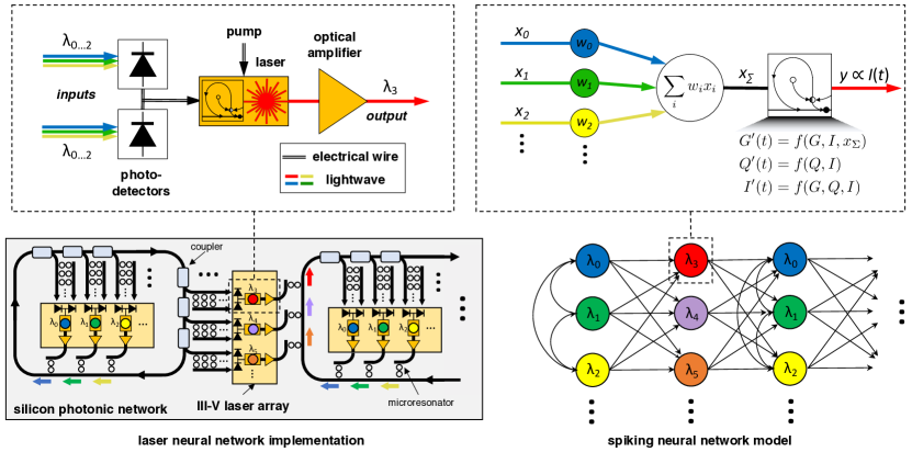
Each laser neuron models the behavior of a simple spiking neuron using optical pulses to code information (for a further discussion on spiking, see the Supplementary materials). As shown in Figure 1, a single processing unit consists of a pair of photodetectors directly wired to the input terminal of a laser, followed by an amplifier. Inputs of multiple wavelengths —in which the intensites are weighted by using a passive silicon network external to each processing unit—are incident on a pair of balanced photodetectors. Excited carriers relax and sum together the input signals, resulting in a current signal proportional to . The resulting push-pull current travels into a laser biased just below threshold. The input acts as a perturbation to the laser’s internal dynamical system , and with enough positive inputs, the laser can excite and fire an optical pulse as the output .
The laser’s dynamical system is represented via the interactions between a gain medium, an absorbing medium, and the light within the cavity. This system performs several nonlinear processing functions on the input data, including integration, thresholding, and time discretization (i.,e., refractoriness) via a mechanism called excitability. A simplified, undimensionalized version of the equations governing this system can be represented by Dubbeldam and Krauskopf (1999):
| (1) | ||||
| (2) | ||||
| (3) |
for gain variable , absorber variable , cavity intensity , and parameters (,,,,,,). As discovered in Ref. Nahmias et al. (2013), under certain conditions, these equations simplify to a model of a Leaky Integrate-and-Fire (LIF) neuron, a popular spiking model in computational neuroscience Koch (1998):
| (4) | ||||
| if then | (5) | |||
| release a pulse, and set . |
Together, a balanced photodetector, laser and amplifier can emulate the basic functions of a spiking neuron. In principle, networks of spiking neurons can perform any algorithm or simulate any nonlinear dynamical system Maass and Bishop (2001).
I.2 Networking

Laser neurons are designed to be compatible with Broadcast-and-Weight (B&W), a reconfigurable optical neural networking method proposed in Ref. Tait et al. (2014). The B&W protocol assigns each laser neuron a unique wavelength . Wavelength division multiplexing (WDM) allows for the aggregation of these signals along common bus waveguides, which distribute the signals with unique transmission profiles to each processing node. Tunable filter banks adjust the strength of each connection, or weightTait et al. (2016, 2018). The resulting weighted signals sum together via the balanced photodetectors (BPDs) driving each laser. This system can implement both negative and positive weights (), allowing for fully reconfigurable neural network models. Coupling to a waveguides in a loop topology allows for recurrent connections, while coupling from one waveguide to another allows for feedforward connections, as illustrated in Fig 1.
In contrast to several other networking frameworks (i.e., coherent matrix multiplication Shen et al. (2017) or optical reservoirs Appeltant et al. (2011); Paquot et al. (2012); Brunner et al. (2013); Vandoorne et al. (2014)), B&W can implement both feedforward and recurrent connections with full tunability. An example of a network including both types is illustrated in Fig. 1 (bottom left), in which two recurrent groups of neurons communicate via a feedforward set of laser neurons. The B&W protocol can also realize more complex and interesting topologies such as hierarchical or small-world networks, as discussed in Ref. Tait et al. (2014); Peng et al. (2018a).
I.3 Fabrication
Each laser neuron consists of III-V photonic devices that can be found in most standard process design kits (PDKs) common to large-scale foundry models: a distributed feedback laser (DFB), a balanced photodetector (BPD) pair, and a semiconductor optical amplifier (SOA). Lithographically-defined metal wires connect the components together in a way that allows for direct interactions between the detectors and the laser. The DFB lasers are composed of electrically pumped multi-quantum wells (MQW) with emission near embedded in a ridge-waveguide structure. The laser includes both a primary gain section as well as a smaller absorber section, with lengths and , respectively. An etched, intracavity electrical isolation section of length divides the two sections, and a small absorber placed on the non-emitting port of each laser reduces back reflections. The SOA also includes an active MQW structure, with a length set to . Device layouts were generated in collaboration with the Fraunhofer Institute for Telecommunications, at the Heinrich Hertz Institute (HHI) as part of the Joint European Platform for Photonic Integration of Components and Circuits (JePPiX) consortium.


II Results
II.1 Multi-Wavelength Functionality
To utilize the dense interconnectivity possible in the B&W protocol, a laser spiking neuron must be able to receive intensity signals with unique wavelengths , and emit a single wavelength . We experimentally demonstrate this functionality together with spiking dynamics, measuring the nonlinear response to both excitatory (positive) and inhibitory (negative) pulses (Fig. 4), and measure the output spectrum for above-threshold signals (Fig. 5). For this experiment, we used a laser neuron unit without amplifier (unit B, as illustrated in Fig. 3).
For simplicity, the experimental demonstration used a total of eight wavelength channels with independent spiking signals: four inputs incident on each photodetector. A topographical micrograph of the device is shown in Fig. 3. The laser current is biased just below the lasing threshold () to initiate the system in a state of excitability. The excitatory photodetector is reversed biased at , whereas the inhibitory photodetector is reversed biased at . As shown in Fig 4(a), the laser neuron only responds with an output pulse if a cluster of excitatory pulses arrives closely spaced in time. This demonstrates several key attributes: summation across multiple wavelengths inputs , the ability to integrate pulse activity across some integration time interval , and the ability to make a binarized (0,1) threshold decision based on input spike activity.
A BPD pair allows for the implementation of both positive and negative weights. Fig 4(b) shows that inhibitory pulses can oppose the activity excitatory pulses: generating a cluster of inhibitory pulses that coincide with the first excitatory cluster results in a cancellation of the output pulse (i.e., via a negative weighting of the inhibitory signals that opposes the positive weighting of the excitatory signals). Another important condition is a well-defined output wavelength, critical for wavelength identification and filtering in the B&W protocol. Fig 5 shows the output spectrum of the laser modulated with excitatory pulses above threshold: it outputs with a stable and narrow linewidth .
Although just eight channels were demonstrated here, the B&W protocol allows for flexible channel scaling through the addition of more wavelengths and laser processing nodes. In B&W networks, two primary limiting factors include the finesse of the passive filters in the network Tait et al. (2016), and the gain bandwidth of the lasers. If high finesse, miniaturized resonators Timurdogan et al. (2014) are combined with a standard III-V laser gain spectrum Arakawa and Yariv (1986) covering the optical C-band, can reach on the order of several hundred channels.
This allows us to characterize the potential processing speed of each laser as a function of the number of wavelength channels . With refractory period , a single laser neuron can make a spike or no-spike decision across inputs every . The number of MACs per second—the speed of each processor—is therefore . With a refractory period Peng et al. (2018b) and (assuming < 3 dB power penalty, see Ref. Tait et al. (2018); Xu, Fattal, and Beausoleil (2008)), we arrive at , or . This speed is quite enormous for a single device, exceeding the total processing capacity of many microelectronic processors. Note that since the speed per node is , it is dependent on channel scalability: higher processing capacity requires a fully-scaled processing system as depicted in Fig. 1 with several hundred wavelength channels per broadcast waveguide.
II.2 Cascadability

An important condition for larger networks is that the nonlinear processors are cascadable. As discussed in Ref. Peng et al. (2018a), signals must be able to propagate through a network without degradation. This divides into both gain cascadability—the ability to drive the next stage of neurons with enough energy—and signal cascadability, the fidelity of the information encoding from one stage to another. In this section, we experimentally demonstrate that a laser spiking neuron can meet a number of cascadability conditions in both domains, and characterize its performance and energy consumption during operation.
We first show that a laser neuron with an amplifier (type A in Fig. 2) can meet the closed-loop gain condition with fixed point precision (see Sec. IV.1 for a discussion on precision). To simulate peak processing conditions, we generate a dense, random stream of excitatory inputs spikes and measure the laser output response. We assume a Poisson point process (a common assumption in spiking signals Gabbiani and Koch (1998)). The probability distribution of , where is the number of spikes that occur on the interval is given by:
| (6) |
We set and defined the input pulse width as over a repeated time interval (see Sec. V.1 for more discussion on experimental conditions). Meeting the closed loop gain condition requires that the optical output power exceeds the input (). We adjusted the SOA input current until the output power exceeds the input by about to account for the projected coupling and microresonator insertion losses in the system. This occured for an SOA current of at . We show time traces of both the input and output in Fig. 6 for this condition.
Secondly, we confirmed that each neuron has nonlinear pulse regeneration capabilities. As discussed in Ref. Peng et al. (2018a), to assure that spikes remain binarized over many stages, nonlinear processors must regenerate pulses as the are incident on each device. We demonstrated pulse width compression and stability (Fig. 6, right): pulses stay approximately constant a full-width half maximum (FWHM) width of . This assures that spikes do not lose their timing characteristics as they propagate forward, maintaining a temporal precision of . The results indicate more than just a simple nonlinearity—input activity (even a square pulse, as shown in Fig. 6) manifests in the output as characteristic pulse with a fairly stable FWHM.
Based on these measurements, we can calculate the energy consumption of each laser processor. The vast majority of dissipation occurs in the amplifier, consuming approximately per node. With a processing speed of , this amounts to per MAC. This is the range of current deep learning hardware (i.e., see comparison in Ref. Peng et al. (2018a)), and depends on a large channel number to realize its advantages. Nonetheless, it is far from the most efficient processing model possible. For example, efficient directly-driven lasers (i.e., lower threshold models Takeda et al. (2013); Wu et al. (2015)) negate the need for an amplifier. Alternatively, to stay compatible with emerging PIC standards, transimpedance amplifiers in platforms with co-integration between electronics and photonics can provide efficient electrical gain between detectors and lasers (many examples of which are provided in Ref. Jeong, Bae, and Jeong (2017)).
III Conclusion
We have demonstrated that a laser neuron, fabricated in a photonic integrated circuit platform, can function as a processing node in a larger scale spiking neural network. Laser neurons communicate photonically, sidestepping many of the costs associated with both data movement and the implementation of linear operations in electronics. This leads to the potential for much higher speeds and energy efficiencies compared to neuromorphic electronic processors. We experimentally validated LIF neuron model functionality across multiple wavelength channels, including the ability to integrate multiple signals together across time, accept both positive (excitatory) and negative (inhibitory) inputs, and make a binary (0,1) spike classification based on pulsed activity. We verified its compatibility with the B&W protocol, assuring that it can utilize the full bandwidth density available to optical waveguides for connectivity. We also demonstrated cascadability, both in the laser neuron’s ability to sustain and amplify signals and its ability to maintain the integrity of pulsed signals from one layer to another.
Our calculated speed and energy efficiencies— per neuron and , respectively—exceed current microelectronic performance figures, particularly in speed. Further developments in optoelectronic devices Miller (2017), co-integration between photonic and electronic platforms Sun et al. (2015); Atabaki et al. (2018), or the utilization of novel materials such as graphene Shastri et al. (2016) provide ample avenues for further exploration. These techniques would realize the potential 3-5 orders-of-magnitude improvements Peng et al. (2018a) that neuromorphic photonic computing has to offer.
IV Supplementary Materials
IV.1 Precision
The precision of each computation, bounded by noise and device variations, limits information capacity. We can define precision with respect to multiply-and-accumulate (MAC) operations: each laser neuron computes a dot product of vector length with bits of precision, giving a total of bits being computed over MAC operations. To avoid processing degradation, cascadability requires that signals with bits of precision stay above some set threshold . In the case of spiking, the amplitude is binary (1 bit of precision), while the spike times should remain analog ( bits of precision for time between spikes for spike and pulse width ). Therefore, laser processors must assure that outputs remain spatially coherent, while preventing a reduction in analog temporal precision by keeping below a threshold value . The lack of this condition can eventually cause pulses to widen, and degrade as they propagate through a network.
MAC operations can either be floating point—in which the quantization threshold is proportional to the output amplitude, as seen in most digital processors—or they can be fixed point, in which the quantization threshold is set independently of the output amplitude. AI researchers have shown that fixed point matrix multiplication can work just as well for deep learning models, even for training Köster et al. (2017). Inference, in particular, does not require high resolution: typically several bits of precision can achieve near state-of-the-art performanceHubara et al. (2016); Courbariaux, Bengio, and David (2015). B&W weight networks best approximate fixed point linear operations, since precision is typically bounded by some physical noise threshold by the signal or reciever. In fixed point arithmetic, a minimum power resolution threshold is set at the detector, and the number of bits of precision for signal is equal to . To prevent degradation, the total signal amplitude from one stage to another must be conserved. Divided individually, a laser neuron must, on average, provide enough gain to compensate for node-to-node losses. In a fixed point framework, the total power required to meet this condition is proportional to the number of processors, , not the number of connections , an advantage that arises from the non-dissipative nature of passive analog operations Shen et al. (2017). If the B&W network remains passive, the closed loop gain condition becomes the most critical source of energy consumption.
IV.2 Optoelectronic Nonlinearities
Researchers have used a variety of implementions to realize nonlinear functions in the optical domain. All-optical approaches have utilized nonlinear effects in both fibers Trillo et al. (1988); Nelson et al. (1991); Asobe (1997) and on-chip resonators Tait (2012); Notomi et al. (2007); Nozaki et al. (2010); Van et al. (2002). Other approaches include carrier nonlinearities in SOAs Sokoloff et al. (1993); Stubkjaer (2000); Vandoorne et al. (2011), plasmonics Ren et al. (2011); Kauranen and Zayats (2012) intracavity semiconductor saturable absorbers Takahashi, Kawamura, and Iwamura (1996); Selmi et al. (2014) and graphene Shastri et al. (2016). However, these approaches consistently exhibit several common limitations: they either require exotic fabrication processes to create, or large optical threshold powers to activate. This can greatly increase the energy consumption to a level that negates the advantages of using optics at all.
Laser neurons use a detector-transducer configuration, a common optoelectronic nonlinear device template explored in the literature Romeira et al. (2016); Krauskopf et al. (2003); Nahmias et al. (2016); Tait et al. (2017); Nozaki et al. (2018). O/E/O models (i.e., involving optical to electrical conversion and vise versa) can exploit nonlinearities in detectors and modulators or lasers, but are constrained by electrical parasitics and the costs of O/E and E/O conversion. However, electro-optic conversion costs are shrinking: high performance detectors Chen and Lipson (2009); Michel, Liu, and Kimerling (2010), modulators Dong et al. (2009); Timurdogan et al. (2014) and lasers Wang et al. (2015); Liu et al. (2015) are continuing to emerge in developing PIC platforms. In addition, placing detectors and transducers in close proximity can greatly minimize undesirable parasitics, including dispersion, microwave reflections, and timing delays Lee (2003).
Another exciting prospect is the close integration between developing microelectronic and photonic platforms, which could combine a high O/E/O conversion efficiency with powerful nonlinear electronic operations. For example, operational amplifiers can be placed after detectors, compensating for loss and leading to greater system-level energy efficiency. Such hybrid units could potentially perform generic nonlinear tasks such as wavelength conversion very efficiently Nozaki et al. (2018) and may provide ample machinery for nonlinear neural network processing in future systems.
IV.3 Spiking
Spiking is a communication encoding strategy that is equivalent to analog pulse position modulation in photonics Smith, Blaikie, and Taylor (1998); Sushchik et al. (2000): information is primarily encoded in the timing between a series of pulses, or spikes. Spike amplitudes are binarized (i.e., either 0 or 1), but the timing of each pulse can take on any analog value. For example, an analog vector can be encoded by associating each value with the time between each pulse, wherein the amount of information encoded is limited by the temporal resolution or timing jitter of the communication system.
Spike encoding has many advantages over continuous wave signals. For one, it is less susceptible to amplitude noise, which can be useful in physical systems with high stochasticity (i.e., biology). Secondly, it benefits from sparse coding, which can lead to significant power advantages for photonic signals. As an illustrative example, for temporal resolution , and delay between pulse and , if , a single pulse can carry more than 1 bit of information: as much as . This reduces the cost by a factor in a communication channel (see for example Ref. Shiu and Kahn (1999)), which can also improve the implementation of operations, such as MACs, in neuromorphic photonic systems.
Unfortunately, although spiking neural networks in hardware have continued to show significant power efficiency gains over other neural network processors Merolla et al. (2014); Furber (2016), they are currently challenging to program and train. Spike-based learning algorithms—such as synaptic time dependent plasticity (STDP)—have difficulty propagating gradients back many layers, a prerequisite condition for deep learning. Nonetheless, improvements in this arena remains an active research topic Pfeiffer and Pfeil (2018), with many results on spiking training appearing recently Samadi, Lillicrap, and Tweed (2017); Kheradpisheh et al. (2018); Tavanaei et al. (2018). As more sophisticated techniques are developed for the control of spiking neural networks, machine learning approaches may one day reap the robustness and energy efficiency that such encoding can deliver.
V Methods
V.1 Experimental Signal Generation

Excitatory and inhibitory pulses were programmed using a custom input generation system, allowing intensity-modulated bit patterns along different wavelengths in some desired test window . As illustrated in Fig. 7, it consisted of a WDM source (an external array of DFB lasers), a single high speed Mach Zehnder (MZ) modulator connected to a pulse pattern generator (PPG) driven by a clock source, and a series of long delay lines nested between arrayed waveguide gratings (AWGs). The outputs were measured by a sampling scope connected to the same clock source. The system has many similarities to the generation mechanisms explored in Ref. Tait et al. (2015); Ferreira de Lima et al. (2016). We describe its mechanism of operation below.
Suppose we have a series of desired bit patterns denoted by along wavelength channels that include bit values programmed in the time interval . First, we set the PPG bit pattern as each desired pattern consecutively in time, i.e.,
for . The total length of the PPG bit pattern is therefore . This pattern is modulated onto all wavelengths using a wideband modulator simultaneously. Next, we send the signal through a Demux AWG and apply consecutive physical time delays to each wavelength channel to cancel out the programmed time delays in the PPG. As a result, we generate our desired pattern in the time interval :
| (7) |
In this experiment, we represented wavelength channels using long fiber delays at intervals of , , etc. Small variations in the physical delay for each fiber (around ) that resulted from splicing errors were compensated for digitally in the PPG delay time, i.e.,
for physically measured delays , where we set the time window to for all channels to avoid overlapping (). The delayed output signals were multiplexed onto two output fibers using another set of AWGs, shown as the excitatory and inhibitory inputs in Fig. 7. Three erbium doped fiber amplifiers (EDFAs) were placed in various parts of the signal pathway to compensate for losses: one after the MZ modulator and before the Demux AWG, and one for each excitatory and inhibitory input channel after each Mux AWG. The resulting fiber channels were input into a V-groove fiber array, which interfaced with both the inputs and output of each laser neuron via spot size converters (SSCs) on the edge of the chip. The output also received amplification via an EDFA to compensate for chip coupling losses.
Before inputs were coupled into the chip, 90:10 couplers were placed after each EDFA, wherein the smaller signals act both as power monitors and as outputs for measurements. Excitatory inputs shown in Fig. 4 were set at , while inhibitory inputs are set at . The output of each spiking laser neuron was measured using both sampling scope (for time-dependent traces in Figs 4 and 6) and a spectrum analyzer (for spectral measurements in Fig 5).
To generate Poisson inputs for the experiments conducted in Sec. II.2, we used only one wavelength input () fed into the excitatory port of a type A neuron. The Poisson model was set with and a clock rate of (each bit has ) over a time window, which was generated a priori before being programmed into the PPG. The result was modulated onto a signal carrier wave at . For both experiments, input and output powers traveling in and out of both the laser and BPD pair were calculated using a power calibration procedure based on the measured losses between the SSCs and fiber V-groove arrays.
V.2 Data Analysis
The powers of time-dependent traces were calibrated using a set of reference traces normalized via continuous wave power measurements. Up to three reference traces existed for each experiment: total excitatory input power, total inhibitory input power, and total laser output power, measured across the entire time window (i.e., ). Once reference traces become normalized to average power measurements, all remaining data sets in the window of interest were calibrated to this reference set. Time-dependent traces for each wavelength and the laser output were measured independently before calibration. This resulted in the final data plot seen in Fig. 5 and Fig. 6 in the main article (for which the latter plot used only one input wavelength channel).
VI Data Availability
The datasets generated during and/or analysed for this experiment are available from the corresponding author on reasonable request.
References
- Amodei and Hernandez (2018) D. Amodei and D. Hernandez, “Ai and compute,” (2018).
- Esmaeilzadeh et al. (2012) H. Esmaeilzadeh, E. Blem, R. St. Amant, K. Sankaralingam, and D. Burger, “Dark Silicon and the End of Multicore Scaling,” IEEE Micro 32, 122–134 (2012).
- ird (2017) “International roadmap for devices and systems 2017 edition,” Tech. Rep. (Institute of Electrical and Electronics Engineers, 2017).
- et al. (2017) N. P. J. et al., “In-datacenter performance analysis of a tensor processing unit,” in 2017 ACM/IEEE 44th Annual International Symposium on Computer Architecture (ISCA) (2017) pp. 1–12.
- Yu (2018) S. Yu, “Neuro-inspired computing with emerging nonvolatile memorys,” Proceedings of the IEEE, Proceedings of the IEEE 106, 260–285 (2018).
- Ielmini and Wong (2018) D. Ielmini and H. S. P. Wong, “In-memory computing with resistive switching devices,” Nature Electronics 1, 333–343 (2018).
- Burr et al. (2017) G. W. Burr, R. M. Shelby, A. Sebastian, S. Kim, S. Kim, S. Sidler, K. Virwani, M. Ishii, P. Narayanan, A. Fumarola, L. L. Sanches, I. Boybat, M. L. Gallo, K. Moon, J. Woo, H. Hwang, and Y. Leblebici, “Neuromorphic computing using non-volatile memory,” Advances in Physics: X 2, 89–124 (2017), https://doi.org/10.1080/23746149.2016.1259585 .
- Ambrogio et al. (2018) S. Ambrogio, P. Narayanan, H. Tsai, R. M. Shelby, I. Boybat, C. di Nolfo, S. Sidler, M. Giordano, M. Bodini, N. C. P. Farinha, B. Killeen, C. Cheng, Y. Jaoudi, and G. W. Burr, “Equivalent-accuracy accelerated neural-network training using analogue memory,” Nature 558, 60–67 (2018).
- Jo et al. (2010) S. H. Jo, T. Chang, I. Ebong, B. B. Bhadviya, P. Mazumder, and W. Lu, “Nanoscale memristor device as synapse in neuromorphic systems,” Nano Letters 10, 1297–1301 (2010).
- Prezioso et al. (2015) M. Prezioso, F. Merrikh-Bayat, B. D. Hoskins, G. C. Adam, K. K. Likharev, and D. B. Strukov, “Training and operation of an integrated neuromorphic network based on metal-oxide memristors,” Nature 521, 61 EP – (2015).
- Bayat et al. (2018) F. M. Bayat, M. Prezioso, B. Chakrabarti, H. Nili, I. Kataeva, and D. Strukov, “Implementation of multilayer perceptron network with highly uniform passive memristive crossbar circuits,” Nature Communications 9, 2331 (2018).
- Miller (2009) D. A. B. Miller, “Device requirements for optical interconnects to silicon chips,” Proceedings of the IEEE 97, 1166–1185 (2009).
- Psaltis, Brady, and Wagner (1988) D. Psaltis, D. Brady, and K. Wagner, “Adaptive optical networks using photorefractive crystals,” Appl. Opt. 27, 1752–1759 (1988).
- Georgas et al. (2011) M. Georgas, J. Leu, B. Moss, C. Sun, and V. Stojanović, “Addressing link-level design tradeoffs for integrated photonic interconnects,” in 2011 IEEE Custom Integrated Circuits Conference (CICC) (2011) pp. 1–8.
- Miller (2017) D. A. B. Miller, “Attojoule optoelectronics for low-energy information processing and communications,” J. Lightwave Technol. 35, 346–396 (2017).
- Agarwal et al. (2016) S. Agarwal, T.-T. Quach, O. Parekh, A. H. Hsia, E. P. DeBenedictis, C. D. James, M. J. Marinella, and J. B. Aimone, “Energy scaling advantages of resistive memory crossbar based computation and its application to sparse coding,” Frontiers in Neuroscience 9, 484 (2016).
- Shen et al. (2017) Y. Shen, N. C. Harris, S. Skirlo, M. Prabhu, T. Baehr-Jones, M. Hochberg, X. Sun, S. Zhao, H. Larochelle, D. Englund, and M. Soljačić, “Deep learning with coherent nanophotonic circuits,” Nature Photonics 11, 441 EP – (2017).
- Prucnal and Shastri (2017) P. R. Prucnal and B. J. Shastri, Neuromorphic Photonics (CRC Press, Taylor & Francis Group, Boca Raton, FL, USA, 2017).
- Walden (1999) R. H. Walden, “Performance trends for analog to digital converters,” IEEE Communications Magazine, IEEE Communications Magazine 37, 96–101 (1999).
- Walden (2008) R. H. Walden, “Analog-to-digital conversion in the early twenty-first century,” Wiley Encyclopedia of Computer Science and Engineering, , 1–14 (2008).
- Tait et al. (2013) A. N. Tait, B. J. Shastri, M. P. Fok, M. A. Nahmias, and P. R. Prucnal, “The dream: An integrated photonic thresholder,” Journal of Lightwave Technology 31, 1263–1272 (2013).
- Notomi et al. (2007) M. Notomi, T. Tanabe, A. Shinya, E. Kuramochi, H. Taniyama, S. Mitsugi, and M. Morita, “Nonlinear and adiabatic control of high-q photonic crystal nanocavities,” Optics Express 15, 17458–17481 (2007).
- Nozaki et al. (2010) K. Nozaki, T. Tanabe, A. Shinya, S. Matsuo, T. Sato, H. Taniyama, and M. Notomi, “Sub-femtojoule all-optical switching using a photonic-crystal nanocavity,” Nature Photonics 4, 477 EP – (2010).
- Van et al. (2002) V. Van, T. A. Ibrahim, K. Ritter, P. P. Absil, F. G. Johnson, R. Grover, J. Goldhar, and P. . Ho, “All-optical nonlinear switching in gaas-algaas microring resonators,” IEEE Photonics Technology Letters, IEEE Photonics Technology Letters 14, 74–76 (2002).
- Ren et al. (2011) M. Ren, B. Jia, J.-Y. Ou, E. Plum, J. Zhang, K. F. MacDonald, A. E. Nikolaenko, J. Xu, M. Gu, and N. I. Zheludev, “Nanostructured plasmonic medium for terahertz bandwidth all-optical switching,” Advanced Materials, Advanced Materials 23, 5540–5544 (2011).
- Kauranen and Zayats (2012) M. Kauranen and A. V. Zayats, “Nonlinear plasmonics,” Nature Photonics 6, 737 EP – (2012).
- Takahashi, Kawamura, and Iwamura (1996) R. Takahashi, Y. Kawamura, and H. Iwamura, “Ultrafast 1.55 m all-optical switching using low-temperature-grown multiple quantum wells,” Applied physics letters 68, 153–155 (1996).
- Prucnal et al. (2016) P. R. Prucnal, B. J. Shastri, T. F. de Lima, M. A. Nahmias, and A. N. Tait, “Recent progress in semiconductor excitable lasers for photonic spike processing,” Advances in Optics and Photonics 8, 228–299 (2016).
- Feldmann et al. (2019) J. Feldmann, N. Youngblood, C. D. Wright, H. Bhaskaran, and W. H. P. Pernice, “All-optical spiking neurosynaptic networks with self-learning capabilities,” Nature 569, 208–214 (2019).
- Peng et al. (2018a) H. Peng, M. A. Nahmias, T. F. de Lima, A. N. Tait, and B. J. Shastri, “Neuromorphic photonic integrated circuits,” IEEE Journal of Selected Topics in Quantum Electronics, IEEE Journal of Selected Topics in Quantum Electronics 24, 1–15 (2018a).
- Peng et al. (2019) H. Peng, G. Angelatos, T. F. de Lima, M. A. Nahmias, A. Tait, S. Abbaslou, B. J. Shastri, and P. Prucnal, “Temporal information processing with an integrated laser neuron,” IEEE Journal of Selected Topics in Quantum Electronics, IEEE Journal of Selected Topics in Quantum Electronics , 1–1 (2019).
- Dubbeldam and Krauskopf (1999) J. L. A. Dubbeldam and B. Krauskopf, “Self-pulsations of lasers with saturable absorber: dynamics and bifurcations,” Optics Communications 159, 325–338 (1999).
- Nahmias et al. (2013) M. A. Nahmias, B. J. Shastri, A. N. Tait, and P. R. Prucnal, “A Leaky Integrate-and-Fire Laser Neuron for Ultrafast Cognitive Computing,” IEEE Journal of Selected Topics in Quantum Electronics 19 (2013).
- Koch (1998) C. Koch, Biophysics of Computation: Information Processing in Single Neurons (Computational Neuroscience) (Oxford University Press, 1998).
- Maass and Bishop (2001) W. Maass and C. M. Bishop, Pulsed neural networks (MIT press, Cambridge, MA, USA, 2001).
- Tait et al. (2014) A. N. Tait, M. A. Nahmias, B. J. Shastri, and P. R. Prucnal, “Broadcast and weight: An integrated network for scalable photonic spike processing,” Journal of Lightwave Technology 32, 3427–3439 (2014).
- Tait et al. (2016) A. N. Tait, A. X. Wu, T. F. de Lima, E. Zhou, B. J. Shastri, M. A. Nahmias, and P. R. Prucnal, “Microring weight banks,” IEEE Journal of Selected Topics in Quantum Electronics 22, 312–325 (2016).
- Tait et al. (2018) A. N. Tait, A. X. Wu, T. F. de Lima, M. A. Nahmias, B. J. Shastri, and P. R. Prucnal, “Two-pole microring weight banks,” Opt. Lett. 43, 2276–2279 (2018).
- Appeltant et al. (2011) L. Appeltant, M. C. Soriano, G. Van der Sande, J. Danckaert, S. Massar, J. Dambre, B. Schrauwen, C. R. Mirasso, and I. Fischer, “Information processing using a single dynamical node as complex system,” Nature Communications 2, 468 (2011).
- Paquot et al. (2012) Y. Paquot, F. Duport, A. Smerieri, J. Dambre, B. Schrauwen, M. Haelterman, and S. Massar, “Optoelectronic reservoir computing,” Scientific Reports 2, 287 EP – (2012).
- Brunner et al. (2013) D. Brunner, M. C. Soriano, C. R. Mirasso, and I. Fischer, “Parallel photonic information processing at gigabyte per second data rates using transient states,” Nature Communications 4, 1364 (2013).
- Vandoorne et al. (2014) K. Vandoorne, P. Mechet, T. Van Vaerenbergh, M. Fiers, G. Morthier, D. Verstraeten, B. Schrauwen, J. Dambre, and P. Bienstman, “Experimental demonstration of reservoir computing on a silicon photonics chip,” Nature Communications 5, 3541 EP – (2014).
- Timurdogan et al. (2014) E. Timurdogan, C. M. Sorace-Agaskar, J. Sun, E. Shah Hosseini, A. Biberman, and M. R. Watts, “An ultralow power athermal silicon modulator,” Nature Communications 5, 4008 EP – (2014).
- Arakawa and Yariv (1986) Y. Arakawa and A. Yariv, “Quantum well lasers–gain, spectra, dynamics,” IEEE Journal of Quantum Electronics, IEEE Journal of Quantum Electronics 22, 1887–1899 (1986).
- Peng et al. (2018b) H.-T. Peng, M. A. Nahmias, T. F. de Lima, A. N. Tait, B. J. Shastri, and P. R. Prucnal, in 2018 IEEE Photonics Conference (IPC) (2018) pp. 1–2.
- Xu, Fattal, and Beausoleil (2008) Q. Xu, D. Fattal, and R. G. Beausoleil, “Silicon microring resonators with 1.5-µm radius,” Optics Express, Optics Express 16, 4309–4315 (2008).
- Gabbiani and Koch (1998) F. Gabbiani and C. Koch, “Principles of spike train analysis,” Methods in neuronal modeling 12, 313–360 (1998).
- Takeda et al. (2013) K. Takeda, T. Sato, A. Shinya, K. Nozaki, W. Kobayashi, H. Taniyama, M. Notomi, K. Hasebe, T. Kakitsuka, and S. Matsuo, “Few-fj/bit data transmissions using directly modulated lambda-scale embedded active region photonic-crystal lasers,” Nature Photonics 7, 569 EP – (2013).
- Wu et al. (2015) S. Wu, S. Buckley, J. R. Schaibley, L. Feng, J. Yan, D. G. Mandrus, F. Hatami, W. Yao, J. Vučković, A. Majumdar, and X. Xu, “Monolayer semiconductor nanocavity lasers with ultralow thresholds,” Nature 520, 69 EP – (2015).
- Jeong, Bae, and Jeong (2017) G.-S. Jeong, W. Bae, and D.-K. Jeong, “Review of cmos integrated circuit technologies for high-speed photo-detection,” Sensors 17 (2017), 10.3390/s17091962.
- Sun et al. (2015) C. Sun, M. T. Wade, Y. Lee, J. S. Orcutt, L. Alloatti, M. S. Georgas, A. S. Waterman, J. M. Shainline, R. R. Avizienis, S. Lin, B. R. Moss, R. Kumar, F. Pavanello, A. H. Atabaki, H. M. Cook, A. J. Ou, J. C. Leu, Y.-H. Chen, K. Asanović, R. J. Ram, M. Popović, and V. M. Stojanović, “Single-chip microprocessor that communicates directly using light,” Nature 528, 534 EP – (2015).
- Atabaki et al. (2018) A. H. Atabaki, S. Moazeni, F. Pavanello, H. Gevorgyan, J. Notaros, L. Alloatti, M. T. Wade, C. Sun, S. A. Kruger, H. Meng, K. Al Qubaisi, I. Wang, B. Zhang, A. Khilo, C. V. Baiocco, M. Popović, V. M. Stojanović, and R. J. Ram, “Integrating photonics with silicon nanoelectronics for the next generation of systems on a chip,” Nature 556, 349–354 (2018).
- Shastri et al. (2016) B. J. Shastri, M. A. Nahmias, A. N. Tait, A. W. Rodriguez, B. Wu, and P. R. Prucnal, “Spike processing with a graphene excitable laser,” Scientific Reports 6, 19126 EP – (2016).
- Köster et al. (2017) U. Köster, T. Webb, X. Wang, M. Nassar, A. K. Bansal, W. Constable, O. Elibol, S. Gray, S. Hall, L. Hornof, A. Khosrowshahi, C. Kloss, R. J. Pai, and N. Rao, “Flexpoint: An adaptive numerical format for efficient training of deep neural networks,” in Advances in Neural Information Processing Systems 30, edited by I. Guyon, U. V. Luxburg, S. Bengio, H. Wallach, R. Fergus, S. Vishwanathan, and R. Garnett (Curran Associates, Inc., 2017) pp. 1742–1752.
- Hubara et al. (2016) I. Hubara, M. Courbariaux, D. Soudry, R. El-Yaniv, and Y. Bengio, “Binarized neural networks,” in Advances in Neural Information Processing Systems 29, edited by D. D. Lee, M. Sugiyama, U. V. Luxburg, I. Guyon, and R. Garnett (Curran Associates, Inc., 2016) pp. 4107–4115.
- Courbariaux, Bengio, and David (2015) M. Courbariaux, Y. Bengio, and J.-P. David, “Binaryconnect: Training deep neural networks with binary weights during propagations,” in Advances in Neural Information Processing Systems 28, edited by C. Cortes, N. D. Lawrence, D. D. Lee, M. Sugiyama, and R. Garnett (Curran Associates, Inc., 2015) pp. 3123–3131.
- Trillo et al. (1988) S. Trillo, S. Wabnitz, E. M. Wright, and G. I. Stegeman, “Soliton switching in fiber nonlinear directional couplers,” Opt. Lett. 13, 672–674 (1988).
- Nelson et al. (1991) B. P. Nelson, K. J. Blow, P. D. Constantine, N. J. Doran, J. K. Lucek, I. W. Marshall, and K. Smith, “All-optical gbit/s switching using nonlinear optical loop mirror,” Electronics Letters, Electronics Letters 27, 704–705 (1991).
- Asobe (1997) M. Asobe, “Nonlinear optical properties of chalcogenide glass fibers and their application to all-optical switching,” Optical Fiber Technology 3, 142–148 (1997).
- Tait (2012) A. N. Tait, The Dual Resonator Enhanced Asymmetric Mach-Zehnder Interferometer: An Ultrafast Thresholder for Integrated Photonic Platforms, Undergraduate thesis, Princeton University (2012).
- Sokoloff et al. (1993) J. P. Sokoloff, P. R. Prucnal, I. Glesk, and M. Kane, “A terahertz optical asymmetric demultiplexer (toad),” IEEE Photonics Technology Letters, IEEE Photonics Technology Letters 5, 787–790 (1993).
- Stubkjaer (2000) K. E. Stubkjaer, “Semiconductor optical amplifier-based all-optical gates for high-speed optical processing,” IEEE Journal of Selected Topics in Quantum Electronics, IEEE Journal of Selected Topics in Quantum Electronics 6, 1428–1435 (2000).
- Vandoorne et al. (2011) K. Vandoorne, J. Dambre, D. Verstraeten, B. Schrauwen, and P. Bienstman, “Parallel reservoir computing using optical amplifiers,” IEEE Transactions on Neural Networks, IEEE Transactions on Neural Networks 22, 1469–1481 (2011).
- Selmi et al. (2014) F. Selmi, R. Braive, G. Beaudoin, I. Sagnes, R. Kuszelewicz, and S. Barbay, “Relative refractory period in an excitable semiconductor laser,” Physical Review Letters 112, 183902 (2014).
- Romeira et al. (2016) B. Romeira, R. Avó, J. L. Figueiredo, S. Barland, and J. Javaloyes, “Regenerative memory in time-delayed neuromorphic photonic resonators,” Scientific Reports 6, 19510 EP – (2016).
- Krauskopf et al. (2003) B. Krauskopf, K. Schneider, J. Sieber, S. Wieczorek, and M. Wolfrum, “Excitability and self-pulsations near homoclinic bifurcations in semiconductor laser systems,” Optics Communications 215, 367–379 (2003).
- Nahmias et al. (2016) M. A. Nahmias, A. N. Tait, L. Tolias, M. P. Chang, T. Ferreira de Lima, B. J. Shastri, and P. R. Prucnal, “An integrated analog o/e/o link for multi-channel laser neurons,” Applied Physics Letters 108, 151106 (2016).
- Tait et al. (2017) A. N. Tait, T. F. de Lima, E. Zhou, A. X. Wu, M. A. Nahmias, B. J. Shastri, and P. R. Prucnal, “Neuromorphic photonic networks using silicon photonic weight banks,” Scientific Reports 7, 7430 (2017).
- Nozaki et al. (2018) K. Nozaki, S. Matsuo, T. Fujii, K. Takeda, E. Kuramochi, A. Shinya, and M. Notomi, “Ultracompact o-e-o converter based on ff-capacitance nanophotonic integration,” in Conference on Lasers and Electro-Optics (Optical Society of America, 2018) p. SF3A.3.
- Chen and Lipson (2009) L. Chen and M. Lipson, “Ultra-low capacitance and high speed germanium photodetectors on silicon,” Optics Express 17, 7901–7906 (2009).
- Michel, Liu, and Kimerling (2010) J. Michel, J. Liu, and L. C. Kimerling, “High-performance ge-on-si photodetectors,” Nature Photonics 4, 527 EP – (2010).
- Dong et al. (2009) P. Dong, S. Liao, D. Feng, H. Liang, D. Zheng, R. Shafiiha, C.-C. Kung, W. Qian, G. Li, X. Zheng, A. V. Krishnamoorthy, and M. Asghari, “Low vpp, ultralow-energy, compact, high-speed silicon electro-optic modulator,” Opt. Express 17, 22484–22490 (2009).
- Wang et al. (2015) Z. Wang, B. Tian, M. Pantouvaki, W. Guo, P. Absil, J. Van Campenhout, C. Merckling, and D. Van Thourhout, “Room-temperature inp distributed feedback laser array directly grown on silicon,” Nature Photonics 9, 837 EP – (2015).
- Liu et al. (2015) A. Y. Liu, S. Srinivasan, J. Norman, A. C. Gossard, and J. E. Bowers, “Quantum dot lasers for silicon photonics [invited],” Photon. Res. 3, B1–B9 (2015).
- Lee (2003) T. H. Lee, The Design of CMOS Radio-Frequency Integrated Circuits, 2nd ed. (Cambridge University Press, 2003).
- Smith, Blaikie, and Taylor (1998) E. D. J. Smith, R. J. Blaikie, and D. P. Taylor, “Performance enhancement of spectral-amplitude-coding optical cdma using pulse-position modulation,” IEEE Transactions on Communications, IEEE Transactions on Communications 46, 1176–1185 (1998).
- Sushchik et al. (2000) M. Sushchik, N. Rulkov, L. Larson, L. Tsimring, H. Abarbanel, K. Yao, and A. Volkovskii, “Chaotic pulse position modulation: a robust method of communicating with chaos,” IEEE Communications Letters, IEEE Communications Letters 4, 128–130 (2000).
- Shiu and Kahn (1999) D.-S. Shiu and J. M. Kahn, “Differential pulse-position modulation for power-efficient optical communication,” IEEE Transactions on Communications, IEEE Transactions on Communications 47, 1201–1210 (1999).
- Merolla et al. (2014) P. A. Merolla, J. V. Arthur, R. Alvarez-Icaza, A. S. Cassidy, J. Sawada, F. Akopyan, B. L. Jackson, N. Imam, C. Guo, Y. Nakamura, B. Brezzo, I. Vo, S. K. Esser, R. Appuswamy, B. Taba, A. Amir, M. D. Flickner, W. P. Risk, R. Manohar, and D. S. Modha, “A million spiking-neuron integrated circuit with a scalable communication network and interface,” Science 345, 668–673 (2014), http://science.sciencemag.org/content/345/6197/668.full.pdf .
- Furber (2016) S. Furber, “Large-scale neuromorphic computing systems,” Journal of Neural Engineering 13, 051001 (2016).
- Pfeiffer and Pfeil (2018) M. Pfeiffer and T. Pfeil, “Deep learning with spiking neurons: Opportunities and challenges,” Frontiers in neuroscience 12, 774; 774–774 (2018).
- Samadi, Lillicrap, and Tweed (2017) A. Samadi, T. P. Lillicrap, and D. B. Tweed, “Deep learning with dynamic spiking neurons and fixed feedback weights,” Neural Computation, Neural Computation 29, 578–602 (2017).
- Kheradpisheh et al. (2018) S. R. Kheradpisheh, M. Ganjtabesh, S. J. Thorpe, and T. Masquelier, “Stdp-based spiking deep convolutional neural networks for object recognition,” Neural Networks 99, 56 – 67 (2018).
- Tavanaei et al. (2018) A. Tavanaei, M. Ghodrati, S. R. Kheradpisheh, T. Masquelier, and A. S. Maida, “Deep learning in spiking neural networks,” arXiv preprint arXiv:1804.08150 (2018).
- Tait et al. (2015) A. N. Tait, J. Chang, B. J. Shastri, M. A. Nahmias, and P. R. Prucnal, “Demonstration of WDM weighted addition for principal component analysis,” Optics Express 23, 12758–12765 (2015).
- Ferreira de Lima et al. (2016) T. Ferreira de Lima, A. N. Tait, M. A. Nahmias, B. J. Shastri, and P. R. Prucnal, “Scalable Wideband Principal Component Analysis via Microwave Photonics,” IEEE Photonics Journal In press (2016).