Charge and spin transport over record distances in GaAs metallic n-type nanowires : I photocarrier transport in a dense Fermi sea
Abstract
We have investigated charge and spin transport in n-type metallic GaAs nanowires ( cm-3 doping level), grown by hydride vapor phase epitaxy (HVPE) on Si substrates. This was done by exciting the nanowire by tightly-focussed circularly-polarized light and by monitoring the intensity and circular polarization spectrum as a function of distance from the excitation spot. The spin-polarized photoelectrons give rise to a well-defined feature in the nearbandgap spectrum, distinct from the main line due to recombination of the spin-unpolarized electrons of the Fermi sea with the same minority photoholes. At a distance of 2 m, only the main line remains, implying that photoelectrons have reached a charge thermodynamic equilibrium with the Fermi sea. However, although no line is present in the intensity spectrum at the corresponding energy, the circular polarization is still observed at the same energy in the spectrum, implying that photoelectrons have preserved their spin orientation and that the two spin reservoirs remain distinct. Investigations as a function of distance to the excitation spot show that, depending on excitation power, a photoelectron spin polarization of can be transported over a record distance of more than 20 m. This finding has potential applications for long distance spin transport in n-type doped nanowires.
I Introduction
The investigation of transport in systems of reduced dimensionality such as nanowires (NWs) is of interest both for fundamental reasons and for applications to solar cells Krogstrup et al. (2013), lasers Duan et al. (2003), quantum computing van den Berg et al. (2013) and spintronics Krogstrup et al. (2013); Duan et al. (2003); van den Berg et al. (2013). In silicon, time-resolved experiments have shown that photocarriers can be transported over m Gabriel et al. (2013). For GaAs, the largest charge diffusion length is of 4 m at LT in quantum NWs Nagamune et al. (1995). However, most reported values at LT Bolinsson et al. (2011); Darbandi and Watkins (2016); Gustafsson et al. (2010); Spirkoska et al. (2009) and RT Gutsche et al. (2012) are in the submicron range. Finally, spin transport has to our knowledge been little investigated.
N-type GaAs NWs on the metallic side of the Mott transition appear as a promising system for spin transport because of the large spin lifetime Dzhioev et al. (2002); Romer et al. (2010). The efficiency of the Dyakonov-Perel process, which has been shown to be dominant at this doping level, is likely to be further reduced if the axial NW direction is 111, since the latter process is inefficient if the vector lies along 111 D’yakonov and Perel (1971).
At this doping level, there appear tails in the valence and conduction band, due to statistical fluctuations of donor concentration Efros et al. (1972); Shklovskii and Efros (1984); Borghs et al. (1989). It has been predicted that disorder in one dimensional semiconducting systems can lead to freezing of the spin relaxation Echverria-Arondo and Sherman (2012). On the other hand, it may be believed that the resulting potential fluctuations induce a localization of minority carriers and therefore strongly reduce the distance over which minority carriers can be transported.
In the present work and in its companion paper, hereafter refered to as [II], we use metallic NWs of cm-3 doping level, of exceptional quality and length, produced using Hydride Vapor Phase Epitaxy Ramdani et al. (2010); Gil et al. (2014); Hijazi et al. (2019). IN order to investigate charge and spin transport along the NW, this NW is excited by a tightly-focussed circularly-polarized laser and the evolution of the luminescence emission spectrum and its polarization are monitored at 6K with spatial resolution along the NW. This allows us to investigate charge and spin transport along the NW. As shown before Cadiz et al. (2014), this approach has similarities with time-resolved luminescence investigations Redfield et al. (1970), but is more appropriate to describe charge and spin transport.
Metallic GaAs NW are potentially ideal candidates for charge and spin transport because of two distinct mechanisms, which have been little investigated in the past. Firstly, it will be shown in [II] that charge can be transported in the bandtails over lengths as large as 20 m because of the presence of large internal electric fields of ambipolar origin. Secondly, in the present paper, we investigate, as performed before for bulk materials Knox et al. (1988) and heterostructures Brill and Heiblum (1994), to what level the presence of a Fermi sea of spin-unpolarized intrinsic electrons affects charge and spin transport in the NW. It is shown that thermodynamic equilibrium between photoelectrons and the Fermi sea is established after a small distance of 2 m, but that the two spin reservoirs remain distinct up to 20 m.
This conclusion is reached using a spatially-resolved investigation of the luminescence and polarization spectra. Besides the main emission, due to recombination of photoholes with the Fermi sea, a narrow polarized feature is found corresponding to recombination of spin-polarized photoelectrons lying near the Fermi level with the same photoholes. This line disappears within a distance of 2 m from the excitation spot, thus revealing the establishment of equilibrium between the charge reservoirs of photoelectrons and intrinsic electrons. At the same energy in the spectrum, the circular polarization is still present up to the maximum distance of 2 m, revealing that spin equilibrium has not been reached. Moreover, spatially-resolved investigation of the luminescence degree of circular polarization shows that spin orientation can be transported up to the maximum distance of 20 m, thus revealing spin transport over record lengths. At this distance, depending on excitation power, the photoelectrons can have a spin polarization as large as . This shows the potential interest of the present NW for spin transport.
This paper is organized as follows. The following section is dedicated to a theoretical background and to the experimental details. In Sec. III, the spatially-resolved luminescence and polarization spectra are presented. These results are interpreted in Sec. IV.
II Principles
II.1 NW growth and preparation
Here, we study gold-catalyzed NWs, HVPE-grown on Si(111) substrates at 715 ∘C. These NWs have a length of several tens of m and are characterized by a pure zinc blende structure, free of polytypism and cristalline defects Ramdani et al. (2010); Gil et al. (2014). Since the HCl flux injected inside the reactor produces SiCl4 which acts as a doping precursor, the NW have a donor doping level in the low cm-3 range, weakly dependent on NW diameter Hijazi et al. (2019). This value is about one order of magnitude larger than the one of the Mott transition Benzaquen et al. (1987); Cutler and Mott (1969); Anderson (1958). This value has been obtained from an analysis of the shape of the luminescence spectrum and by Raman analysis Goktas et al. (2018) and has been confirmed using a mapping of the luminescence intensity, leading to the conclusion that the surface depletion layer has a thickness of the order of 90 nm (see supplementary material).
Immediately after growth, the NW were introduced without air exposure into a UHV chamber and were treated at 300K by a nitrogen plasma produced by a commercial electron cyclotron resonance source (SPECS MPS-ECR) operating in atom mode at a pressure of mbar and described elsewhere Mehdi et al. (2018). In order to obtain a homogeneous nitridation on the NW surface, the angle between the source and the substrate surface was kept at 45∘ for 1h and at -45∘ for 1h. This method enables to produce a thin layer of nitride at the GaAs surface which reduces the surface oxidation under air exposure and the surface recombination velocity Mehdi et al. (2019); André et al. (2020).
The NWs, standing on the substrate, were mechanically deposited horizontally on a grid of lattice spacing 15 m. An optical microscope was used to note the coordinates of the individual NW. As found by scanning electron microscopy, the NW used here had a length of m and a diameter of nm.
II.2 Background on luminescence of metallic n-type GaAs
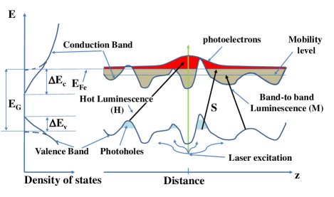
Shown in the right panel of Fig. 1 are the spatial potential fluctuations of the bottom of the conduction band and of the top of the valence band for n-type metallic GaAs. These fluctuations originate from statistical fluctuations of the donor concentration. In a sphere of radius , the statistical fluctuation of the mean number of donors N, given by , is , so that the potential fluctuation is where is the static dielectric constant, is the permittivity of vacuum and is the absolute value of the electronic charge Efros et al. (1972). The potential fluctuations are screened by mobile carriers. Within the Thomas Fermi (TF) 3D model the screening concerns fluctuations of extension larger than where is the donor Bohr radius De-Sheng et al. (1982); Lanyon and Tuft (1979); not (a).
Calculations of the energy dependence of the conduction and valence band densities of states have been performed in the past Lowney (1986). For cm-3 range, one merely observes a broadening of the donor band. In contrast, for the present doping level cm-3, the fluctuations generate a tail lying lower than the conduction band ( see left panel of Fig. 1). The amplitude of this tail has been found of the order of , i. e. comparable with the donor binding energy, while the density of states increases linearly as a function of energy with respect to the bottom of the tail Lowney (1986). Conversely, the valence band also exhibits a tail of amplitude meV, with a density of states increasing also linearly with increasing energy with respect to the top of the tail .
It has been found that the dynamic properties of the two types of carriers in the fluctuations are very different Levanyuk and Osipov (1981); Arnaudov et al. (1977). Under light excitation, the electronic reservoir is characterized by a thermodynamic equilibrium defined by a quasi Fermi level since, because of the small electronic mass, electronic diffusion by tunnel processes from one well to the other one is quite efficient. On the other hand, photoholes tend to get trapped in the potential wells, since relaxation of their kinetic energy occurs in a short characteristic time of 1 ps Chébira et al. (1992); Bimberg et al. (1985), where tunneling processes are less probable because of their large effective mass. As a result, as verified experimentally Redfield et al. (1970), the holes cannot be described by a thermal equilibrium, but by a balance between thermalization and recombination. The valence band levels are occupied by holes with an occupation probability given by
| (1) |
Here is the capture probability of a hole, is the probability for recombination with electrons and is a Fermi function of with an effective Fermi energy given by
| (2) |
Here and are the concentrations of photoelectrons and intrinsic electrons, is the hole concentration and is the valence band effective density of states. The approximate expression is valid at low excitation power, for which and . The hole distribution differs from a Fermi one because of the concentration dependence of the prefactor in Eq. 1. It has been proposed that, because of the large recombination probability of holes at the top of the fluctuations, the hole energy distribution is narrow and peaks at some intermediate kinetic energy De-Sheng et al. (1982); Arnaudov et al. (1977).
The luminescence intensity at energy of the main line, due to recombination between photoholes and intrinsic electrons, is proportional to
| (3) |
with and where k-conservation does not occur because of disorder De-Sheng et al. (1982). Here is the electron occupation probability and is the recombination probability. Expressions of these quantities have been given in Ref Levanyuk and Osipov (1981), which reports a calculation of the shape of the luminescence spectrum.
At a given radial position and axial position in the NW, the intensity, obtained by integration of Eq. 3 over energy , is of the form
| (4) |
where is the bimolecular recombination constant. In the same way, the intensity of the emission due to recombination between photoelectrons and photoholes is
| (5) |
where is the corresponding bimolecular recombination constant. The detected luminescence intensity at a given axial position along the NW is obtained by averaging over the radial coordinate .
The luminescence spectrum may also contain features due to distinct recombination processes. Several works have reported a composite structure of the nearbandgap emission, attributed to a residual excitonic signal De-Sheng et al. (1982) or to band-to-band recombination, while the main line is attributed to donor-related recombination Lee et al. (1996). Independently, it has been shown that, because of screening of the electron-hole interaction, excitons cannot exist for the present doping level, since the exciton absorption peak disappears for Shah et al. (1977). However, it has been shown that biexcitons can survive the Mott transition Shahmohammadi et al. (2014).
II.3 Experimental
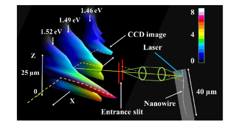
The experimental setup is sketched in Fig. 2. The excitation light is a tightly-focused, continuous-wave, laser beam (Gaussian radius m, energy eV). The luminescence light is focused on the entrance slit of a spectrometer equipped with a CCD camera as a detector. For a n-type material, the band-to-band emission is dominated by recombination of minority photoholes with intrinsic electrons. For spatially-resolved spectral analysis, one monitors the image from the CCD detector. A typical image, taken for a NW temperature of 6K, is shown in Fig. 2 for an excitation power of 9 W not (b). Here, the NW is adjusted so that its image by the detection optics is parallel to the spectrometer entrance slit (axis Z). Thus, section of the image along the perpendicular axis X gives the luminescence spectrum at the corresponding position on the NW. As shown in Fig. 2, the spatial profiles extend well beyond the zone of optical excitation ( m), so that the monitoring of the spectra as a function of distance gives information on evolution of the photocarrier charge and spin reservoirs during transport away from the excitation spot.
Liquid crystal modulators were used to circularly-polarize the excitation laser (-helicity), in order to generate spin-polarized photoelectrons and to selectively detect the intensity of the luminescence components with helicity. Since photoholes as well as intrinsic electrons are spin-unpolarized, the band-to-band luminescence is expected to be also circularly-unpolarized. Conversely, for recombination with spin-polarized photoelectrons, one monitors the difference signal
| (6) |
where for - polarized excitation. This signal is related to the photoelectron spin density , where are the concentrations of photoelectrons with spin , choosing the direction of light excitation as the quantization axis. Finally, the ratio is defined as the degree of circular polarization of the luminescence and is .
III Spatially-resolved sum and difference spectra
III.1 Spectral analysis at the excitation spot
The luminescence image shown in Fig. 2 consists in three bands. Besides the nearbandgap luminescence near 1.52 eV, the band related at 1.49 eV is due to residual carbon acceptors Kisker et al. (1983); Skromme and Stillman (1984). The band near 1.46 eV, possibly caused by carbon acceptors perturbed by nitrogen atoms originating from the surface passivation Leymarie (1989); Ruhstorfer et al. (2020) has properties very close to the former one. The bottom panel of Fig. 3 shows, in logarithmic units, the luminescence intensity spectra at for increasing excitation powers (Curves a, b and c, corresponding to 9 W, 45 W and 180 W respectively) and the spectrum for an excitation power of 180 W but for m (Curve d).
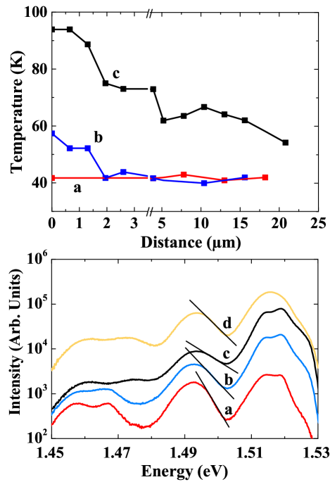
We first consider the acceptor emission at 1.492 eV. The lineshape does not seem to be affected by disorder. As realized earlier De-Sheng et al. (1982); Levanyuk and Osipov (1981), this is because of the relatively small value of the acceptor Bohr radius, so that disorder causes a negligible broadening. It has also been shown that the acceptor luminescence originates from recombination of electrons at the Fermi level, so that the shift of the acceptor emission because of disorder, of Levanyuk and Osipov (1981), is very small not (c). The high-energy slope of the corresponding peak increases with excitation power (Curves a-c of Fig. 3) and becomes smaller at m (Curve d). As already recognized before Ulbrich et al. (1989); Weisbuch (1977), this slope is related to the electron temperature which is, in the present case, the temperature of the Fermi sea. A fit of this line with a shape of the form exp directly gives . The top panel shows the corresponding spatial profiles of . At very low power, and is, as expected, independent on distance. The temperature at increases with excitation power, as seen from a comparison between Curves a, b, and c. Fora power of 180 W, which is the highest power at which the line can be resolved from the nearbandgap emission (Curve c), can be as large as 95K at the place of excitation. In this case, as seen in Curve d, decreases with distance to the excitation spot.
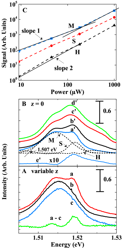
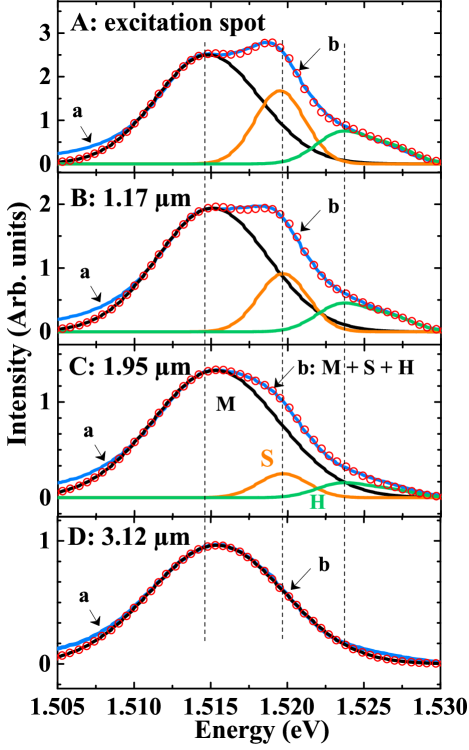
The nearbandgap normalized luminescence intensity spectra at are shown in Panel B of Fig. 4 for selected excitation powers. These spectra are composed of a main line near 1.515 eV labelled M, of a shoulder at 1.519 eV labelled S and of a high-energy tail, above 1.52 eV, labelled H. Curve e’ of Panel B shows the difference spectrum for the smallest excitation power of 9 W. One sees that the polarization of line M is small, so that this line is due to recombination of spin-unpolarized photoholes with intrinsic electrons. Indeed, because of band filling, electrons lying below the Fermi level cannot be spin-polarized. Conversely, lines S and H are polarized and are therefore due to recombination of spin-polarized photoelectrons at the photoelectron quasi-Fermi level and above this level, respectively.
For quantitative analysis, the spectra were decomposed into elementary contributions, as shown for Curve a’ of Panel B of Fig. 4. Line S was fitted by a gaussian component of half-width 2.3 meV and peak energy 1.5195 eV. The width of line S is relatively small since this line reflects the joint widths of the photoelectron distribution, determined by the temperature and of the photohole distributions which, as shown in Sec. IIB, is relatively narrow. The position of line S, which corresponds to the difference between electron quasi-Fermi level and the hole energy, is found to depend very weakly on excitation power, in agreement with the expression of , given by Eq. 2 at weak excitation power. For line M, one has used a gaussian shape of half width meV, i. e. comparable with values measured elsewhere on Si-doped NWs Ruhstorfer et al. (2020). Line M is broader than line S, since its width is determined by the width of the Fermi sea, of the order of the electron Fermi energy. Line M is extrapolated at low energy to a value of 1.507 eV, in relatively good agreement with the value of 1.503 eV expected from Ref. Lowney (1986) for this doping level. Finally, the hot photoelectron contribution H was taken as the residual signal, obtained by subtracting components S and M from the experimental profile. The shape of this component was found to depend weakly on excitation power.
Shown in Panel C of Fig. 4 are the power dependences of the integrated intensities of lines M, S and H. As expected, the intensity of line M is proportional to the excitation power, because of the linear dependence of on excitation power in Eq. (4) (monomolecular recombination). Conversely, that of line H is proportional to its square, since in Eq. (5), both and increase with excitation power (bimolecular recombination). Note that the exponent of the increase of the intensity of line S, of 1.4, is slightly smaller than the value of 2 expected from Eq. (5). This departure may be due to a power dependence of or to the fact that a power-dependent fraction of the photoelectrons is already incorporated into the Fermi sea at .
III.2 Intensity spectra for selected distances to the excitation spot
Fig. 5 shows the intensity spectra for an excitation power of W and for selected distances to the excitation spot. These spectra were decomposed into the elementary contributions of lines M, S and H, in the same way as for Curve a’ of Fig. 4, and the spatial profiles of line S are shown in Fig. 6 for several excitation powers. Fig. 5 shows that line S disappears over a characteristic distance of m so that the spectrum shown in Panel D mostly exhibits line M, with a weak residual H signal above 1.52 eV. The decay is slower than that of the laser spatial profile, shown in Curve d of Fig. 6, implying that the changes in these spectra are not directly related to the photocarrier creation rate but to evolution of the photocarrier system during transport.
Quite generally, the disappearance of line S can be attributed to a nonlinear effect caused by the decrease of photocarrier concentration (note the decrease of the emission intensity by a factor of 3 between Panels A and D of Fig. 5), or to the effect of transport on the photocarrier system. In order to test the sole effect of distance to the excitation spot, we compare in the bottom panel of Fig. 4 the intensity spectra as a function of distance, where for each distance the excitation power was adjusted in such a way that the emission intensity and therefore the carrier concentrations are constant. Curve a is identical to Curve a’ of Panel B, taken at and for the smallest excitation power of 9 W. Curves b’ and c’ are taken for distances of m and m but for excitation powers of 45 W and 180 W, respectively.
As seen from the difference between the spectrum at the excitation spot (Curve a) and the spectrum taken at m (Curve c), the intensities of lines H and M are quite similar between Curves a, b, and c, implying that they are related to the photocarrier concentrations rather than to the distance from the excitation spot. In contrast, line S is absent from Curve b and Curve c of Fig. 4 so that its relative magnitude depends on the distance to the excitation spot rather than on the photocarrier concentration. This allows us to exclude, at variance with earlier work De-Sheng et al. (1982); Lee et al. (1996); Shahmohammadi et al. (2014), electronic species such as excitons, biexcitons as the origin of line S, since in this case the magnitude of this line should mostly depend on carrier concentration and therefore on the intensity of line M. These results rather show the relevance of irreversible establishment of equilibrium occuring after generation of electron-hole pairs during transport away from the excitation spot. This equilibrium concerns the photoelectron gas since since the hole energy relaxation time is quite short and smaller than 1ps Chébira et al. (1992) and since establishment of equilibrium among the hole gas would also affect line M.
III.3 Difference and polarization spectra for increasing distances to the excitation spot
Fig. 7 shows the difference spectra in the same conditions as Fig. 5 as well as, for each distance, the polarization spectra. It is seen that, at large distance, there persists a significant S line in the difference spectrum although no specific feature is detected in the corresponding intensity spectrum. This finding implies that, in spite of the establishment of a charge equilibrium, the photoelectrons and intrinsic electrons still form two distinct spin reservoirs. The persistence of a significant Fermi edge spin polarization at large distance reveals the weakness of the spin relaxation processes Dzhioev et al. (2002).
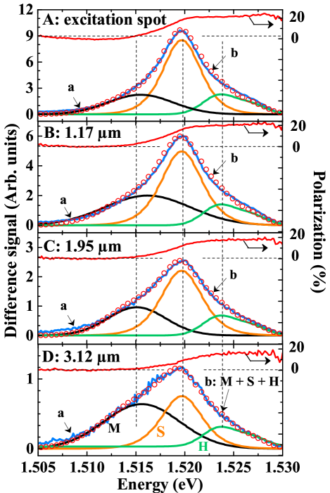
It is then assumed that each photoelectron spin reservoir, of spin , has reached an internal equilibrium characterized by a Fermi energy , such that , in order to ensure charge equilibrium. Developing the function to first order in and dividing by the electron concentration, one finds that the polarization is proportional to . The polarization spectrum in Panel D can be perfectly approximated by , from which we find that the difference between the electron quasi-Fermi energy and the hole energy is of 1.5195 eV. The fact that this energy coincides with the energy of line S is a further confirmation that this line is due to recombination of photoelectrons at the quasi Fermi level.
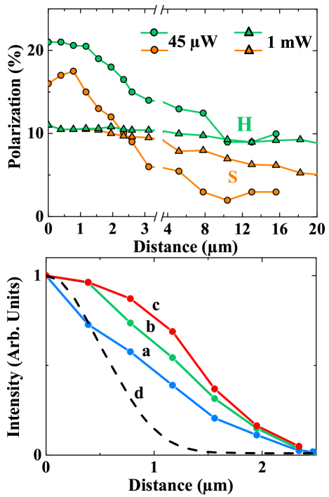
For analysis of the polarization spatial profiles of lines S and H beyond m, it was chosen to monitor the values in the polarization spectra at the respective energies of the peaks of the two lines. This procedure enables to determine the profiles independently of decomposition of the sum and difference spectra up to the maximum distance of m even if no line S is present in the intensity spectrum. The resulting polarization spatial profiles are shown in the top panel of Fig. 6. At the excitation spot and for the smallest excitation power, the luminescence polarization for hot electrons and to some extent for Fermi edge electrons is close to the maximum value of without losses by spin relaxation. For the maximum excitation power, the polarization of line H is . This polarization keeps the same value independently on distance, while the polarization of Fermi edge electrons slowly decreases with distance and is for m. For a reduced excitation power of 45 W, the polarization of line H of , decreases to , these values being and for line S. For the smaller excitation power, in agreement with Fig. 6, the polarization of line S stays larger than up to m, and subsequently decreases to for m.
In summary, it has been found that spin transport can occur over record lengths, with a luminescence polarization of at m for hot photoelectrons. For Fermi edge photoelectrons, spin transport occurs over similar distances, but the polarization losses are larger, in particular for a small excitation power. Even for a low excitation power, polarization of Fermi edge electrons is larger than up to m, at which charge equilibrium with the unpolarized Fermi sea is established.
IV Discussion
In order to outline the physical process at the origin of the experimental effects, we first estimate the order of magnitude of the time for transport out of the laser spot. Taking a typical value of the diffusion constant of cm Cadiz et al. (2014), one finds that this time , is of the order of several tens of ps. In the same way, with the excitation power used for Fig. 5, we estimate that the photocarrier concentration at the excitation spot is of the order of cm -3. Although this estimate is very approximate, it allows us to conclude that the photocarrier concentration is much smaller than the doping level.
IV.1 Establishment of charge equilibrium
The first dynamic process which occurs after creation of an electron in the conduction band is emission of an optical phonon. This emission has been found to occur in a time of ps i. e. significantly smaller than the time for establishment of the equilibrium Kash et al. (1985). Although this time may be larger at high excitation power because of screening of the electron-phonon interaction Seymour and Alfano (1980), the observation of a significant S signal at suggests that emission of optical phonons is complete before diffusion out of the excitation spot.
Electron-electron collisions are also known to enable efficient establishment of equilibrium among the electron gas. The time for collisions between electrons has been calculated including screening by an electron hole plasma and found smaller than 1ps independently on concentration and temperature Binder et al. (1992). Thus it may be believed that establishment of equilibrium among photoelectrons occurs before they leave the excitation spot.
The present experimental results show that, in contrast, equilibrium between the photoelectrons and Fermi edge intrinsic electrons only occurs after a distance of m. Experimentally, the time for establishment of equilibrium between photoelectrons and a Fermi sea of electrons has been found to be shorter than 30 fs. However, this was found in a modulation-doped structure i.e. without screening by charged donors Knox et al. (1988). The slower establishment of equilibrium with the Fermi sea is consistent with the experimental finding that the interaction between photoelectrons and the Fermi sea, rather than occuring through single particle processes, modifies the equilibrium of the overall Fermi sea Brill and Heiblum (1994). This suggests that, at the excitation spot, the equilibrium of the photoelectron reservoir may be a Boltzmann-like with a temperature distinct of that of the Fermi sea. Further evolution consists in equalization of the two temperatures. The relaxation of the photoelectron temperature towards equilibrium has been shown to be much slower than the above processes and to occur in a characteristic time larger than several tens of ps Fatti et al. (1999) i. e. comparable with the above estimate for transport up to 2 m.
As seen from Fig. 6, the characteristic distance for establishment of equilibrium relatively weakly depends on excitation power and increases by less than a factor of 2 between Curves a and c, while the excitation power has increased by two orders of magnitude. The fact that the resulting increase of the heat capacitance of the photoelectron reservoir has little effect on the photoelectron dynamics suggests that, even for the maximum power, the photoelectron concentration is smaller than that of the Fermi sea. The slowing down of the interaction between the two types of reservoirs could be caused by screening of the interactions between electrons by mobile charges Cadiz et al. (2015).
IV.2 Spin dynamics during transport
At the excitation spot, the polarization for the highest excitation power is smaller than for the lowest excitation power. We believe that these losses are due to exchange with photoholes (Bir Aronov Pikus mechanism Bir et al. (1975)). They should indeed be larger at high excitation power, at which the hole concentration at the excitation spot is significant.
Away from the excitation spot, and except for hot electrons at the maximum excitation power, the polarization decreases with , implying that photoelectrons undergo some polarization losses. In order to explain these effects, it is recalled that in this range, the dominant relaxation mechanism is the D’yakonov Perel one. The relaxation time is usually given by , where is the order of magnitude of the relaxing interaction and is generally taken as the momentum relaxation time D’yakonov and Perel (1971). Here, for a hopping transport, it has been pointed out that relaxation only occurs during the hopping process and that is the hopping time Shklovskii (2006). In this case, it seems clear that should decrease with increasing excitation power, because of the increase of the characteristic energy of the electrons in the fluctuations and possibly because of screening of the fluctuations by the photocarriers. This implies that the losses by spin relaxation are smaller at high excitation power, at which is relatively small. In the same way, this model explains that the polarization losses are smaller for hot electrons, for which is smaller than for Fermi edge electrons. Note finally that the presence of spin orientation up to 20 m implies that photocarriers are transported over this distance. The mechanisms for this charge transport will be discussed in [II].
IV.3 Spatial dependence of the main emission line (M)
In this section, we discuss the converse effect of the photoelectron system on the other reservoirs, such as the Fermi sea and the photohole reservoir. Since possible perturbations will affect the characteristics of the band-to-band recombination, one shows in Fig. 8 the spatial dependence of line M, used in the decomposition of the sum spectra, for the mimimum and maximum excitation powers, respectively. The distance dependences of the linewidth and position of line M are summarized in the top right panel and bottom right panel of Fig. 8, respectively. At low excitation power, as expected because of the low photoelectron concentration, the peak position and the width are nearly constant. In contrast, for the maximum power, the line characteristics exhibit a significant spatial dependence. Up to 1.5 m, the modifications of both linewidth and peak position are undetectable. For larger distances up to 3 m, the linewidth increases and the peak shifts to higher energy. Further evolution, up to 25 m, consists in a progressive return to the values at .
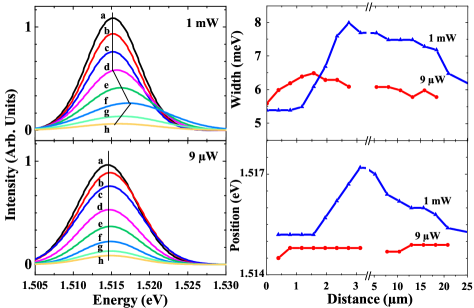
The change of width and peak position of line M is not correlated with the modification of the temperature of the Fermi sea, shown in Fig. 3, since is maximum at and constantly decreases up to 25 m. These effects cannot be attributed to a change in lattice temperature which would, at variance with observations, change the energy of other lines such as the acceptor-related lines. Finally, these changes cannot be correlated with changes of the Fermi level since, in the spatial range up to 2.5 m in which line S is observed, the width and position of this line are independent on space, implying that both the electronic quasi Fermi level and the hole level given by Eq. (2) weakly depend on space.
These considerations allow us to exclude a modification of the Fermi sea as an explanation of the results of Fig. 8. We rather believe that the change is caused by the modification of the photohole occupation probability of the valence band tail. Calculations using Eq. (3) and model parameters have indeed predicted, as observed here, that the line peak shifts to high energy upon increase of the photocarrier concentration Levanyuk and Osipov (1981).
V Conclusion
We have investigated the spatial dependence of the luminescence intensity and difference spectra as a function of distance to the excitation spot in HVPE-grown, plasma-passivated GaAs NWs, at 6K and as a function of excitation power. These NWs have a n-type doping level in the low cm-3 range, implying that significant tails are present both for the conduction and the valence band. The nearbandgap luminescence line is decomposed into three components : i) a relatively broad band at an energy slightly smaller than the bandgap, caused by recombination of photoholes with intrinsic, spin-unpolarized photoelectrons; ii) at nearbandgap energy, emission caused by recombination of the spin-polarized photoelectrons with the photoholes iii) emission caused by recombination of hot spin-polarized electrons with the same photoholes.
From the compared evolution of the two types of lines as a function of distance to the excitation spot, it is possible to follow the establishment of equilibrium between the photoelectron, intrinsic electron and photohole reservoirs. It is found that, after a distance from the excitation spot of the order of 2 m, photoelectron charges are in equilibrium with intrinsic electrons. Upon increase of the excitation power, the dynamics for establishment of equilibrium becomes slower, especially near the excitation spot. In this case, modification of the hole energy distribution in the valence bandtail induces a broadening and a shift to high energy of the main luminescence emission (line M). This perturbation is visible after a characteristic distance of 1.5 m, up to about 3 m from the excitation spot and progressively returns to normal.
Finally, it is found that the photoelectron spins are not affected by the above establishement of equilibrium and that photoelectrons and the Fermi sea remain distinct spin reservoirs, although their charges are in thermodynamic equilibrium. At large excitation power, the photoelectron spin polarization is preserved up to a record distance of 20 m. The decrease of excitation power leads to an increase of the polarization losses. These losses are attributed to hopping relaxation. Achievement of spin transport over this record length implies that such NWs are good candidates for spintronics applications.
Acknowledgements.
This work was supported by Région Auvergne Rhône-Alpes (Pack ambition recherche; Convention 17 011236 01- 61617, CPERMMASYF and LabExIMobS3 (ANR-10-LABX-16-01). It was also funded by the program Investissements d ’avenir of the French ANR agency, by the French governement IDEX-SITE initiative 16-IDEX-0001 (CAP20-25), the European Commission (Auvergne FEDER Funds).References
- Krogstrup et al. (2013) P. Krogstrup, H. I. Jorgensen, M. heiss, O. Demichel, J. V. Holm, M. Aagesen, J. Nygard, and A. F. i Morral, Nature Photonics 7, 306 (2013).
- Duan et al. (2003) X. Duan, Y. Huang, R. Agarwal, and C. M. Lieber, Nature 421, 241 (2003).
- van den Berg et al. (2013) J. W. G. van den Berg, S. Nadj-Perge, V. S. Pribiag, S. R. Plissard, E. P. A. M. Bakkers, S. M. Frolov, , and L. P. Kouwenhoven, Phys. Rev. Lett. 110, 066806 (2013).
- Gabriel et al. (2013) M. N. Gabriel, J. R. Kirschbrown, J. C. Christesen, C. W. Pinion, D. F. Zigler, E. M. Grumstrup, B. P. Mehl, E. E. M. Cating, J. F. Cahoon, and J. M. Papanikolas, Nano Letters 13, 1336 (2013).
- Nagamune et al. (1995) Y. Nagamune, H. Watabe, F. Sogawa, and Y. Arakawa, Appl. Phys. Lett. 67, 1535 (1995).
- Bolinsson et al. (2011) J. Bolinsson, K. Mergenthaler, L. Samuelson, and A. Gustafsson, Journal of Crystal Growth 215, 138 (2011).
- Darbandi and Watkins (2016) A. Darbandi and S. P. Watkins, J. Appl. Phys. 120, 014301 (2016).
- Gustafsson et al. (2010) A. Gustafsson, J. Bolinsson, N. Sköld, and L. Samuelson, Appl. Phys. Lett. 97, 072114 (2010).
- Spirkoska et al. (2009) D. Spirkoska, J. Arbiol, A. Gustafsson, S. Conesa-Boj, F. Glas, I. Zardo, M. Heigoldt, M. H. Gass, A. L. Bleloch, S. Estrade, et al., Phys. Rev. B 80, 245325 (2009).
- Gutsche et al. (2012) C. Gutsche, R. Niepelt, M. Gnauck, A. Lysov, W. Prost, C. Ronning, and F. Tegude, Nano Letters 12, 1453 (2012).
- Dzhioev et al. (2002) R. I. Dzhioev, K. V. Kavokin, V. L. Korenev, M. V. Lazarev, B. Y. Meltser, M. N. Stepanova, B. P. Zakharchenya, D. Gammon, and D. S. Katzer, Phys. Rev. B 66, 245204 (2002).
- Romer et al. (2010) M. Romer, H. Bernien, G. Muller, D. Schuh, J. Hubner, and M. Oestreich, Phys. Rev. B 81, 075216 (2010).
- D’yakonov and Perel (1971) M. I. D’yakonov and V. I. Perel, JETP Lett. 13, 467 (1971).
- Efros et al. (1972) A. L. Efros, Y. S. Halpern, and B. I. Shklovsky, Proceedings of the International Conference on Physics of semiconductors, Warsaw 1972 (Polish Scientific publishers, Warsaw, 1972).
- Shklovskii and Efros (1984) B. I. Shklovskii and A. L. Efros, Electronic Properties of Doped Semiconductors (Springer-Verlag, Berlin, 1984).
- Borghs et al. (1989) G. Borghs, K. Bhattacharyya, K. Deneffe, P. Vanmieghem, and R. Mertens, J. Appl. Phys. 66, 4381 (1989).
- Echverria-Arondo and Sherman (2012) C. Echeverria-Arrondo and E. Y. Sherman, Phys. Rev. B 85, 085430 (2012).
- Ramdani et al. (2010) M. R. Ramdani, E. Gil, C. Leroux, Y. Andre, A. Trassoudaine, D. Castelluci, L. Bideux, G. Monier, C. Robert-Goumet, and R. Kupka, Nano Letters 10, 1836 (2010).
- Gil et al. (2014) E. Gil, V. G. Dubrovskii, G. Avit, Y. Andre, C. Leroux, K. Lekhal, J. Grecenkov, A. Trassoudaine, D. Castelluci, G. Monier, et al., Nano Letters 14, 3938 (2014).
- Hijazi et al. (2019) H. Hijazi, G. Monier, E. Gil, A. Trassoudaine, C. Bougerol, C. Leroux, D. Castelluci, C. Robert-Goumet, P. Hoggan, Y. Andre, et al., Nano Letters 19, 4498 (2019).
- Cadiz et al. (2014) F. Cadiz, P. Barate, D. Paget, D. Grebenkov, J. P. Korb, A. C. H. Rowe, T. Amand, S. Arscott, and E. Peytavit, J. Appl. Phys. 116, 023711 (2014).
- Redfield et al. (1970) D. Redfield, J. P. Wittke, and J. I. Pankove, Phys. Rev. B 2, 1830 (1970).
- Knox et al. (1988) W. H. Knox, D. S. Chemla, G. Livescu, J. E. Cunningham, and J. E. Henry, Phys. Rev. Lett. 61, 1290 (1988).
- Brill and Heiblum (1994) B. Brill and M. Heiblum, Phys. Rev. B 49, 14762 (1994).
- Benzaquen et al. (1987) M. Benzaquen, D. Walsh, and K. Mazuruk, Phys. Rev. B 36, 4748 (1987).
- Cutler and Mott (1969) M. Cutler and N. F. Mott, Phys. Rev. 181, 1336 (1969).
- Anderson (1958) P. W. Anderson, Phys. Rev. 1492, 1336 (1958).
- Goktas et al. (2018) N. I. Goktas, E. M. Fiordaliso, and R. R. LaPierre, Nanotechnol. 29, 234001 (2018).
- Mehdi et al. (2018) H. Mehdi, G. Monier, P. E. Hoggan, L. Bideux, C. Robert-Goumet, and V. G. Dubrovskii, Applied Surf. Sci. 427, 662 (2018).
- Mehdi et al. (2019) H. Mehdi, F. Réveret, C. Bougerol, C. Robert-Goumet, P. E. Hoggan, L. Bideux, B. Gruzza, J. Leymarie, and G. Monier, Appl. Surf. Sci. 495, 143586 (2019).
- André et al. (2020) Y. André, N. I. Goktas, G. Monier, H. Mehdi, C. Bougerol, L. Bideux, A. Trassoudaine, D. Paget, J. Leymarie, E. Gil, et al., Nanoexpress 1, 020019 (2020).
- De-Sheng et al. (1982) J. De-Sheng, Y. Makita, K. Ploog, and H. J. Queisser, J. Appl. Phys. 53, 999 (1982).
- Lanyon and Tuft (1979) H. P. D. Lanyon and R. A. Tuft, IEEE trans. electron devices 26, 1014 (1979).
- not (a) Since the effective diameter of the NW bulk, after removal of the surface depletion, is about 4 times the Bohr radius , screening is rather three-dimensional. However, the TF model is only indicative since it assumes that screening only induces an energy shift of the electronic states. This approximation does not hold here since localized states can be suppressed or added by the mobile carriers. As a result, a numerical self-consistent approach is necessary in order to correctly describe the screening of the fluctuations by mobile carriers.
- Lowney (1986) J. R. Lowney, J. Appl. Phys. 60, 2854 (1986).
- Levanyuk and Osipov (1981) A. P. Levanyuk and V. V. Osipov, Sov. Phys. Uspekhi 24, 187 (1981).
- Arnaudov et al. (1977) B. G. Arnaudov, V. A. Vil’kotskii, D. S. Domanevskii, S. K. Evtimova, and V. D. Tkachev, Sov. Phys. Semicond. 11, 1054 (1977).
- Chébira et al. (1992) A. Chébira, J. Chesnoy, and G. M. Gale, Phys. Rev. B 46, 4559 (1992).
- Bimberg et al. (1985) D. Bimberg, H. Munzel, A. Steckenborn, and J. Christen, Phys. Rev. B 31, 7788 (1985).
- Lee et al. (1996) N. Y. Lee, J. E. Kim, H. Y. park, D. H. Kwak, H. C. Leeb, and H. Lime, Solid State Commun. 99, 571 (1996).
- Shah et al. (1977) J. Shah, R. F. Leheny, and W. Wiegmann, Phys. Rev. B 16, 1577 (1977).
- Shahmohammadi et al. (2014) M. Shahmohammadi, G. Jacopin, J. Levrat, E. Feltin, J. F. Carlin, J. D. Ganiere, R. Butte, N. Grandjean, and B. Deveaud, Nature Comm. 5, 5251 (2014).
- not (b) Since the NW diameter is smaller than both the excitation spot and the light absorption depth, this excitation power is equivalent to a very small effective power density of cm2.
- Kisker et al. (1983) D. W. Kisker, H. Tews, and W. Rehm, J. Appl. Phys. 54, 1332 (1983).
- Skromme and Stillman (1984) B. J. Skromme and G. E. Stillman, Nature 29, 1982 (1984).
- Leymarie (1989) J. Leymarie, Thesis (Universite de Nice, Nice, 1989).
- Ruhstorfer et al. (2020) D. Ruhstorfer, S. Mejia, M. Ramsteiner, M. Doblinger, H. Riedl, J. Finley, and G. Koblmuller, Appl. Phys. Lett. 116, 052101 (2020).
- not (c) The downward shift of the conduction band minimum is probably comparable with the Fermi energy, so that the Fermi level should lie near the unperturbed conduction band minimum.
- Ulbrich et al. (1989) R. G. Ulbrich, J. A. Kash, and J. C. Tsang, Phys. Rev. Lett. 62, 949 (1989).
- Weisbuch (1977) C. Weisbuch, Nuovo Cimento 39B, 660 (1977).
- Kash et al. (1985) J. A. Kash, J. C. Tsang, and J. M. Hvam, Phys. Rev. Lett. 54, 2151 (1985).
- Seymour and Alfano (1980) R. J. Seymour and R. R. Alfano, Appl. Phys. Lett 37, 231 (1980).
- Binder et al. (1992) R. Binder, D. Scott, A. E. Paul, M. Lindberg, K. Henneberger, and S. W. Koch, Phys. Rev. B 45, 1107 (1992).
- Fatti et al. (1999) N. DelFatti, P. Langot, R. Tommasi, and F. Vallée, Phys. Rev. B 59, 4576 (1999).
- Cadiz et al. (2015) F. Cadiz, D. Paget, A. C. H. Rowe, T. Amand, P. Barate, and S. Arscott, Phys. Rev. B 91, 165203 (2015).
- Bir et al. (1975) G. L. Bir, A. G. Aronov, and G. E. Pikus, JETP 42, 705 (1975).
- Shklovskii (2006) B. I. Shklovskii, Phys. Rev. B 73, 193201 (2006).