Tunable Electronic Properties and Large Rashba Splittings Found in Few-Layer Bi2Se3/PtSe2 Van der Waals Heterostructures
Abstract
We use first-principles calculations to show that van der Waals (vdW) heterostructures consisting of few-layer Bi2Se3 and PtSe2 exhibit electronic and spintronics properties that can be tuned by varying the constituent layers. Type-II band alignment with layer-tunable band gaps and type-III band alignment with spin-splittings have been found. Most noticeably, we reveal the coexistence of Rashba-type spin-splittings (with large parameters) in both the conduction and valence band stemming from few-layer Bi2Se3 and PtSe2, respectively, which has been confirmed by spin-texture plots. We discuss the role of inversion symmetry breaking, changes in orbital hybridization and spin-orbit coupling in altering electronic dispersion near the Fermi level. Since low-temperature growth mechanisms are available for both materials, we believe that few-layer Bi2Se3/PtSe2 vdW heterostructures are feasible to realize experimentally, offering great potential for electronic and spintronics applications.
keywords:
platinum diselenide, bismuth selenide, heterostructure, Rashba, band alignments, spin-textures+46 (0)920 491930
1 Introduction
The rise of graphene undoubtedly served as a paradigm shift towards two-dimensional (2D) materials providing a versatile platform for future technological revolution 1, 2, 3. Layer-by-layer assembly of transition metal dichalcogenides (TMDCs) soon after also enabled intelligent design possibilities for van der Waals (vdW) heterostructures of all dimensions revealing numerous exotic phenomena 4, 5, 6, 7, 8, 9.
Amongst a plethora of known 2D systems, few-layer PtSe2 recently created substantial scientific interest due to the report of a range of properties, such as a layer-dependent band gap 10, high room-temperature electron mobility 11, large stretchability 12, which could be used in countless applications demonstrated for photocatalysis 13 and optoelectronics 14. Different growth mechanisms have been adopted for high-quality PtSe2 synthesis on various substrates including Pt(111) 15, silicon 16, sapphire 17 and bilayer graphene/6H-SiC (0001) 18 to list a few. Recently, complementary metal-oxide-semiconductor compatible large-scale fabrication of a trilayer PtSe2 MOSFET has been demonstrated with a current ON/OFF ratio approaching 1600 at 80 K hinting at improvements in 2D nanoelectronics 19. Moreover, monolayer PtSe2 has been shown to host helical spin-texture and show local dipole induced Rashba effect with spin-layer locking which is advantageous for electrically controllable spintronics devices 20. Heterostructures consisting of vertically stacked PtSe2/MoSe2 show type II band alignment and interface states originating from the strong-weak interlayer coupling of the constituent systems 21.
Three-dimensional (3D) topological insulator Bi2Se3 is also a promising material for spintronic applications owing to room-temperature spin-polarized surface currents 22, 23, efficient charge-to-spin conversion via doping 24, giant spin pumping and inverse spin Hall effects through ferromagnetic contacts 25. Moreover, few-layer Bi2Se3 has been shown to demonstrate interesting properties, e.g., thickness-modulated semiconducting behavior 26 in comparison to its topologically insulating (TI) bulk counterpart 27, 28. Several novel functionalities have been enabled using few-layer Bi2Se3 (e.g., coexistence of topological order and superconductivity 29, hedgehog spin texture and Berry phase tuning 30, thermoelectrics 31, and ultrafast carrier dynamics, 32). Furthermore, few-layer Bi2Se3 also shows sizable Rashba-type spin-splittings due to substrate-induced structural inversion asymmetry 26, 33, 34, 35.
As both few-layer Bi2Se3 and PtSe2 demonstrate layer-dependent properties and have several distinctive features, it is therefore of great interest to theoretically study their vdW heterostructures (by varying the number of constituent layers) and search for possible synergy effects that could be utilized. Interestingly, both materials have low temperature growth mechanisms (up to 450 °C), thus, it is likely that such heterostructures can be accomplished experimentally. Motivated by this, we employ first-principles calculations and unfold tunable and sizeable type-II and type-III band alignments as well as several different spintronics features of few-layer Bi2Se3/PtSe2 vdW heterostructures. We reveal the coexistence of Rashba-type spin-splittings in the conduction(valence) band originating from few-layer Bi2Se3(PtSe2) due to inversion symmetry breaking and structural asymmetry. Our findings provide a promising pathway to manipulate the charge and spin degrees of freedom using carefully designed vdW heterostructures for the next-generation nanoscale electronic and spintronics devices.
2 Computational method
We have performed density functional theory (DFT) calculations using the projector augmented wave method 36, 37 as implemented in the Vienna Ab-initio Simulation Package 38. For the exchange-correlation potential, we have used the non-local optB86b-vdW density functional 39, 40 to account for the van der Waals interactions between the layers as successfully employed before for similar systems 41, 42. The plane-wave cutoff energy was set to a sufficiently large value of 420 eV. A gamma-centered Monkhorst-Pack k-mesh was used for the structural relaxation whereas for the band structure calculations, the Brillouin zone integration was performed using a dense k-mesh. Moreover, to compute 2D spin-textures, we set up a 2D k-mesh () centered at the gamma-point (). For the iterative solution of the Kohn-Sham equations, we ensured the total energy to converge until the change is below eV and residual forces on the atoms to decline to less than eV/Å. Since our systems contain heavy elements, the effects of spin-orbit coupling (SOC) were taken into account in the band structure and density of states (DOS) calculations. The heterostructures were modeled using a 15 Å thick vacuum layer in the out-of-plane direction to avoid periodic images interactions. Finally, the PyProcar python library 43 and Matplotlib graphics package 44 were used for pre- and post-processing of the data and plotting.
3 Results and Discussion
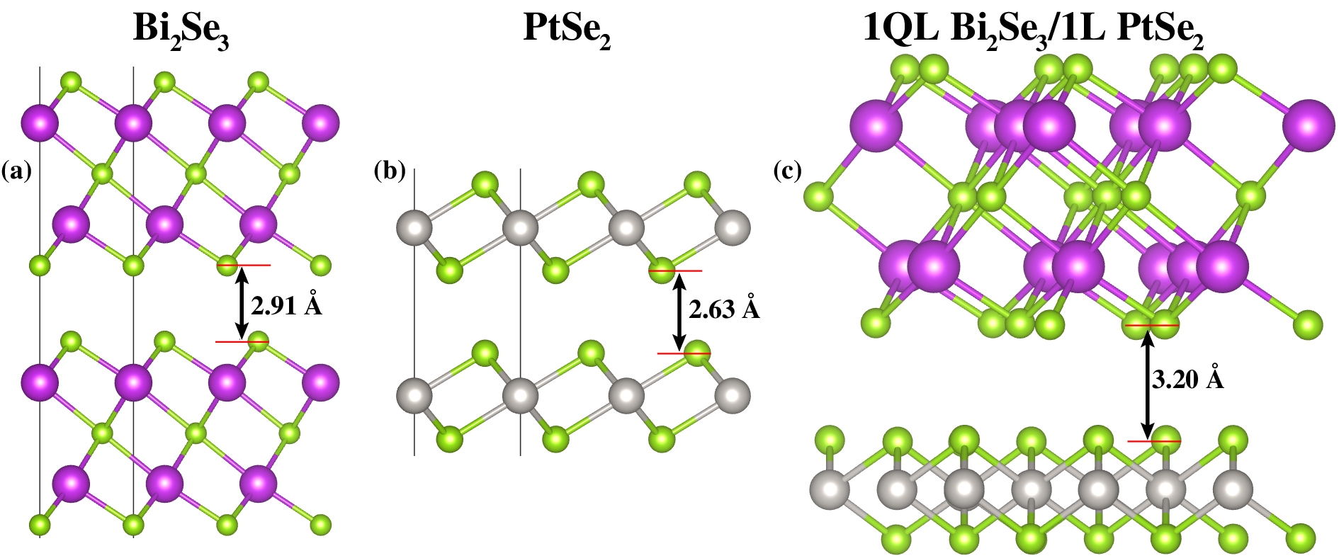
We have used DFT to simulate single- and few-layer Bi2Se3 and PtSe2 and their heterostructures, as shown in Figure 1(a-c). Each Bi2Se3 slab consists of five atomic sheets (termed a quintuple layer (QL)) having Se-Bi-Se-Bi-Se atoms held together by covalent bonding, whereas a Pt-atom is covalently sandwiched between two Se-atom-layers in a PtSe2 slab with 1T-phase trigonal geometry. The optimized lattice parameters for 1QL(2QL) Bi2Se3 and 1L(2L) PtSe2 are 4.15 Å (4.14 Å) and 3.71 Å (3.74 Å ), respectively, in close agreement with reported values. Few-layer Bi2Se3 is separated by 2.91 Å whereas Pt chalcogenides are known to experience strong interlayer interactions as evident from an interlayer distance of 2.63 Å. In order to achieve minimal lattice mismatch in forming vdW heterostructures, a supercell of Bi2Se3 is matched to a supercell of PtSe2 with a lattice parameter of 11.05 Å for the combined supercell resulting in less than 1% lattice mismatch. Similarly for other heterostructures, average lattice parameters are adopted for vdW heterostructures in subsequent calculations. Owing to the incommensurate nature of the 2D materials involved in our study, a Moiré superlattice of periodicity 1.1 nm is therefore expected to be obtained in experiments, similar to the case of PtSe2/MoSe2 heterostructures 21. The lowest-energy structure for a representative 1QL Bi2Se3/1L PtSe2 heteroestructure is given in Figure 1(c), for which different lateral stackings were carefully inspected before arriving at this configuration. We note that interlayer interactions between PtSe2 and Bi2Se3 are homogeneous meaning Bi or Se atoms do not prefer particular sites on PtSe2. For six different lateral stacking configurations, shown in supplementary Figure LABEL:fig:figs1(a-f), the energy differences fall in the of range 0 to 10 meV from which the minimum energy configuration is adopted for calculations.
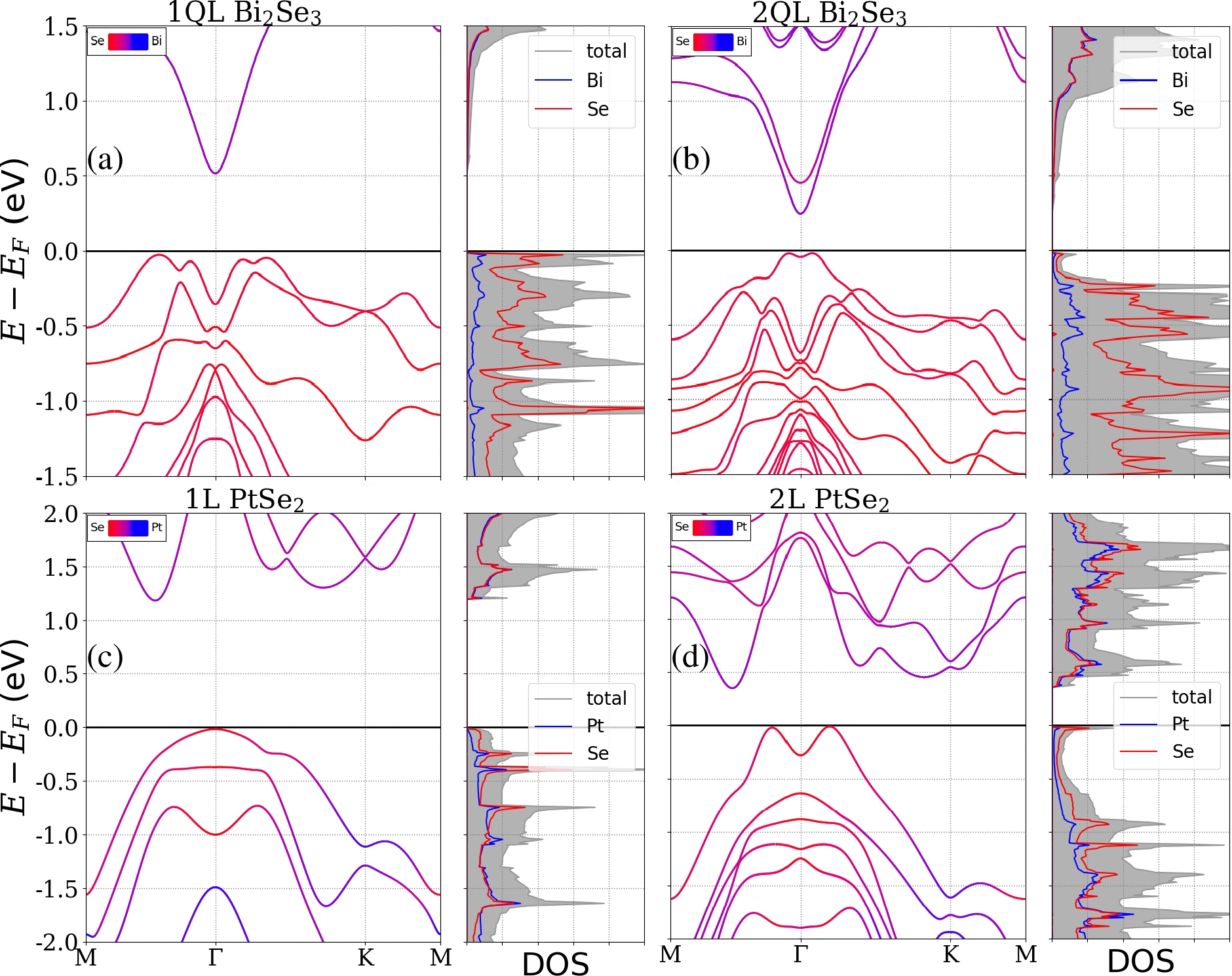
We first determine the electronic properties of pristine few-layer Bi2Se3 and PtSe2 (see Figure 2). A layer-dependent band gap with decreasing magnitude is observed in both cases. For 1QL(2QL) Bi2Se3, incorporating the effect of SOC, an indirect band gap of 0.55 eV(0.26 eV) is observed as shown in Figure 2(a,b), respectively. The conduction band (CB) minimum for 1QL is located at the high-symmetry -point whereas the valence band (VB) maximum lies along the -M direction. Looking at the atom projected DOS (PDOS), the VB consists mainly of Se) states and small contribution from Bi states whereas the CB contains evenly mixed Se-Bi states. For 1L(2L) PtSe2, we observe a comparatively larger indirect band gap of 1.20 eV(0.36 eV) with the CB minimum lying along the -M direction and the VB maximum is located at the high-symmetry -point for 1L (see Figure 2(c,d)). For 1L PtSe2, the VB comprises also of Se) states and minuscule Pt contribution present near the Fermi level that gradually escalates in magnitude in moving away from it. The CB of few-layer PtSe2 however also involves equally mixed Se-Pt states much alike few-layer Bi2Se3. The reason for the differences between 1(Q)L and 2(Q)L is that although the strong interlayer binding is of van der Waals type, the resulting physisorption leads to induced moments and Pauli repulsion of the electron density (contracted in the layers) that effects the properties since the layers are squeezed together compared to a monolayer 45. Unlike other TMDCs such as MoS2, layer-tunable band gaps and mixed atomic hybridization in both few-layer Bi2Se3 and PtSe2 influences the observed novel features described above, as will be discussed in the following section.
We have considered four different heterostructures combining few-layer Bi2Se3 and PtSe2, denoted nQL Bi2Se3/nL PtSe2 (see Table 1), for which we report the structural and energetic properties. The binding energy per PtSe2 is calculated through equation (1),
| (1) |
where is the total energy of the few-layer vdW heterostructure, is the total energy of detached nQL Bi2Se3, and is the total energy of detached nL PtSe2 considered in the heterostructures, where n. We have found the layers of Bi2Se3 and PtSe2 to bind through physisorption, as expected, and these are thus vdW heterostructures.
| Heterostructure | BAlignment | ||||
|---|---|---|---|---|---|
| 1QL Bi2Se3/1L PtSe2 | 11.05 | 3.20 | -0.63 | 100 | Type-II |
| 2QL Bi2Se3/1L PtSe2 | 11.04 | 3.17 | -0.63 | 50 | Type-II |
| 1QL Bi2Se3/2L PtSe2 | 11.10 | 3.12 | -0.66 | Type-III | |
| 2QL Bi2Se3/2L PtSe2 | 11.08 | 3.12 | -0.66 | Type-III |
Looking at the binding energy (), it is clear that 1L PtSe2 binds much stronger to 1QL Bi2Se3 (-0.63 eV/PtSe2) in comparison to the recently studied case of 1L MoSe2/1L PtSe2 (-0.25 eV/PtSe2) 21. Moreover, we observe that increasing the PtSe2 thickness further enhances the interlayer coupling as increases to -0.66 eV/PtSe2 in moving from 1L to 2L PtSe2. The contraction in interlayer distance (3.20 Å to 3.12 Å) also validate this argument. On the other hand, adding a second QL of Bi2Se3 to the heterostructure shows negligible change in both binding energy and interlayer distance. It is worth mentioning that the interlayer distance in vdW heterostructures is always longer than pristine few-layer Bi2Se3 and PtSe2 showing relatively weaker interaction than for the constituent systems.
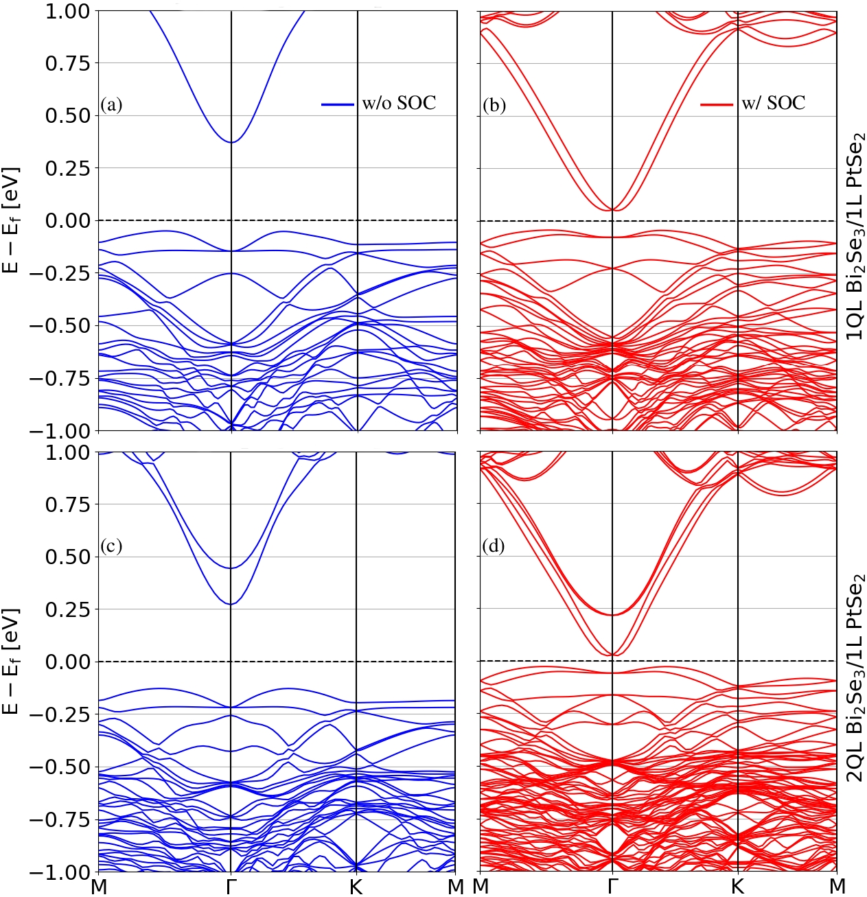
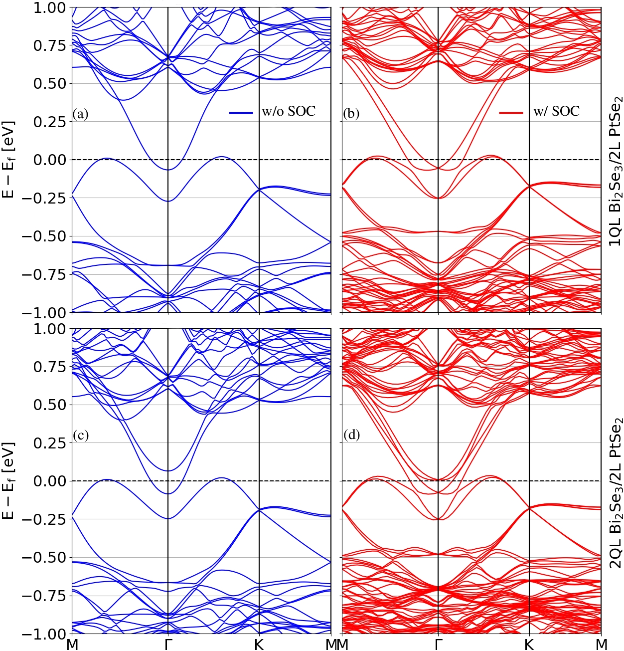
For the 1QL(2QL) Bi2Se3/1L PtSe2 heterostructure, including the effect of SOC (see Figure 3(b,d)), we found a type-II band alignment with layer-tunable indirect band gaps of 100 meV(50 meV), respectively. The CB minimum is present at the high symmetry -point coming from few-layer Bi2Se3 and the VB is contributed by 1L PtSe2 having its maximum along the -M direction (see supplementary Figure LABEL:fig:figs2(a)). Comparing to the case without SOC (Figure 3(a,c)), the SOC significantly affects the magnitude of the band gaps in the vdW heterostructures much alike pristine 1QL(2QL) Bi2Se3 (see supplementary Figure LABEL:fig:figs3(a-d)). For the 1QL(2QL) Bi2Se3/1L PtSe2 heterostructures the energy gap shrinks with the type-II band alignment when going from 1QL to 2QL, which is in line with the change of the CB in pristine Bi2Se3 in 1QL and 2QL (c.f. Figure 2(a,b)). In the context of theoretical predictions of strongly bound excitons in 1L PtSe2 46 and the recent experimental observation of chiral surface excitons in a TI Bi2Se3 47, our findings are highly intriguing because they hint at possible control of low-energy interlayer excitons by forming layer-controlled vdW heterostructures. Moreover, following the trend of the band gap values, it is anticipated that the band gap will eventually vanish at around 4QLs Bi2Se3/1L PtSe2 vdW heterostructure.
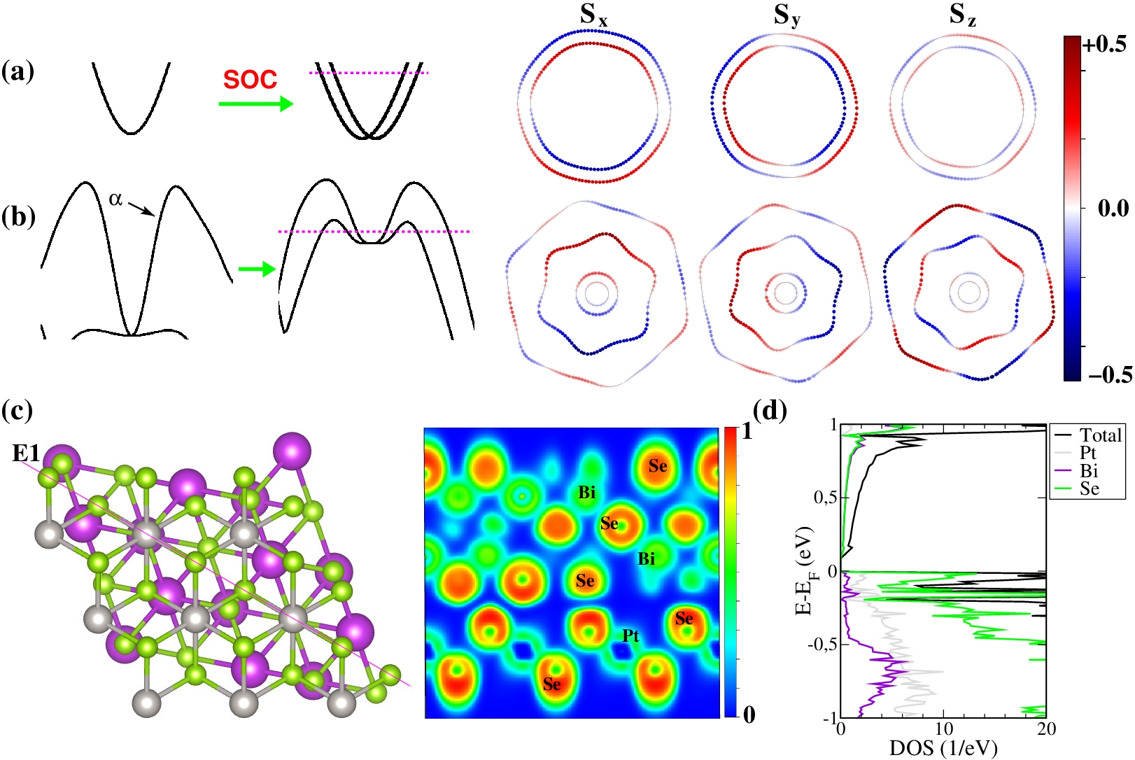
Interestingly, besides layer-tunable type-II band alignment, we also observe coexistence of Rashba-type spin-splittings (in the CB) and hedgehog-like band-splittings (in the VB) of 1QL(2QL) Bi2Se3/1L PtSe2 vdW heterostructures. The crystal structures of few-layer Bi2Se3 have inversion symmetry (i.e., ) which does not remain intact for vdW heterostructures with 1L PtSe2. Applying SOC therefore lifts the spin-degeneracy and display Rashba-type spin-splittings in the CB originating from few-layer Bi2Se3. We note that these splittings resemble to those observed in graphene/TI vdW heterostructures resulting in gate-tunable spin-galvanic effects at room temperature 48. To confirm this, we set up a -centered 2D k-mesh along the xy-plane and plot the fixed-energy contours of spin components , and as shown in Figure 4(a) alongside the transformation of the CB with respect to the SOC effect. The typical Rashba-split bands along the momentum-axis with large(small) in-plane(out-of-plane) spin components, respectively, support our findings. Using the Rashba Hamiltonian for 2D-electron gas,
| (2) |
where and being the in-plane momentum and effective mass of electron, is the Rashba parameter, is the vector of Pauli matrices and is the out-of-plane unit vector. Taking as the energy difference between the CB minimum and band crossing at the -point and as the momentum offset, the Rashba parameter for a parabolic-dispersion is approximated by , whereas and . For 1QL(2QL) Bi2Se3/1L PtSe2 vdW heterostructures, we obtain and thus giving , respectively. These values for the Rashba parameter () are amongst the highest found, compared to similar 2D vdW heterostructures (see supplementary Table LABEL:table:tables1). Moreover, a slight decrease in moving from 1QL to 2QL Bi2Se3 suggests layer-tunable spintronics in these vdW heterostructures. Furthermore, another striking feature is the presence of a giant energy interval of 0.9 eV above the Fermi level and inside the band gap of 1L PtSe2 without any non-Rashba states. This constitutes a complete 2D Rashba electron-gas in 1QL Bi2Se3/1L PtSe2 vdW heterostructure further extending the limit from Ref. 35. Having consistent behavior for 2QL Bi2Se3/1L PtSe2 with lesser magnitude (0.2 eV) of pure Rashba-split CB, our results point towards a promising route to design Datta Das spin field-effect transistor out of these few-layer vdW heterostructures.
On the other end, looking at the topmost VB of the band structure coming from 1L PtSe2, it is seen turning into a “Mexican hat” shape (compare Figure 3(a,c) to supplementary Figure LABEL:fig:figs4(c) for the band structure of pristine 1L PtSe2). The upper VB of 1L PtSe2 (called -band, see Figure 4(b)) is mainly formed from the in-plane -orbitals of Se atoms. We have analyzed the interlayer interaction using the electron localization function (EFL), as can be seen in Figure 4(c), and find Bi2Se3 to be bound with PtSe2 by vdW physisorption. The electron density of a 1QL(2QL) Bi2Se3/1L PtSe2 shrinks compared to a single layer due to the induced moments and Pauli repulsion as mentioned above and shown for graphene/graphite in Ref. 45. This contraction can be seen comparing the interface with the outer surfaces of Bi2Se3 and PtSe2 in Figure 4(c), and leads to perturbations of the chemical bonds within the layers and results in changes to the band structure as seen in Figure 4(b). Moreover, the total and atom projected DOS shown in Figure 4(d) confirm the changes in orbital hybridization between Se- and Bi/Pt-states near the Fermi level compared to Figure 2. Moreover, orbital-projected band structures of 1QL Bi2Se3/1L PtSe2 vdW heterostructure, given in the supplementary Figure LABEL:fig:figs2prime(a,b), show much larger Se-orbital hybridization in the VB compared to the CB. In the 1T-phase, 1L PtSe2 holds centrosymmetry with D3d point group which does not remain intact due to the different charge environment experienced by the top and bottom Se-layers. Applying SOC therefore lifts the spin-degeneracy and produce hedgehog-like band-splittings without any net spin polarization for which the underlying theoretical formalism is discussed in Ref. 49 and resembles that of the recently realized experiment of Ref. 50. To make this point clear, we show the transformation of the VB due to SOC along fixed-energy contours of the spin components , and in Figure 4(b). One may also distinguish between Rashba-type spin-splittings of the CB and hedgehog-like band-splittings of the VB by looking at the fixed-energy contours of the spin-components in both Figure 4(a) and 4(b) right-side, respectively.
We also considered the effect of increasing the PtSe2 thickness, i.e., few-layer Bi2Se3/2L PtSe2, for which the band structures show type-III band alignment as displayed in Figure 5(a-d) and supplementary Figure LABEL:fig:figs2(b). Interestingly, both the CB and VB simultaneously show Rashba-type spin-splittings with each band being located on the separate constituent materials. The broken inversion symmetry is valid as for 1QL(2QL) Bi2Se3/2L PtSe2 (i.e., top and bottom constituent layers experience different charge environment). Approximating the band dispersion around the -point by Eq. 2, Table 2 lists the corresponding parameters for all vdW heterostructures considered in this study. Most notably, at a momentum offset Å-1 and giant Rashba spin-splitting energy of meV, the resultant eV Å for few-layer Bi2Se3/2L PtSe2 are amongst the highest values reported to date (see supplementary Table LABEL:table:tables1). Moreover, the values for the CB also show the formation of a Rashba electron-gas over a large energy interval.
| Heterostructure | |||
|---|---|---|---|
| 1QL Bi2Se3/1L PtSe2 | 4.8 | 0.002 | 4.80 (CB) |
| 2QL Bi2Se3/1L PtSe2 | 4.0 | 0.002 | 4.00 (CB) |
| 2QL Bi2Se3/1L PtSe2 | 15 | 0.006 | 5.00 (CB) |
| 275 | 0.033 | 16.66 (VB) | |
| 2QL Bi2Se3/2L PtSe2 | 11 | 0.005 | 4.40 (CB) |
| 278 | 0.033 | 16.84 (VB) |
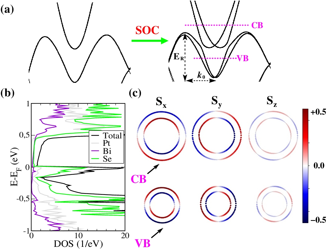
To better describe these Rashba spin-splittings and associated spin-textures, Figure 6(a) shows the bands changeover under the influence of SOC alongside the definition of and for the VB. Also, the total and atom projected DOS in Figure 6(b) display significant changes in the orbital hybridization within the Bi2Se3 and PtSe2 layers around the Fermi level as compared to Figure 2, which is responsible for large SOC induced spin-splittings. We clarify this by plotting atomic-projected band structure of 1L Bi2Se3/2L PtSe2 vdW heterostructures, shown in supplementary Figure LABEL:fig:figs2prime(c,d), where Se-atomic orbitals in the vicinity of the Fermi level hybridize and give rise to spin-splittings. In order to confirm the Rashba-shift along the momentum axis, we also give fixed-energy contour plots of spin-components , , and which corroborates our findings and reveal in-plane spin-components with minuscule out-of-plane contributions for both the CB and the VB as shown in Figure 6(c). Comparing spin-splittings and Rashba-energies in the CB and the VB, we observe energy anisotropy in the spin texture similar to the case of graphene/TI heterostructure 51. Since the optB86b-vdW functional is known to underestimate the band gap compared to experiment (and the use of a more accurate hybrid functional, such as HSE06, is prohibited due to the size of the models), it is anticipated that the transformation of type-II to type-III band alignment will occur at larger PtSe2 thickness than 2L, which makes it possible to access the novel spintronics features predicted for these vdW heterostructures with few-layer Bi2Se3. Furthermore, low-temperature synthesis techniques are available for both systems, which also favors the formation of stacked vdW heterostructures.
4 Conclusion
In summary, we employed density functional theory calculations to discuss layer-dependent electronic properties of few-layer Bi2Se3 and PtSe2 van der Waals heterostructures. By varying the constituent layers, four different vdW heterostructures were constructed for which we provided details of structural, electronic and spintronics properties. It turned out that it is possible to simultaneously achieve type-II band alignment with layer-tunable band gaps and a complete 2D Rashba electron-gas spanning over a large energy interval of 0.9 eV for few-layer Bi2Se3/1L PtSe2 vdW heterostructures. Fixed-energy contour plots of spin-components are presented to distinguish between Rashba- and hedgehog-like spin-textures of the CB and the VB originating from different constituent layers. By increasing the PtSe2 thickness from 1L to 2L, we showed that type-II band alignment can be transformed to type-III. Moreover, we also revealed the coexistence of Rashba-like spin-splittings in both the CB (originating from Bi2Se3) and the VB (coming from PtSe2) of few-layer Bi2Se3/2L PtSe2 vdW heterostructures for which the corresponding spin-textures also support our findings. The role of inversion symmetry breaking, spin-orbit coupling and changes to the atomic orbital hybridization at the interface between few-layer Bi2Se3 and PtSe2 is highlighted to understand and interpret the electronic dispersion. The electron localization function was used to analyze the interlayer binding and shows the contraction of the electron density within the Bi2Se3 and PtSe2 layers. Our findings provide a unique avenue to manipulate the charge and spin degrees of freedom by exploiting few-layer Bi2Se3/PtSe2 vdW heterostructures for potential electronic and spintronics applications.
Fruitful discussions with Muhammad Tahir and Aurélien Manchon are greatly acknowledged. We thank Knut och Alice Wallenberg foundation, Kempestiftelserna and Interreg Nord for financial support. We also thank High Performance Computing Center North (HPC2N), National Supercomputer Center in Linköping (NSC), and the PDC Center for High Performance Computing for allocation of time and resources, through the Swedish National Infrastructure for Computing (SNIC).
Competing Interests
The Authors declare no competing financial or non-financial interests.
Data Availability
The data that support the findings of this study are available from the corresponding author upon reasonable request.
Author Contribution
S. Sattar performed the calculations, J. A. Larsson analysed the results. All authors reviewed the manuscript.
References
- Novoselov et al. 2004 Novoselov, K. S.; Geim, A. K.; Morozov, S. V.; Jiang, D.; Zhang, Y.; Dubonos, S. V.; Grigorieva, I. V.; Firsov, A. A. Electric Field Effect in Atomically Thin Carbon Films. Science 2004, 306, 666–669
- Novoselov et al. 2005 Novoselov, K. S.; Geim, A. K.; Morozov, S.; Jiang, D.; Katsnelson, M. I.; Grigorieva, I.; Dubonos, S.; Firsov, A. A. Two-Dimensional Gas of Massless Dirac Fermions in Graphene. Nature 2005, 438, 197–200
- Zhang et al. 2005 Zhang, Y.; Tan, Y.-W.; Stormer, H. L.; Kim, P. Experimental Observation of the Quantum Hall Effect and Berry’s Phase in Graphene. Nature 2005, 438, 201–204
- Novoselov et al. 2005 Novoselov, K. S.; Jiang, D.; Schedin, F.; Booth, T. J.; Khotkevich, V. V.; Morozov, S. V.; Geim, A. K. Two-Dimensional Atomic Crystals. Proceedings of the National Academy of Sciences 2005, 102, 10451–10453
- Mak et al. 2010 Mak, K. F.; Lee, C.; Hone, J.; Shan, J.; Heinz, T. F. Atomically Thin : A New Direct-Gap Semiconductor. Phys. Rev. Lett. 2010, 105, 136805
- Radisavljevic et al. 2011 Radisavljevic, B.; Radenovic, A.; Brivio, J.; Giacometti, V.; Kis, A. Single-layer MoS2 Transistors. Nature Nanotechnology 2011, 6, 147
- Mas-Ballesté et al. 2011 Mas-Ballesté, R.; Gómez-Navarro, C.; Gómez-Herrero, J.; Zamora, F. 2D Materials: To Graphene and Beyond. Nanoscale 2011, 3, 20–30
- Geim and Grigorieva 2013 Geim, A. K.; Grigorieva, I. V. Van der Waals Heterostructures. Nature 2013, 499, 419–425
- Xiang et al. 2020 Xiang, R.; Inoue, T.; Zheng, Y.; Kumamoto, A.; Qian, Y.; Sato, Y.; Liu, M.; Tang, D.; Gokhale, D.; Guo, J.; Hisama, K.; Yotsumoto, S.; Ogamoto, T.; Arai, H.; Kobayashi, Y.; Zhang, H.; Hou, B.; Anisimov, A.; Maruyama, M.; Miyata, Y.; Okada, S.; Chiashi, S.; Li, Y.; Kong, J.; Kauppinen, E. I.; Ikuhara, Y.; Suenaga, K.; Maruyama, S. One-Dimensional van der Waals Heterostructures. Science 2020, 367, 537–542
- Ciarrocchi et al. 2018 Ciarrocchi, A.; Avsar, A.; Ovchinnikov, D.; Kis, A. Thickness-Modulated Metal-to-Semiconductor Transformation in a Transition Metal Dichalcogenide. Nature Communications 2018, 9, 1–6
- Zhao et al. 2017 Zhao, Y.; Qiao, J.; Yu, Z.; Yu, P.; Xu, K.; Lau, S. P.; Zhou, W.; Liu, Z.; Wang, X.; Ji, W.; Chai, Y. High-Electron-Mobility and Air-Stable 2D Layered PtSe2 FETs. Advanced Materials 2017, 29, 1604230
- Okogbue et al. 2019 Okogbue, E.; Han, S. S.; Ko, T.-J.; Chung, H.-S.; Ma, J.; Shawkat, M. S.; Kim, J. H.; Kim, J. H.; Ji, E.; Oh, K. H.; Zhai, L.; Lee, G.-H.; Jung, Y. Multifunctional Two-Dimensional PtSe2-Layer Kirigami Conductors with 2000% Stretchability and Metallic-to-Semiconducting Tunability. Nano Letters 2019, 19, 7598–7607
- Sun et al. 2020 Sun, X.; Zhang, H.; Li, X.; Zheng, Y.-Z.; Wu, J.; Li, N.; Ding, H.; Lv, X.; Tao, X. An Efficient and Extremely Stable Photocatalytic PtSe2/FTO Thin Film for Water Splitting. Energy Technology 2020, 8, 1900903
- Yim et al. 2016 Yim, C.; Lee, K.; McEvoy, N.; O’Brien, M.; Riazimehr, S.; Berner, N. C.; Cullen, C. P.; Kotakoski, J.; Meyer, J. C.; Lemme, M. C.; Duesberg, G. S. High-Performance Hybrid Electronic Devices from Layered PtSe2 Films Grown at Low Temperature. ACS Nano 2016, 10, 9550–9558
- Wang et al. 2015 Wang, Y.; Li, L.; Yao, W.; Song, S.; Sun, J. T.; Pan, J.; Ren, X.; Li, C.; Okunishi, E.; Wang, Y.-Q.; Wang, E.; Shao, Y.; Zhang, Y. Y.; Yang, H.-T.; Schwier, E. F.; Iwasawa, H.; Shimada, K.; Taniguchi, M.; Cheng, Z.; Zhou, S.; Du, S.; Pennycook, S. J.; Pantelides, S. T.; Gao, H.-J. Monolayer PtSe2, a New Semiconducting Transition-Metal-Dichalcogenide, Epitaxially Grown by Direct Selenization of Pt. Nano Letters 2015, 15, 4013–4018
- Ansari et al. 2019 Ansari, L.; Monaghan, S.; McEvoy, N.; Coileáin, C. Ó.; Cullen, C. P.; Lin, J.; Siris, R.; Stimpel-Lindner, T.; Burke, K. F.; Mirabelli, G.; Duffy, R.; Caruso, E.; Nagle, R. E.; Duesberg, G. S.; Hurley, P. K.; Gity, F. Quantum Confinement-Induced Semimetal-to-Semiconductor Evolution in Large-Area Ultra-Thin PtSe2 Films Grown at 400 °C. npj 2D Materials and Applications 2019, 3, 1–8
- Wang et al. 2016 Wang, Z.; Li, Q.; Besenbacher, F.; Dong, M. Facile Synthesis of Single Crystal PtSe2 Nanosheets for Nanoscale Electronics. Advanced Materials 2016, 28, 10224–10229
- Yan et al. 2017 Yan, M.; Wang, E.; Zhou, X.; Zhang, G.; Zhang, H.; Zhang, K.; Yao, W.; Lu, N.; Yang, S.; Wu, S.; Yoshikawa, T.; Miyamoto, K.; Okuda, T.; Wu, Y.; Yu, P.; Duan, W.; Zhou, S. High Quality Atomically Thin PtSe2 Films Grown by Molecular Beam Epitaxy. 2D Materials 2017, 4, 045015
- Xiong et al. 2020 Xiong, K.; Hilse, M.; Li, L.; Göritz, A.; Lisker, M.; Wietstruck, M.; Kaynak, M.; Engel-Herbert, R.; Madjar, A.; Hwang, J. C. M. Large-Scale Fabrication of Submicrometer-Gate-Length MOSFETs With a Trilayer PtSe2 Channel Grown by Molecular Beam Epitaxy. IEEE Transactions on Electron Devices 2020, 67, 796–801
- Yao et al. 2017 Yao, W.; Wang, E.; Huang, H.; Deng, K.; Yan, M.; Zhang, K.; Miyamoto, K.; Okuda, T.; Li, L.; Wang, Y.; Gao, H.; Liu, C.; Duan, W.; Zhou, S. Direct Observation of Spin-Layer Locking by Local Rashba Effect in Monolayer Semiconducting PtSe2 Film. Nature Communications 2017, 8, 1–6
- Zhou et al. 2019 Zhou, J.; Kong, X.; Sekhar, M. C.; Lin, J.; Le Goualher, F.; Xu, R.; Wang, X.; Chen, Y.; Zhou, Y.; Zhu, C.; Lu, W.; Liu, F.; Tang, B.; Guo, Z.; Zhu, C.; Cheng, Z.; Yu, T.; Suenaga, K.; Sun, D.; Ji, W.; Liu, Z. Epitaxial Synthesis of Monolayer PtSe2 Single Crystal on MoSe2 with Strong Interlayer Coupling. ACS Nano 2019, 13, 10929–10938
- Li et al. 2014 Li, C.; Van‘t Erve, O.; Robinson, J.; Liu, Y.; Li, L.; Jonker, B. Electrical detection of charge-current-induced spin polarization due to spin-momentum locking in Bi2Se3. Nature nanotechnology 2014, 9, 218
- Dankert et al. 2015 Dankert, A.; Geurs, J.; Kamalakar, M. V.; Charpentier, S.; Dash, S. P. Room temperature electrical detection of spin polarized currents in topological insulators. Nano letters 2015, 15, 7976–7981
- Dankert et al. 2018 Dankert, A.; Bhaskar, P.; Khokhriakov, D.; Rodrigues, I. H.; Karpiak, B.; Kamalakar, M. V.; Charpentier, S.; Garate, I.; Dash, S. P. Origin and evolution of surface spin current in topological insulators. Physical Review B 2018, 97, 125414
- 25 Giant spin pumping and inverse spin Hall effect in the presence of surface and bulk spin- orbit coupling of topological insulator Bi2Se3.
- Zhang et al. 2010 Zhang, Y.; He, K.; Chang, C.-Z.; Song, C.-L.; Wang, L.-L.; Chen, X.; Jia, J.-F.; Fang, Z.; Dai, X.; Shan, W.-Y., et al. Crossover of the Three-Dimensional Topological Insulator Bi2Se3 to the Two-Dimensional Limit. Nature Physics 2010, 6, 584–588
- Zhang et al. 2009 Zhang, H.; Liu, C.-X.; Qi, X.-L.; Dai, X.; Fang, Z.; Zhang, S.-C. Topological Insulators in Bi2Se3, Bi2Te3 and Sb2Te3 With a Single Dirac Cone on the Surface. Nature Physics 2009, 5, 438–442
- Hsieh et al. 2009 Hsieh, D.; Xia, Y.; Qian, D.; Wray, L.; Dil, J. H.; Meier, F.; Osterwalder, J.; Patthey, L.; Checkelsky, J. G.; Ong, N. P.; Fedorov, A. V.; Lin, H.; Bansil, A.; Grauer, D.; Hor, Y. S.; Cava, R. J.; Hasan, M. Z. A Tunable Topological Insulator in the Spin Helical Dirac Transport Regime. Nature 2009, 460, 1101–1105
- Wang et al. 2012 Wang, M.-X.; Liu, C.; Xu, J.-P.; Yang, F.; Miao, L.; Yao, M.-Y.; Gao, C. L.; Shen, C.; Ma, X.; Chen, X.; Xu, Z.-A.; Liu, Y.; Zhang, S.-C.; Qian, D.; Jia, J.-F.; Xue, Q.-K. The Coexistence of Superconductivity and Topological Order in the Bi2Se3 Thin Films. Science 2012, 336, 52–55
- Xu et al. 2012 Xu, S.-Y.; Neupane, M.; Liu, C.; Zhang, D.; Richardella, A.; Wray, L. A.; Alidoust, N.; Leandersson, M.; Balasubramanian, T.; Sánchez-Barriga, J.; Rader, O.; Landolt, G.; Slomski, B.; Dil, J. H.; Osterwalder, J.; Chang, T.-R.; Jeng, H.-T.; Bansil, A.; Samarth, N.; Hasan, M. Z. Hedgehog Spin Texture and Berry’s Phase Tuning in a Magnetic Topological Insulator. Nature Physics 2012, 8, 616–622
- Guo et al. 2016 Guo, M.; Wang, Z.; Xu, Y.; Huang, H.; Zang, Y.; Liu, C.; Duan, W.; Gan, Z.; Zhang, S.-C.; He, K.; Ma, X.; Xue, Q.; Wang, Y. Tuning Thermoelectricity in a Bi2Se3 Topological Insulator via Varied Film Thickness. New Journal of Physics 2016, 18, 015008
- Glinka et al. 2013 Glinka, Y. D.; Babakiray, S.; Johnson, T. A.; Bristow, A. D.; Holcomb, M. B.; Lederman, D. Ultrafast Carrier Dynamics in Thin-Films of the Topological Insulator Bi2Se3. Applied Physics Letters 2013, 103, 151903
- Benia et al. 2013 Benia, H. M.; Yaresko, A.; Schnyder, A. P.; Henk, J.; Lin, C. T.; Kern, K.; Ast, C. R. Origin of Rashba Splitting in the Quantized Subbands at the Bi2Se3 surface. Phys. Rev. B 2013, 88, 081103
- Zhang and Schwingenschlögl 2018 Zhang, Q.; Schwingenschlögl, U. Rashba Effect and Enriched Spin-Valley Coupling in / ( = Mo, W; = S, Se, Te) Heterostructures. Phys. Rev. B 2018, 97, 155415
- Wang and Jeng 2017 Wang, T.-H.; Jeng, H.-T. Wide-Range Ideal 2D Rashba Electron Gas with Large Spin Splitting in Bi2Se3/MoTe2 Heterostructure. npj Computational Materials 2017, 3, 1–6
- Blöchl 1994 Blöchl, P. E. Projector Augmented-Wave Method. Phys. Rev. B 1994, 50, 17953–17979
- Kresse and Furthmüller 1996 Kresse, G.; Furthmüller, J. Efficient Iterative Schemes for Ab Initio Total-Energy Calculations Using a Plane-Wave Basis Set. Phys. Rev. B 1996, 54, 11169–11186
- Kresse and Joubert 1999 Kresse, G.; Joubert, D. From Ultrasoft Pseudopotentials to the Projector Augmented-Wave Method. Phys. Rev. B 1999, 59, 1758–1775
- Klimeš et al. 2009 Klimeš, J.; Bowler, D. R.; Michaelides, A. Chemical Accuracy For the Van der Waals Density Functional. Journal of Physics: Condensed Matter 2009, 22, 022201
- Klimeš et al. 2011 Klimeš, J.; Bowler, D. R.; Michaelides, A. Van der Waals Density Functionals Applied to Solids. Phys. Rev. B 2011, 83, 195131
- Peng et al. 2016 Peng, Q.; Wang, Z.; Sa, B.; Wu, B.; Sun, Z. Electronic Structures and Enhanced Optical Properties of Blue Phosphorene/Transition Metal Dichalcogenides van der Waals Heterostructures. Scientific reports 2016, 6, 31994
- Sharma and Schwingenschlögl 2016 Sharma, S.; Schwingenschlögl, U. Thermoelectric Response in Single Quintuple Layer Bi2Te3. ACS Energy Letters 2016, 1, 875–879
- Herath et al. 2020 Herath, U.; Tavadze, P.; He, X.; Bousquet, E.; Singh, S.; Muñoz, F.; Romero, A. H. PyProcar: A Python Library for Electronic Structure Pre/Post-Processing. Computer Physics Communications 2020, 251, 107080
- Hunter 2007 Hunter, J. D. Matplotlib: A 2D Graphics Environment. Computing in Science Engineering 2007, 9, 90–95
- Koumpouras and Larsson 2020 Koumpouras, K.; Larsson, J. A. Distinguishing Between Chemical Bonding and Physical Binding Using Electron Localization Function (ELF). Journal of Physics: Condensed Matter 2020, 32, 315502
- Sajjad et al. 2018 Sajjad, M.; Singh, N.; Schwingenschlögl, U. Strongly Bound Excitons in Monolayer PtS2 and PtSe2. Applied Physics Letters 2018, 112, 043101
- Kung et al. 2019 Kung, H.-H.; Goyal, A. P.; Maslov, D. L.; Wang, X.; Lee, A.; Kemper, A. F.; Cheong, S.-W.; Blumberg, G. Observation of Chiral Surface Excitons in a Topological Insulator Bi2Se3. Proceedings of the National Academy of Sciences 2019, 116, 4006–4011
- Khokhriakov et al. 2020 Khokhriakov, D.; Hoque, A. M.; Karpiak, B.; Dash, S. P. Gate-tunable spin-galvanic effect in graphene-topological insulator van der Waals heterostructures at room temperature. Nature communications 2020, 11, 1–7
- Liu et al. 2019 Liu, K.; Luo, W.; Ji, J.; Barone, P.; Picozzi, S.; Xiang, H. Band Splitting with Vanishing Spin Polarizations in Noncentrosymmetric Crystals. Nature Communications 2019, 10, 1–6
- Sakano et al. 2020 Sakano, M.; Hirayama, M.; Takahashi, T.; Akebi, S.; Nakayama, M.; Kuroda, K.; Taguchi, K.; Yoshikawa, T.; Miyamoto, K.; Okuda, T.; Ono, K.; Kumigashira, H.; Ideue, T.; Iwasa, Y.; Mitsuishi, N.; Ishizaka, K.; Shin, S.; Miyake, T.; Murakami, S.; Sasagawa, T.; Kondo, T. Radial Spin Texture in Elemental Tellurium with Chiral Crystal Structure. Phys. Rev. Lett. 2020, 124, 136404
- Khokhriakov et al. 2018 Khokhriakov, D.; Cummings, A. W.; Song, K.; Vila, M.; Karpiak, B.; Dankert, A.; Roche, S.; Dash, S. P. Tailoring emergent spin phenomena in Dirac material heterostructures. Science Advances 2018, 4, eaat9349
The Supporting Information contains (1) Different lateral stacking configurations of Bi2Se3/PtSe2 vdW heterostructure considered to obtain minimum-energy configuration. (2) Layer-projected band structure of Bi2Se3/PtSe2 vdW heterostructures to show type-II and type-III band alignments. (3) Band structures of few-layer Bi2Se3. (4) Band structures of supercells of Bi2Se3 and PtSe2. (5) Atomic orbital-projected band structures of Bi2Se3/PtSe2 vdW heterostructures to show atomic-hybridization coming from different atoms. (6) Table for the Rashba spin-splittings parameters.