Optical spin control and coherence properties of acceptor bound holes in strained GaAs
Abstract
Hole spins in semiconductors are a potential qubit alternative to electron spins. In nuclear-spin-rich host crystals like GaAs, the hyperfine interaction of hole spins with nuclei is considerably weaker than that for electrons, leading to potentially longer coherence times. Here we demonstrate optical pumping and coherent population trapping for acceptor-bound holes in a strained GaAs epitaxial layer. We find µs-scale longitudinal spin relaxation time T1 and an inhomogeneous dephasing time T of 7 ns. We attribute the spin relaxation mechanism to a combination effect of a hole-phonon interaction through the deformation potentials and a heavy-hole light-hole mixing in an in-plane magnetic field. We attribute the short T to g-factor broadening due to strain inhomogeneity. T1 and T are quantitatively calculated based on these mechanisms and compared with the experimental results. While the hyperfine-mediated decoherence is mitigated, our results highlight the important contribution of strain to relaxation and dephasing of acceptor-bound hole spins.
I Introduction
Spin systems in semiconductors have been actively studied due to the potential applications for nanoscale spintronics and quantum information technologies. Significant effort has been focused on electron spins in low-dimensional systems, e.g. quantum dots and donors [1, 2, 3]. However, due to the hyperfine interaction with the nuclei in the host crystal, the coherence time of electron spins can be short, typically on the nanosecond scale. Isotopic purification can significantly reduce this effect in group-IV and group II-VI semiconductors, e.g. in diamond and silicon. For group III-V semiconductors such as GaAs, this technique is not applicable as there is no stable isotope with zero nuclear spins. An alternative solution is to use hole spins which have a much weaker hyperfine interaction due to the -symmetry of the hole Bloch wave function [4]. Research in III-V quantum dots has shown µs-scale hole-spin coherence times [5, 6], compared to ns-scale in electron spins [7, 8]. Spin control techniques such as optical pumping, coherent population trapping (CPT) and ultra-fast optical control have been demonstrated [5, 6, 9]. Remote entanglement between two hole spins has been performed leveraging this enhanced coherence time [10]. In addition to the enhanced coherence properties, faster electronic gate operations are possible due to large spin-orbit interaction, as demonstrated in silicon and germanium quantum dots [11, 12].
A hole bound to an acceptor is an analogous spin qubit system to a hole-doped quantum dot with the added feature of high optical homogeneity [13]. However, because of the degeneracy of the heavy hole (hh) and light hole (lh) valence bands of GaAs, the strong spin-orbit interaction results in a short spin relaxation time, typically much less than 1 ns [14, 15]. This is not a problem in quantum dots as the mixing between hh and lh is significantly suppressed by the large hh-lh splitting due to strain and spatial confinement [16]. By analogy, if a large strain can be introduced to a p-doped GaAs crystal, relaxation times much longer than ns should also be achievable for hole spins bound to acceptors.
In this paper, we apply 0.04% compressive strain to a GaAs epitaxial layer and study the optical and spin properties of an ensemble of acceptors. We demonstrate optical pumping and CPT for the acceptor system in this strained GaAs sample. Microsecond-scale longitudinal hole spin relaxation time T1 is observed. The measured magnetic-field dependence of T1 can be explained by a combination effect of a hole-phonon interaction through the deformation potentials and a hh-lh mixing due to an in-plane magnetic field. A 7 ns decoherence time T is extracted from the CPT measurements. This time is much shorter than the measured 100 ns T for single hole spins in III-V quantum dots, determined by similar CPT measurements [5, 6]. We attribute the short T to hole g-factor broadening due to strain inhomogeneity in the ensemble. We theoretically calculate the intrinsic T from the hyperfine interaction with nuclei to be 58 ns.
The paper is organized as follows. Section II gives a brief description of the strained sample and the experimental setup. In Sec. III, we analyze the photoluminescence (PL) properties from acceptors and show how we calculate the strain from the PL spectra. In Sec. IV and Sec. V, we show the measurement techniques and the measured results for T1 and T. The mechanisms of T1 and T are briefly discussed in these two sections. In Sec. VI, we present detailed theory on the calculation of T1. The paper ends with a brief conclusion in Sec. VII.
II Sample description and experimental setup
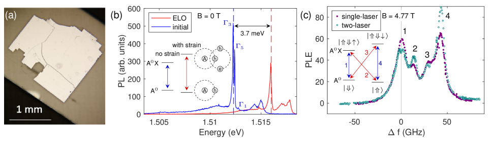
The strained sample consists of a 2 µm (001) -type GaAs epitaxial layer on a MgO substrate. The GaAs layer is doped with carbon with an acceptor density of cm-3, determined from Hall measurements. The GaAs is transferred and bonded to the MgO substrate through an epitaxial lift-off (ELO) process at room temperature (see Appendix A). Compressive strain is introduced to GaAs when the sample is cooled down to 1.5 K due to the different thermal expansion rate of GaAs and MgO. The MgO substrate is chosen as the carrier as it is transparent at the band gap of GaAs and can produce significant compressive strain. An optical microscope image of the transferred GaAs epitaxial layer on MgO is shown in Fig. 1(a). We note that this ELO method is not ideal; some cracking is observed, and possible slippage between the membrane and substrate can result in both strain reduction and strain inhomogeneity.
The photoluminescence (PL) of the sample is studied using a home-built confocal microscope with a resolution of 1 µm. The sample is cooled to 1.5 K in a helium-immersion magnetic cryostat (Janis SOM). The hole spin states are controlled and measured with two tunable continuous-wave Ti:Sapphire lasers (Spectra-Physics Matisse and Coherent 899-21). In pulsed experiments, the laser pulse is generated by passing the laser through an acousto-optic modulator (Gooch&Housego) with an on/off extinction ratio .
III Induced strain and Photoluminescence properties
| (eV) | (eV) | (eV) | |
| -7.17 | 1.16 | 0.4526 | -1.7 |
Figure 1(b) shows the PL spectra before and after ELO at 0 T and 1.5 K. The main sharp peaks are from the transitions between the acceptor bound exciton (A0X) and the neutral acceptor (A0) states. In the unstrained sample, three acceptor peaks , and are observed due to the different hh and lh states for the two holes in A0X, with the energy splitting due to hole-hole coupling and the crystal field [13]. As compressive strain introduces a hh-lh splitting and a hh-like ground state, the two holes in A0X will be in the hh spin-singlet state, which corresponds to the single acceptor peak in the PL spectrum of the strained sample. Compared with the unstrained sample, a 3.7 meV blue shift of the acceptor transition is observed. This energy shift is mainly caused by the shift of conduction and valence bands under strain and can be used as an estimate for the change in band gap energy. The strain is estimated from the energy shift by , where and are the deformation potentials that determine the conduction and valence band shift, and are the components of the elastic stiffness tensor in GaAs, see Table 1. From this, we obtain the value of the in-plane strain in our sample . This strain leads to the splitting of the heavy and light holes subbands , where is the valence-band deformation potential that determines the hh-lh splitting. We find meV for GaAs parameters 111In these estimates we disregarded the renormalization of the deformation potential due to the Coulomb potential of the acceptor [31], this effect is discussed in more detail below in relation to the spin-flip of the hole.. Since the splitting is positive for compressive strain, and is much larger than the 0.13 meV thermal energy at 1.5 K, the majority of the holes populate the hh-like state.
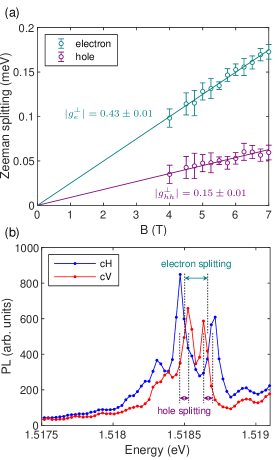
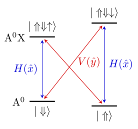
The strained sample is studied in an in-plane magnetic field (). As shown in the inset of Fig. 1(c), there are four allowed optical transitions: transition 1 (), transition 2 (), transition 3 (), and transition 4 (). Here, () and () denote the eigenstates of the electron and hole in the in-plane field. The splitting between states and is due to the hole Zeeman splitting. The splitting between states and is due to the electron Zeeman splitting, as the two holes are in a spin singlet state. As shown by the PL spectra in Appendix C, transitions 1 and 4 are horizontally polarized (parallel to the magnetic field), while transitions 2 and 3 are vertically polarized (perpendicular to the magnetic field). The selection rules (Appendix D), together with the reasonable assumption for the electron -factor, yield . The measured electron and hole g-factors are thus and .
A single-laser photoluminescence excitation (PLE) spectrum is taken to resolve all four transitions, as shown in Fig. 1(c). The single-laser PLE spectrum is taken by scanning a laser across the A0X transitions and collecting the signal from the two-hole transitions (THT). In order to excite all four transitions, the laser is linearly polarized at 45∘ with respect to the magnetic field. From the spectrum, the inhomogenous linewidth of the acceptor transitions is 10 GHz. A two-laser PLE spectrum is taken to confirm the validity of the energy diagram shown in the inset of Fig. 1(c). In the two-laser PLE spectrum, one laser is fixed at transition 1 and a second laser is scanned across all four transitions. Compared to the single-laser PLE, there is a decrease in signals from transitions 1 and 3, and an enhancement of transitions 2 and 4. These changes are consistent with the effect of optical pumping where the fixed laser pumps the spin states from to . Signals from transitions 1 and 3 (2 and 4) decrease (increase) as the intensity of these two transitions are proportional to the population in (). Additionally, a small dip in peak 1 is observed which is attributed to spectral hole burning. A fit of the dip shows a homogeneous linewidth of 1 GHz, corresponding to a 0.2 ns A0X radiative lifetime, which is in reasonable agreement with experimental measurements [13]. A small dip in peak 2 is expected due to CPT which will be further discussed in Section V. However, due to the scan resolution, the CPT dip is not clearly resolved in this spectrum.
IV Optical pumping and T1 measurement
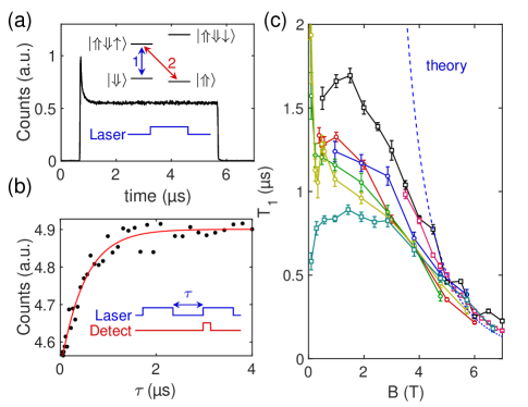
In the AX system, the A0 holes can be initialized to a certain spin state by optical pumping. As shown in Fig. 2(a), a 5 µs laser pulse is applied resonantly on transition 1 so the spin states are pumped from spin to spin . The PL signal from transition 2, which is proportional to the population of , is recorded during the optical pumping pulse. A decrease of the spin population is observed, indicating partial spin initialization is achieved.
The spin relaxation time T1 is measured by initializing the spin to , and measuring the recovery of the PL from transition 2 as a function of variable time . A single exponential fit is used to extract T1 from the recovery curve, as shown in Fig. 2(b). T1 as function of magnetic field at different spots on the sample is shown in Fig. 2(c). Between 5 and 7 T, the T1 at different spots is similar, following approximately a B-3 dependence. At these high fields, we attribute the spin relaxation of holes to the admixture mechanism resulting from the hh-lh mixing by magnetic field and a hole-phonon interaction through the deformation potentials. The detailed theory is discussed in Sec. VI. The calculation based on this theory matches the experimental result, as shown in Fig. 2(c). T1 longer than 100 µs has been measured in self-assembled InGaAs quantum dots due to the much larger hh-lh splittings [16]. Such long T1 can potentially also be achieved in the acceptor system by applying stronger and more homogeneous strain, which could be realized with other strain engineering techniques such as wafer bonding [19] or using piezoelectric actuators [20].
Below 5 T, T1 is noticeably different at different locations on the sample and does not have a clear B-field dependence. A possible mechanism to explain this behavior is a combination of a hole-hole exchange interaction and inhomogeneous hyperfine fields, which is shown to be a mechanism for T1 of donors at low fields [21]. This interaction depends on the local environment, which can vary across the sample.
V Coherent population trapping and the spin decoherence time T
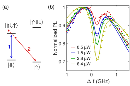
Next, we perform coherent population trapping (CPT) on the A0-A0X system to investigate the hole-spin coherence properties. As shown in Fig. 3(a), the A0X state , together with the two A0 states, and , form a -system. With a control laser driving the transition 1 () and a probe laser driving the transition 2 (), a destructive interference occurs when the energy difference between the two lasers equals the hole Zeeman splitting. On two-laser resonance, the system is pumped into a dark state, i.e. a superposition state between and [22, 23].
In our experiment, CPT is revealed by the two-laser PLE spectrum. The energy of the control laser is fixed near the resonance of transition 1 and the probe laser is scanned across the transition 2. A dip in the PLE spectrum occurs when the probe laser is on resonance with transition 2, as shown in Fig. 3(b). The linewidth and depth of the dip depend on the laser powers, the spontaneous emission rate of the state, and the dephasing rate between and . The CPT phenomenon is simulated by solving the master equation of a 3-level density matrix considering all relaxation and dephasing terms (see Appendix E).
In Fig. 3, the CPT curves at different probe powers are simultaneously fit with the density matrix model. The inhomogeneous dephasing time T between the two spin states is found to be 7 ns. The measured T in our sample is significantly smaller than the 100 ns T measured in single III-V quantum dots [5, 6]. We attribute the short T to g-factor broadening due to strain inhomogeneity in the sample. The 7 ns T corresponds to a 0.2% broadening of the in-plane hole g-factor . This g-factor broadening introduces inhomogeneity to the spin splitting between and , and hence to the spin procession frequency, which leads to a stronger dephasing. In Appendix F we calculate the intrinsic spin dephasing time due to dipole-dipole hyperfine interaction to be ns. This longer coherence time could be achieved by using strain engineering techniques that provide more homogeneous strain.
VI Theory of the heavy-hole longitudinal spin relaxation time T1
VI.1 Wave functions of acceptor-bound holes
The acceptor-bound hole states in cubic semiconductors are determined by an interplay of the spin-orbit interaction and the Coulomb energy. Before calculating the spin relaxation times, we establish the form of the hole wavefunctions and Zeeman effect in the studied system where strain is present.
In the spherical approximation, the hole bound to an acceptor is described by the total angular momentum , which is the sum of the free-hole angular momentum ( originating from the valence band Bloch functions) and the orbital momentum of the hole moving in the Coulomb field of an acceptor. In the ground state of the hole, and [24, 25]. In the absence of external fields, this state is four-fold degenerate with respect to the projection of the total angular momentum . The corresponding wave functions are [24, 25]
| (1) | ||||
where are the spherical harmonic functions, and are the radial parts of the envelope functions, and are the Bloch functions of the band. Throughout Sec. VI we use the hole representation for the hole wave functions and energies in contrast to the discussion of selection rules and energy diagrams where we used the electron representation. Note, however, that the sign of the hole -factor, as well as the final answer for , is independent of the representation used.
Now let us consider the effect of strain and magnetic field on the ground acceptor state. The biaxial strain induces the splitting between and states discussed in Sec. III. Since the estimated value of this splitting ( meV) is much smaller than the hole binding energy ( meV) [24, 13], it is possible to neglect the coupling of the ground acceptor state to the excited ones and consider the quadruplet (1) only. In the presence of strain and magnetic field , the Hamiltonian describing the ground state of an acceptor-bound hole in the basis (Eq. 1) reads
| (2) |
Here is the strain-induced splitting between and doublets, is the -factor of an acceptor-bound hole in the absence of strain (accounting for the Coulomb effects) [26, 27], are the matrices of the angular momentum , and is the Bohr magneton.
The Hamiltonian (2) does not yield linear in splitting of doublet, observed in the experiment, see Sec. III, and is insufficient to describe the experimental data. A nonzero heavy-hole in-plane -factor results from cubic symmetry terms allowed in zinc-blende semiconductors, however these terms are small, since they originate from the coupling with remote electronic bands [28]. Larger values of might result from the presence of anisotropic in-plane strain, i.e. nonzero or components of the strain tensor, in our sample. This anisotropic strain might be attributed to imperfect bonding between the GaAs epitaxial layer and the MgO substrate. The experimentally observed selection rules are consistent with (Appendix D), and therefore we consider the case , in the following. In this case, the hole Hamiltonian has the form
| (3) |
where the additional term accounts for the anisotropic in-plane strain in the sample.
The Hamiltonian (3) couples the states resulting in the splitting of the doublet. As a result, the new states and with energies are formed. At , relevant to experimental conditions, the corresponding transverse -factor and wave functions of the heavy-hole states are
| (4) |
| (5) | |||
We stress that in Eqs. (4) and (5) the Zeeman energy and the strain-induced coupling parameter can be comparable in magnitude.
VI.2 The rate of spin-flip transitions
Similarly to the case of localized electrons [4], the spin-flip transitions between the bound hole states in sufficiently strong magnetic field where the Zeeman splitting exceeds by far the hyperfine coupling is controlled by the hole-phonon interaction. In moderate magnetic fields studied here, the transitions are mediated by acoustic phonons which can give or take Zeeman energy in the course of spin relaxation. The interaction of Zeeman sublevels with an acoustic phonon is possible since the heavy-hole states have an admixture of light holes in the presence of magnetic field, as follows from Eq. (5). Hence, these states are coupled under phonon-induced deformation through the Bir-Pikus Hamiltonian [29]. Here the complex valence band structure facilitates direct spin-phonon interaction.
The spin-flip transition rates are found using Fermi’s golden rule, e.g. the rate of a transition with emission of a phonon is
| (6) |
where is the spin-flip matrix element, is the phonon wave vector, and is the speed of sound in the phonon branch . The spin-flip matrix element is , where is the Bir-Pikus Hamiltonian [30], which in the basis (1) reads
| (7) |
Here , and are the valence-band deformation potentials modified by the Coulomb interaction, [31]. The phonon-induced deformation results in the strain components
| (8) |
where is the polarization vector, is the phonon frequency, is the mass density, and is the phonon creation operator. For LA phonons, , whereas for TA phonons, there are two modes with and , where . Further we use the long wavelength approximation for the phonons, i.e. .
At zero temperature (when no phonons are present) it follows from Eqs. (5), (7) and (8) that
| (9) |
where for simplicity we used the spherical approximation for the Bir-Pikus Hamiltonian. Note that in agreement with time-reversal symmetry, the spin-flip matrix-element is proportional to , so that only magnetic-field induced admixture of light holes in the states (5) is relevant for the spin-flip process. The spin-flip rate calculated after Eqs. (6) and (9) is
| (10) |
where we used Eq. (4) to exclude unknown parameter and the relation .
The measured spin relaxation time T1 is related to the spin-flip rate at zero temperature as [21]:
| (11) |
where , and is the thermal energy. In the whole range of applied magnetic fields , and hence, . The values of the parameters used to calculate T1 are listed in Table 2. With , so that , the theoretical curve agrees well with the measured data at high fields, shown in Fig. 2(c). It corresponds to , and using the measured value of we estimate . This agrees with the values from literature which have reported hole -factors ranging from 0.52 to 2.34 [32, 27, 33].
VII conlusion
We have introduced compressive strain into a p-type GaAs epitaxial layer through the epitaxial lift-off technique. This strain breaks the degeneracy of heavy and light hole states, leading to µs-scale longitudinal spin relaxation times T1 of the heavy hole. Coherent population trapping measurements indicate a 7 ns hole spin dephasing time T in this strained sample. We quantitatively explain the measured T1 and T values based on two different mechanisms. The measured T1 is explained by a hole-phonon interaction mediated by heavy-hole light-hole mixing in the in-plane magnetic field, and the measured T is explained by in-plane hole g-factor broadening due to strain inhomogeneity. Other strain engineering techniques such as wafer bonding [19] or piezoelectric actuators [20] can possibly provide stronger and more homogeneous strain in the sample, which can potentially enhance both T1 and T in the acceptor-hole system.
Acknowledgements.
This material is based upon work supported by the National Science Foundation under Grant Nos. 1150647 and 1820614. M.V.D. acknowledges financial support from the Basis Foundation for the Advancement of Theoretical Physics and Mathematics and the Russian Federation President Grant No. MK- 2943.2019.2. M.M.G. was partially supported by the Saint-Petersburg State University for a research Grant # 51125686.Appendix A ELO process
In the strained sample, the GaAs epitaxial layer is transferred to the MgO substrate through an ELO technique. The as-grown GaAs sample contains a 2 µm p-type GaAs epitaxial layer with 50 nm Al0.2Ga0.8As cladding and an 100 nm AlAs sacrificial layer for ELO, with all those layers on a GaAs substrate. The AlAs sacrificial layer is selectively etched in 5% hydrofluoric acid for 24 hours to release the 2 µm GaAs epitaxial layer from the GaAs substrate. A 1 mm thick photoresist layer is applied to the membrane before the etching for protection. The photoresist needs to be mm thick so the GaAs epitaxial layer can bend with a small angle to let the acid etch in. After the etching, the membrane is transferred to a beaker with water for cleaning and then to an MgO substrate. A thin paper tissue is used to wick the water out from between the epitaxial layer and the MgO substrate. The sample is then put in a SPI membrane box to add pressure on top of the GaAs epitaxial layer to improve bonding with the new substrate. After waiting for 3 days, the sample is taken out and the photoresist on top of the epitaxial layer is removed in hot solvent.
Appendix B Spectrum of THT
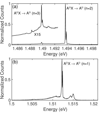
The two hole transitions (THT) are the transitions from the A0X to higher orbital states of A0. The wave function A0 is hydrogen like. The main donor lines are from A0X to n=1 states of A0. The THT transitions are from A0X to n1 states of A0, as shown in Fig. 4. For all the PLE spectra, we collect the signal from the n=2 THT transitions.
Appendix C In-plane g factors
The absolute values of the measured in-plane hole and electron -factors are and , as shown in Fig. 5. This values are close to the values measured in InGaAs/GaAs quantum dots [34]. The sign of both the electron and hole -factors is negative, as shown in Appendix D.
Appendix D selection rules
The selection rules are derived using the same method in Ref. [13]. At zero magnetic field, the eigen functions for electrons are
| (12) | |||
where is the orbital function for electrons. The eigen functions for heavy holes are
| (13) | |||
where is the orbital function for hole. Note that we use the definition in which means missing of a spin up electron so its angular momentum is negative. In an in-plane magnetic field (), the electron states become
| (14) | |||
Assuming a non-zero and a zero , the hole states in magnetic fields become
| (15) | |||
The dipole matrix element for the recombination of the electron state and hole state is . The dipole operator is , where is the electron charge and is the space vector. The calculated results of the four are shown below:
| (16) |
where . The intensity of the optical transition between electron state and hole state is proportional to , where is the electric field vector. In this Voigt geometry, and are the horizontal and vertical directions. Equation (16) indicates two transitions are polarized in horizontal direction and two transitions are polarized vertical direction, which matches with our experimental data. Figure 5(b) shows that the two transitions with horizontal polarization are at the highest and lowest energy of the four allowed transitions. As the electron -factor is negative, to match with this data, the hole -factor needs to be negative. The corresponding energy diagram of the acceptor system under magnetic fields is shown in Fig. 6. We note that we use the notation that the recombination of hole and electron represents the transition of .
Assuming a zero and a non-zero , the hole states in magnetic fields become
| (17) | |||
The corresponding calculated results of the four are shown below:
| (18) |
This indicates two transitions are polarized in 45 degree direction () and two transitions are polarized in -45 degree direction (). However, this selection rules contradict with our PL measurements shown in Fig. 5(b). Therefore, we use a non-zero and a zero in the calculation of T1.
Appendix E Density matrix model for CPT
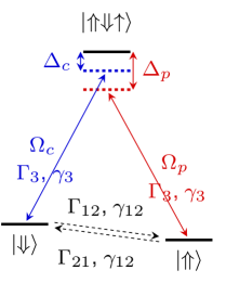
In our experiment, the states , , and are used to form the system, as shown in Fig. 7. The evolution of the system can be simulated by solving the master equation . In the equation, H is the Hamiltonian of the system
| (19) |
where and is the detuning of the probe and control laser. L is the Lindblad operator including the relaxation and dephasing between different states
| (20) | ||||
and are spin relaxation rate between and . The spin relaxation time satisfies
| (21) | |||
| (22) |
where is the hole Zeeman splitting and is the thermo energy. is the dephasing rate between and . and are the spin relaxation rate and dephasing rate between the excited state and the ground spin states. For simplicity, we assume they are the same for and . and are the detuning and strength of the control laser. and are the detuning and strength of the probe laser. The population of the excited state after equilibrium is calculated as the final result, which is proportional to the detected PL intensity in the two-laser PLE experiment. All important fitting parameters and the fitting results are shown in Table 3.
| parameter | fit values |
| T (ns) | |
| T1 (µs) | |
| (GHz) | |
| (GHz) | |
| (GHz2/µW) | |
| (GHz) | |
Appendix F Theory of the inhomogeneous dephasing time T due to hyperfine interaction with nuclear spins
The hole spin dephasing originates from the dipole-dipole part of the hyperfine interaction. In bulk semiconductors it is given by the Hamiltonian acting on the -component envelope function [4]
| (23) |
where is the crystal sublattice index, enumerates nuclei in a given sublattice, is the volume of the unit cell, is the position of th nucleus in the sublattice , is the conduction band hyperfine coupling constant, is the spin of the nucleus, and we recall that is the free-hole angular momentum and we use the notation . In Eq. (23) and are the dimensionless parameters with resulting from the cubic symmetry of the crystal. Depending on the material system and isotope in question the parameters and can be comparable [4, 35, 36]. Hereafter, for simplicity, we take into account the contribution of the only: As we see below it already produces right order-of-magnitude of the dephasing time.
In our experiments, the hole spin dephasing is studied in the Voigt configuration where . In the external field along the -axis, the hole-states and are given by Eq. (5) with the and basis functions given by the general expressions (1). Provided that the field is sufficiently strong, i.e., under the conditions where the hole Zeeman splitting in the magnetic field, , Eq. (4), exceeds by far the splittings induced by the nuclear spin fluctuations, the dephasing is controlled by the nuclear field fluctuations in the directions of the hole pseudospin. We calculate , the contribution to Larmor frequency due to nuclei, as
| (24) |
The analysis shows that it contains -independent and terms, the latter are neglected. Correspondingly, the mean square fluctuation of nuclear field is
| (25) |
where , and . Here we took into account that . Summation by can be changed to the integration using the standard expression
| (26) |
Using this formula and taking into account that nuclei in GaAs have the same spin , we finally obtain
| (27) |
The compact analytical expression for the can be derived assuming that exceeds by far in Eqs. (1). Keeping the terms with the lowest powers of we arrive at
| (28) |
It is noteworthy that Eq. (28) contains two contributions. The second one is related to the heavy-light hole mixing due to the strain and is similar to the one widely studied in quantum dot structures [37, 4]. The first contribution results from the complex structure of the acceptor function. This contribution does not require any strain.
Assuming the Gaussian distribution of the nuclear field fluctuations [38], the component of the hole pseudospin normal to magnetic field decays as , the corresponding decay time . Using Eq. (28), eV, eV [37], , , , where is the acceptor Bohr radius [24], we obtain ns for the first contribution in Eq. (28) and ns for the second contribution in Eq. (28).
References
- Kloeffel and Loss [2013] Christoph Kloeffel and Daniel Loss, “Prospects for spin-based quantum computing in quantum dots,” Annual Review of Condensed Matter Physics 4, 51–81 (2013).
- Morello et al. [2020] Andrea Morello, Jarryd J. Pla, Patrice Bertet, and David N. Jamieson, “Donor spins in silicon for quantum technologies,” Advanced Quantum Technologies 3, 2000005 (2020).
- Linpeng et al. [2018] Xiayu Linpeng, Maria L.K. Viitaniemi, Aswin Vishnuradhan, Y. Kozuka, Cameron Johnson, M. Kawasaki, and Kai-Mei C. Fu, “Coherence properties of shallow donor qubits in ZnO,” Physical Review Applied 10, 064061 (2018).
- Glazov [2018] M.M. Glazov, Electron & Nuclear Spin Dynamics in Semiconductor Nanostructures, Series on Semiconductor Science and Technology (OUP Oxford, 2018).
- Brunner et al. [2009] Daniel Brunner, Brian D. Gerardot, Paul A. Dalgarno, Gunter Wüst, Khaled Karrai, Nick G. Stoltz, Pierre M. Petroff, and Richard J. Warburton, “A coherent single-hole spin in a semiconductor,” Science 325, 70 (2009).
- Prechtel et al. [2016] Jonathan H. Prechtel, Andreas V. Kuhlmann, Julien Houel, Arne Ludwig, Sascha R. Valentin, Andreas D. Wieck, and Richard J. Warburton, “Decoupling a hole spin qubit from the nuclear spins,” Nature Materials 15, 981 (2016).
- Xu et al. [2008] Xiaodong Xu, Bo Sun, Paul R. Berman, Duncan G. Steel, Allan S. Bracker, Dan Gammon, and L. J. Sham, “Coherent population trapping of an electron spin in a single negatively charged quantum dot,” Nature Physics 4, 692 (2008).
- Fu et al. [2005] Kai-Mei C. Fu, Charles Santori, Colin Stanley, M. C. Holland, and Yoshihisa Yamamoto, “Coherent population trapping of electron spins in a high-purityn-type GaAs semiconductor,” Physical Review Letters 95 (2005), 10.1103/physrevlett.95.187405.
- Greve et al. [2011] Kristiaan De Greve, Peter L. McMahon, David Press, Thaddeus D. Ladd, Dirk Bisping, Christian Schneider, Martin Kamp, Lukas Worschech, Sven Höfling, Alfred Forchel, and Yoshihisa Yamamoto, “Ultrafast coherent control and suppressed nuclear feedback of a single quantum dot hole qubit,” Nature Physics 7, 872 (2011).
- Delteil et al. [2015] Aymeric Delteil, Zhe Sun, Wei bo Gao, Emre Togan, Stefan Faelt, and Ataç Imamoğlu, “Generation of heralded entanglement between distant hole spins,” Nature Physics 12, 218 (2015).
- Watzinger et al. [2018] Hannes Watzinger, Josip Kukučka, Lada Vukušić, Fei Gao, Ting Wang, Friedrich Schäffler, Jian-Jun Zhang, and Georgios Katsaros, “A germanium hole spin qubit,” Nature Communications 9, 3902 (2018).
- Maurand et al. [2016] R. Maurand, X. Jehl, D. Kotekar-Patil, A. Corna, H. Bohuslavskyi, R. Laviéville, L. Hutin, S. Barraud, M. Vinet, M. Sanquer, and S. De Franceschi, “A CMOS silicon spin qubit,” Nature Communications 7, 13575 (2016).
- Karin et al. [2015] Todd Karin, Russell J. Barbour, Charles Santori, Yoshihisa Yamamoto, Yoshiro Hirayama, and Kai-Mei C. Fu, “Radiative properties of multicarrier bound excitons in GaAs,” Phys. Rev. B 91, 165204 (2015).
- Hilton and Tang [2002] D. J. Hilton and C. L. Tang, “Optical orientation and femtosecond relaxation of spin-polarized holes in GaAs,” Phys. Rev. Lett. 89, 146601 (2002).
- Viña et al. [1992] L. Viña, T.C. Damen, J.E. Cunningham, J. Shah, and L.J. Sham, “Spin relaxation dynamics in GaAs quantum wells: Free carriers and excitons,” Superlattices and Microstructures 12, 379 (1992).
- Heiss et al. [2007] D. Heiss, S. Schaeck, H. Huebl, M. Bichler, G. Abstreiter, J. J. Finley, D. V. Bulaev, and Daniel Loss, “Observation of extremely slow hole spin relaxation in self-assembled quantum dots,” Phys. Rev. B 76, 241306 (2007).
- Chuang [2009] Shun Lien Chuang, Physics of Photonic Devices (Wiley, 2009).
- Note [1] In these estimates we disregarded the renormalization of the deformation potential due to the Coulomb potential of the acceptor [31], this effect is discussed in more detail below in relation to the spin-flip of the hole.
- Stanton et al. [2020] Eric J. Stanton, Jeff Chiles, Nima Nader, Galan Moody, Nicolas Volet, Lin Chang, John E. Bowers, Sae Woo Nam, and Richard P. Mirin, “Efficient second harmonic generation in nanophotonic GaAs-on-insulator waveguides,” Optics Express 28, 9521 (2020).
- Yuan et al. [2018] Xueyong Yuan, Fritz Weyhausen-Brinkmann, Javier Martin-Sanchez, Giovanni Piredda, Vlastimil Křápek, Yongheng Huo, Huiying Huang, Christian Schimpf, Oliver G. Schmidt, Johannes Edlinger, Gabriel Bester, Rinaldo Trotta, and Armando Rastelli, “Uniaxial stress flips the natural quantization axis of a quantum dot for integrated quantum photonics,” Nat. Commun. 9, 3058 (2018).
- Linpeng et al. [2016] Xiayu Linpeng, Todd Karin, M. V. Durnev, Russell Barbour, M. M. Glazov, E. Ya. Sherman, S. P. Watkins, Satoru Seto, and Kai-Mei C. Fu, “Longitudinal spin relaxation of donor-bound electrons in direct band-gap semiconductors,” Physical Review B 94, 125401 (2016).
- Harris [1997] Stephen E. Harris, “Electromagnetically induced transparency,” Physics Today 50, 36–42 (1997).
- Agap’ev et al. [1993] B D Agap’ev, M B Gornyi, B G Matisov, and Yu V Rozhdestvenskii, “Coherent population trapping in quantum systems,” Physics-Uspekhi 36, 763 (1993).
- Baldereschi and Lipari [1973] A. Baldereschi and Nunzio O. Lipari, “Spherical model of shallow acceptor states in semiconductors,” Phys. Rev. B 8, 2697 (1973).
- Gelmont and Dyakonov [1972] B. L. Gelmont and M. I. Dyakonov, “Acceptor levels in dyamond-type semiconductors,” Sov. Phys. Semicond. 5, 1905 (1972).
- Gel’mont and Dyakonov [1973] B. L. Gel’mont and M. I. Dyakonov, “-factor of acceptors in zinc-blende semiconductors,” Sov. Phys. Semicond. 7, 1345 (1973).
- Malyshev and Merkulov [1997] A. V. Malyshev and I. A. Merkulov, “Magnetic moment of an acceptor center in cubic semiconductors,” Phys. Solid State 39, 49 (1997).
- Marie et al. [1999] X. Marie, T. Amand, P. Le Jeune, M. Paillard, P. Renucci, L. E. Golub, V. D. Dymnikov, and E. L. Ivchenko, “Hole spin quantum beats in quantum-well structures,” Phys. Rev. B 60, 5811 (1999).
- Woods et al. [2004] L. M. Woods, T. L. Reinecke, and R. Kotlyar, “Hole spin relaxation in quantum dots,” Phys. Rev. B 69, 125330 (2004).
- Bir and Pikus [1974] G. L. Bir and G. E. Pikus, Symmetry and strain-induced effects in semiconductors (Wiley, New York, 1974).
- Kogan and Polupanov [1981] Sh. M. Kogan and A. F. Polupanov, “Optical absorption and photoeffect spectra of shallow acceptor impurities in semiconductors,” Zh. Eksp. Teor. Fiz. 80, 394 (1981).
- Bimberg [1978] D. Bimberg, “Anomaly of the linear and quadratic zeeman effect of an effective-mass acceptor: C in GaAs,” Phys. Rev. B 18, 1794 (1978).
- Kirpichev et al. [1996] V. E. Kirpichev, I. V. Kukushkin, V. E. Bisti, K. von Klitzing, and K. Eberl, “Magnetooptic measurements of the cyclotron mass and g-factor of light holes in GaAs,” Jetp Lett. 64, 814 (1996).
- Tholen et al. [2019] H. M. G. A. Tholen, J. S. Wildmann, A. Rastelli, R. Trotta, C. E. Pryor, E. Zallo, O. G. Schmidt, P. M. Koenraad, and A. Yu. Silov, “Active tuning of the g-tensor in InGaAs/GaAs quantum dots via strain,” Phys. Rev. B 99, 195305 (2019).
- Chekhovich et al. [2013] E. A. Chekhovich, M. M. Glazov, A. B. Krysa, M. Hopkinson, P. Senellart, A. Lemaitre, M. S. Skolnick, and A. I. Tartakovskii, “Element-sensitive measurement of the hole-nuclear spin interaction in quantum dots,” Nat Phys 9, 74–78 (2013).
- Vidal et al. [2016] M. Vidal, M. V. Durnev, L. Bouet, T. Amand, M. M. Glazov, E. L. Ivchenko, P. Zhou, G. Wang, T. Mano, T. Kuroda, X. Marie, K. Sakoda, and B. Urbaszek, “Hyperfine coupling of hole and nuclear spins in symmetric (111)-grown gaas quantum dots,” Phys. Rev. B 94, 121302 (2016).
- Testelin et al. [2009] C. Testelin, F. Bernardot, B. Eble, and M. Chamarro, “Hole–spin dephasing time associated with hyperfine interaction in quantum dots,” Physical Review B 79, 195440 (2009).
- Merkulov et al. [2002] I. A. Merkulov, Al. L. Efros, and M. Rosen, “Electron spin relaxation by nuclei in semiconductor quantum dots,” Physical Review B 65, 205309 (2002).