Quantum Spin Hall Effect in TaTe5 ( Pd, Ni)
Abstract
Quantum spin Hall (QSH) effect with great promise for the potential application in spintronics and quantum computing has attracted extensive research interest from both theoretical and experimental researchers. Here, we predict monolayer Ta2Pd3Te5 can be a QSH insulator based on first-principles calculations. The interlayer binding energy in the layered van der Waals compound Ta2Pd3Te5 is 19.6 meV/Å2; thus, its monolayer/thin-film structures could be readily obtained by exfoliation. The band inversion near the Fermi level () is an intrinsic characteristic, which happens between Ta- and Pd- orbitals without spin-orbit coupling (SOC). The SOC effect opens a global gap and makes the system a QSH insulator. With the - band-inverted feature, the nontrivial topology in monolayer Ta2Pd3Te5 is characterized by the time-reversal topological invariant , which is computed by the one-dimensional (1D) Wilson loop method as implemented in our first-principles calculations. The helical edge modes are also obtained using surface Green’s function method. Our calculations show that the QSH state in TaTe5 ( Pd, Ni) can be tuned by external strain. These monolayers and thin films provide feasible platforms for realizing QSH effect as well as related devices.
I introduction
A quantum spin Hall (QSH) insulator is a novel state of two-dimensional (2D) quantum matter that is interesting for both fundamental condensed matter physics and materials science. It has an insulating 2D bulk but conducting edge states. The backscattering channel for such edge states is prohibited by time-reversal symmetry (TRS). The dissipationless conducting channels make it promising to realize low-power consumption electronics and spin-polarized current. In addition, on the interface of a conventional superconductor and a QSH insulator, superconducting proximity effect can lead to the appearance of topological superconductivity and Majorana fermions Fu and Kane (2008), which can be used for topological quantum computation Nayak et al. (2008). Due to these wide-ranging and fascinating applications, the QSH insulator has become one of the most hot and fruitful fields in condensed matter physics.
In despite of many proposals for QSH insulators Liu et al. (2011); Si et al. (2014); Xu et al. (2013); Zhang et al. (2018); Ma et al. (2015); Zhou et al. (2014); Luo and Xiang (2015); Weng et al. (2014); Qian et al. (2014), the QSH state has been confirmed in very few systems, such as quantum well structures of HgTe/CdTe König et al. (2007) and InAs/GaSb Knez et al. (2011), and monolayer 1T’-WTe2 Tang et al. (2017); Wu et al. (2018). On the other hand, atomic monolayers of van der Waals materials (vdW monolayers) have intrigued various study of 2D materials recently, revealing a wide range of extraordinary properties and functionalities, such as 2D ferromagnetism Gong et al. (2017); Deng et al. (2018); Fei et al. (2018), Ising superconductivity Xing et al. (2017); Liu et al. (2020), and unconventional superconductivity, etc Cao et al. (2018a, b). These atomic vdW monolayers are usually quite stable and easily exfoliated due to the weak vdW interaction between adjacent layers. Owing to their atomic thickness, these 2D layers can be readily tuned through chemical and mechanical techniques. However, the vdW monolayers of the QSH state are interesting but very rare Qian et al. (2014).
In this paper, based on first-principles calculations, we find that the vdW monolayers TaTe5 ( Pd, Ni) are potential candidates for realizing QSH effect. With experimental crystal parameters, our calculations show that monolayer Ta2Pd3Te5 is a QSH insulator with a small band gap, while monolayer Ta2Ni3Te5 is trivial. After applying uniaxial strain, monolayer Ta2Ni3Te5 can be tuned into the QSH state. The interlayer binding energy in layered bulk Ta2Pd3Te5 is 19.6 meV/Å2. Resultantly, monolayer Ta2Pd3Te5 can be readily exfoliated from the bulk crystals. The - band inversion at already takes place without spin-orbit coupling (SOC). Upon including SOC effect, monolayer Ta2Pd3Te5 becomes a QSH insulator, which is characterized by the computed nonzero index with the 1D Wilson loop method Yu et al. (2011). The existence of nontrivial helical edge states is confirmed by the open-boundary calculations. Our study also shows that external strain is a good means to engineer the QSH state in monolayers TaTe5. Our findings suggest that it is promising to realize QSH effect as well as related devices in these monolayers or thin films in the future.
II Calculation method and crystal structures
The first-principles calculations were performed within the framework of the projector augmented wave (PAW) method Blöchl (1994); Kresse and Joubert (1999) implemented in Vienna ab initio simulation (VASP) package Kresse and Furthmüller (1996, 1996). The Perdew-Burke-Ernzerhof (PBE) generalized gradient approximation exchange-correlations functional Perdew et al. (1996) was implemented in calculations. The cut-off energy for plane wave expansion was 500 eV, and 1 16 4 -point sampling grids were used in the self-consistent process (as the monolayer structure was placed in the -plane in our calculations). SOC was taken into account within the second variational method self-consistently (PBE+SOC). Single crystals of Ta2Pd3Te5 were synthesized by self-flux method and the detailed crystallographic parameters were obtained by the single-crystal x-ray diffraction (XRD) study. The details of XRD study are shown in Section .1 of the supplementary materials (SM). To study the strain effect, the internal atomic positions have been fully relaxed until the residual forces on each atom were less than 0.01 eV/Å in the strained structures. The irreducible representations (irreps) were obtained by the program irvsp Gao et al. (2020). An supercell was built to calculate phonon dispersion using PHONOPY package Togo et al. (2008). The maximally localized Wannier functions (MLWFs) for the Ta-, Pd- and Te- orbitals were constructed to calculate the edge states from the surface Green’s function of the semi-infinite system based on the iterative method Sancho et al. (1984, 1985); Marzari et al. (2012). To investigate the interatomic bonding in the compounds, crystal orbital Hamilton populations (COHP) calculations were preformed using LOBSTER package Dronskowski and Blochl (1993); Deringer et al. (2011); Maintz et al. (2013, 2016a, 2016b); Nelson et al. (2020).
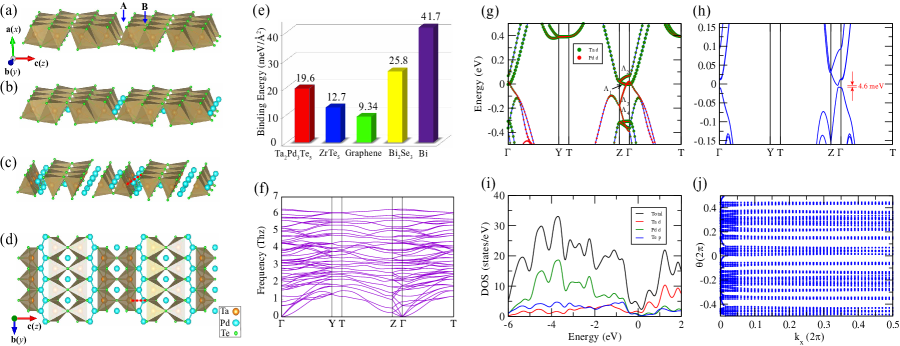
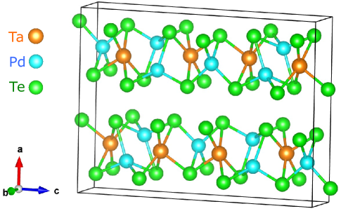
The layered vdW compound Ta2Pd3Te5 crystallizes in an orthorhombic layered structure with space group (SG) #62 ( or ) (See details in Section .1 of the SM). The bulk primitive unit cell contains two layers (i.e., -plane), which are related by inversion symmetry. The adjacent layers are connected by vdW interactions. To understand the crystal structure of monolayer TaTe5, we first construct an idealized polyhedral representation of the double chain of edge-sharing Ta ( Se, Te) octahedra, as shown in Fig. 1(a). In this double chain structure, the double chain of Ta octahedra are condensed over their apical atoms to form a Ta layer. In the Ta layer, there are two types of tetrahedral voids (i.e., A site and B site) which are capable of accepting “interstitial” metal atoms. Then, based on Ta layer, Ta2NiSe5 layer [Fig. 1(b)] can be understood by filling one A site with nickel, while TaTe5 layer [Fig. 1(c)] can be described with one A site and two B sites filled with atoms. Thus, in TaTe5 layer, the Ta atoms are actually coordinated to five Te neighbors in an approximate square pyramid at distances between 2.7 and 2.8 Å, with an additional sixth Te atom at a nonbonding [red dashed lines in Figs. 1(c) and 1(d)] Ta–Te distance of 3.9 Å due to the insertion of the Pd chain at B sites. Fig. 1(d) shows a top view of the monolayer Ta2Pd3Te5 (i.e., the projection along [100]). Whereas the metal atoms in practically all known four-coordinate palladium complexes are square-planar coordinated as a result of the strong ligand-field splitting Vanquickenborne and Ceulemans (1981), the palladium in the Ta2Pd3Te5 is coordinated tetrahedrally to the chalcogenides, which is rather unusual. The metal-metal bonding interactions between Ta and metals are of crucial rule for the electronic stability of these structures Tremel (1993), which are confirmed by our COHP calculations in Fig. 2(a).
III results and discussions
The bulk TaTe5 is of orthorhombic structure with (No. 62). The symmetry classification for SG 62 is Song et al. (2018), which are computed to be (0000) for both Ta2Pd3Te5 and Ta2Ni3Te5. However, their mirror Chern numbers in plane are computed to be nonzero. These results indicate that the bulk TaTe5 are topological crystalline insulators with trivial symmetry indicators (see more details in Section .2 of the SM). The interlayer binding energy of Ta2Pd3Te5 is computed to be about 19.6 meV/, which is smaller than of 1T’-WTe2 (28 meV/) and compatible with other layered materials Weng et al. (2014); Nie et al. (2019), as shown in Fig. 1(e). Given the weak interlayer coupling strength, monolayers and thin films of Ta2Pd3Te5 can be exfoliated easily from the bulk materials. To confirm the stability of the monolayer, its phonon spectrum has been obtained in Fig. 1(f). No imaginary frequency mode in the phonon spectrum indicates that the monolayer is dynamically stable. We focus on the results of monolayers TaTe5 in the main text and put the results of the 3D bulks in the SM.
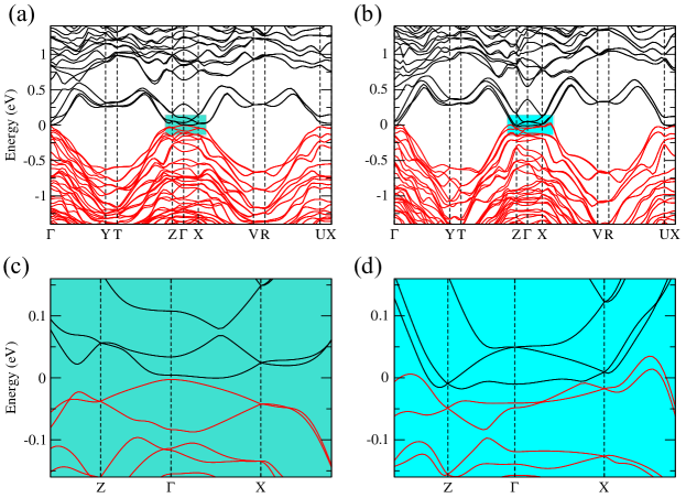
To begin with, the PBE band structure of monolayer Ta2Pd3Te5 is presented in Fig. 1(g) with different orbital weights. Along the Z– line (i.e., line), the low-energy bands near are two conduction bands ( and irreps) derived from Ta- orbitals, and two valence bands ( and irreps) originating from Pd- orbitals (neglecting the contributions from Te atoms for simplicity). The irreps are labeled by the single point group on line. The calculated density of states (DOS) are shown in Fig. 1(i) together with the partial DOS for Ta-, Pd- and Te- orbitals. The results suggest that Te- and Pd- states are occupied below , while the states above are mainly dominated by Ta- orbitals. It’s noted that the Pd- and Ta- states have strong hybridization around . The band crossing between and bands, which have different eigenvalues, results in a -protected nodal line in the 2D Brillouin zone (BZ). Thus, there are real crossing points along –Y and –T in Fig. 1(g).
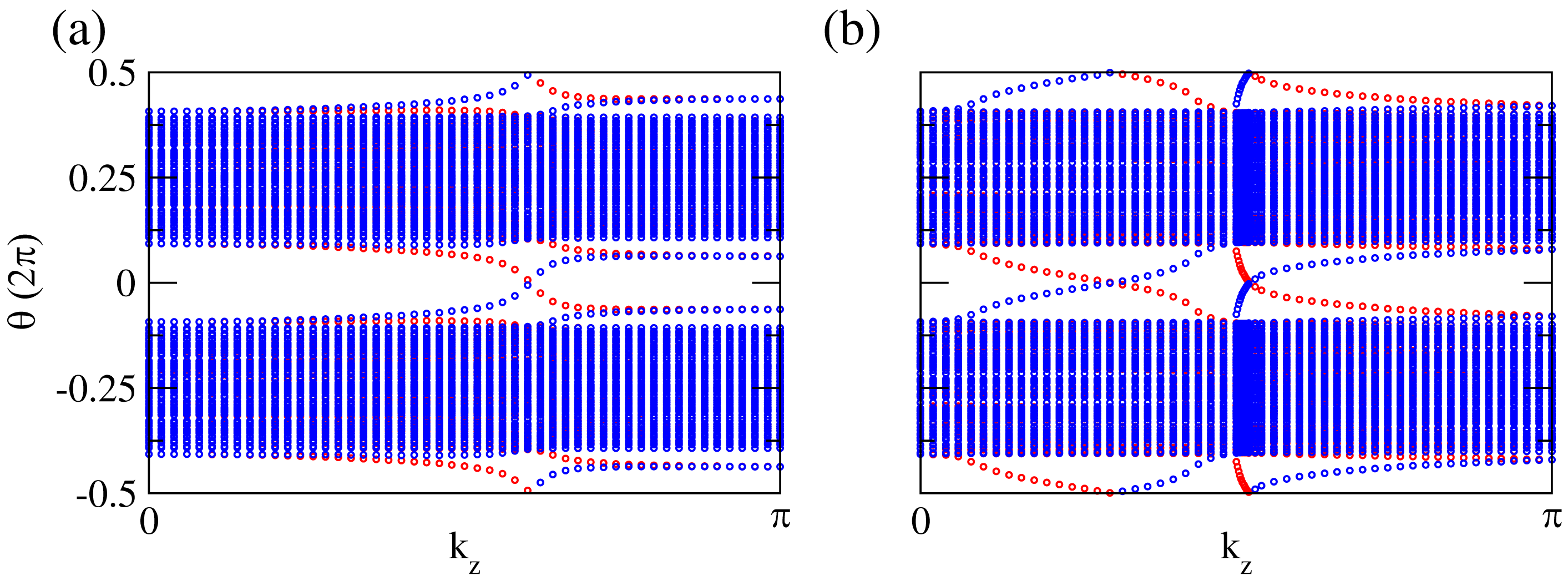
Upon including SOC, the nodal line opens a band gap ( 4.6 meV) and the system becomes an insulator, as shown in Fig. 1(h). Due to the lack of inversion symmetry, the index in monolayer Ta2Pd3Te5 is computed through the 1D Wilson loop method. The computed Wannier charge centers (WCCs) in Fig. 1(j) show a zig-zag pattern in half of the BZ, indicating that monolayer Ta2Pd3Te5 is a QSH insulator.
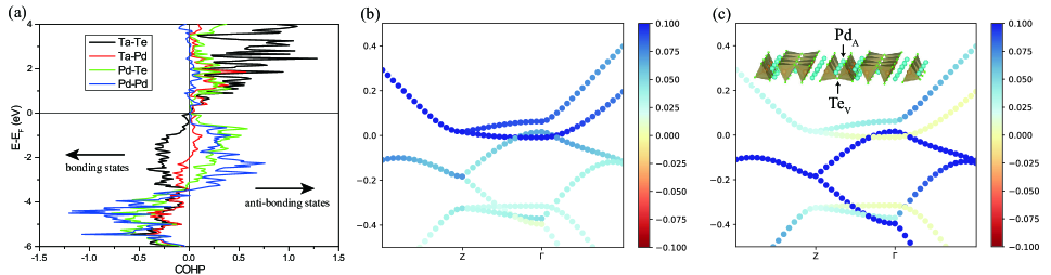
To further understand the band inversion mechanism of monolayer Ta2Pd3Te5, we calculated the COHP of Ta–Te, Ta–Pd, Pd–Pd and Pd–Te chemical bonds, as shown in Fig. 2(a). The positive and negative values of COHP indicate anti-bonding and bonding states, respectively. As expected, the bonding (anti-bonding) states of Ta–Te bands are below (above) . Additionally, the anti-bonding states of Pd–Ta and Pd–Te bonds also make many contributions below . By calculating the -dependent COHP for the low-energy bands in Figs. 2(b,c), we find that the anti-bonding states of Ta–Te bonds contribute to the two conduction bands, while the two valence bands are mainly from the anti-bonding states of PdA–TeV bonds (the Ta–Te bonding states are neglected for simplicity). Thus, we conclude that the band inversion is closely related to the PdA–TeV anti-bonding states. To further verify this conclusion, we have investigated the evolution of the band structures by changing the length of the PdA–TeV bond (i.e., simply moving PdA in -direction). The results are shown in Fig. S5. As PdA atom moves away from TeV atom, the PdA–TeV bond is weakened due to the increase of the bond length. Thus, the anti-bonding states (valence bands) move downwards energetically, which would remove the band inversion. We find that the band inversion could be an intrinsic characteristic of the A-site filled structure and already takes place without including SOC in the first-principles calculations. Our PBE calculations show that monolayers Ta2Pd3Te5 and Ta2Ni3Te5 are near the phase boundary between a trivial insulator and a QSH insulator.
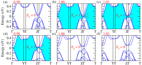
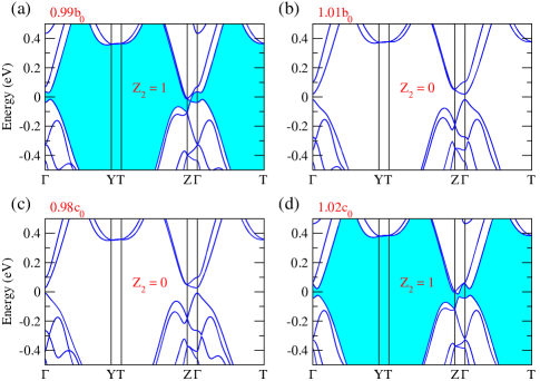
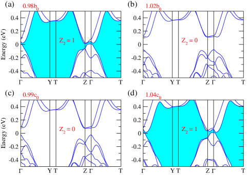
When these vdW monolayers are grown on different substrates, the strain can be easily applied on monolayer samples. Thus, we investigate the strain effect on the systems. Fig. 3 shows the PBE+SOC band structures of monolayers Ta2Pd3Te5 and Ta2Ni3Te5 under different uniaxial strains. The results show that the QSH state can be tuned by external strain. With uniaxial strain along -direction (), the band inversion (defined as ) at becomes larger, as shown in Fig. 3(c). Although monolayer Ta2Ni3Te5 is a trivial insulator without strain, it would become a QSH insulator after applying a small compressive strain along -direction () in Fig. 3(d) ( and are the lattice constants obtained by our XRD study in Section .1 of the SM). Therefore, we find that compressive strain along -direction (and tensile strain along -direction) benefits the - band inversion at and the emergence of the resultant QSH state.
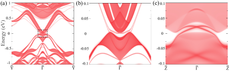
In view of the fact that the hallmark of topological nontrivial property for the QSH state is the existence of topologically nontrivial edge states. The tight-binding Hamiltonians of semi-infinite samples have been constructed by the MLWFs for Ta-, Pd- and Te- orbitals, which were extracted from the first-principles calculations for monolayer Ta2Pd3Te5 under 2% tensile strain along -direction. The imaginary parts of the surface Green’s functions show the spectrum of the edge states. The -directed and -directed edge spectra are shown in Figs. 4(a) and 4(c), respectively. In the bulk gap (Figs. 4(b-c)), there are two helical edge states connecting the bulk valence continuum to the conduction continuum, which are consistent with the nontrivial topology of the system.
As the energy band gap can be underestimated in the PBE calculations and more complicated details should be considered in the future experiments, we have the following discussions on the QSH state in TaTe5. First, the band structures are sensitive to the external strain, which provides a good means to manipulate the QSH state. Second, once considering few-layer thin films, the strength of band inversion is enhanced (see details in Section .5 of the SM), which is helpful to realize the QSH state. Third, atomic thin monolayer offers a facile mechanism to control the electronic properties by electric field in vdW devices. Last, considering layered vdW heterostructures with ferromagnetic 2D layers, they can be used to design novel topological states in the future, such as quantum anomalous Hall effect. In addition, we have undertaken scanning tunneling spectroscopy measurements. Although the details will be published separately, we note that the edge states are directly observed at the step edges of the Ta2Pd3Te5 crystals, which agree well with the QSH state of monolayer Ta2Pd3Te5.
IV CONCLUSION
In summary, we performed first-principles calculations for the electronic structures and topological property of monolayers TaTe5. The band inversion in Ta2Pd3Te5 has already happened without SOC, resulting in a nodal line surrounding , which is protected by the glide mirror . Upon including SOC, it becomes a QSH insulator with a global band gap. The invariant is computed to be 1. The helical edge states are obtained accordingly. In addition, the study of the strain effect shows that the band structures and band topology in monolayers TaTe5 can be easily tuned by uniaxial strain. The monolayer Ta2Ni3Te5 can also be a QSH insulator as well under 2% uniaxial strain along -direction. Considering the stability and transferability of the atomic layers, the monolayers and thin films of TaTe5 provide feasible platforms to study QSH effect as well as related devices.
Acknowledgements.
This work was supported by the National Natural Science Foundation of China (Grants No. 11974395, U2032204), the Strategic Priority Research Program of Chinese Academy of Sciences (Grant No. XDB33000000), and the CAS Pioneer Hundred Talents Program. Y.G. Shi acknowledges the support from Chinese National Key Research and Development Program (No. 2017YFA0302901, 2016YFA0300604), the K. C. Wong Education Foundation (GJTD-2018-01) and Beijing Natural Science Foundation (Z180008).References
- Fu and Kane (2008) L. Fu and C. L. Kane, Physical review letters 100, 096407 (2008).
- Nayak et al. (2008) C. Nayak, S. H. Simon, A. Stern, M. Freedman, and S. D. Sarma, Reviews of Modern Physics 80, 1083 (2008).
- Liu et al. (2011) C.-C. Liu, W. Feng, and Y. Yao, Phys. Rev. Lett. 107, 076802 (2011).
- Si et al. (2014) C. Si, J. Liu, Y. Xu, J. Wu, B.-L. Gu, and W. Duan, Phys. Rev. B 89, 115429 (2014).
- Xu et al. (2013) Y. Xu, B. Yan, H.-J. Zhang, J. Wang, G. Xu, P. Tang, W. Duan, and S.-C. Zhang, Phys. Rev. Lett. 111, 136804 (2013).
- Zhang et al. (2018) W. Zhang, Q. Wu, O. V. Yazyev, H. Weng, Z. Guo, W.-D. Cheng, and G.-L. Chai, Phys. Rev. B 98, 115411 (2018).
- Ma et al. (2015) Y. Ma, Y. Dai, L. Kou, T. Frauenheim, and T. Heine, Nano letters 15, 1083 (2015).
- Zhou et al. (2014) J.-J. Zhou, W. Feng, C.-C. Liu, S. Guan, and Y. Yao, Nano letters 14, 4767 (2014).
- Luo and Xiang (2015) W. Luo and H. Xiang, Nano letters 15, 3230 (2015).
- Weng et al. (2014) H. Weng, X. Dai, and Z. Fang, Physical Review X 4, 011002 (2014).
- Qian et al. (2014) X. Qian, J. Liu, L. Fu, and J. Li, Science 346, 1344 (2014), https://science.sciencemag.org/content/346/6215/1344.full.pdf .
- König et al. (2007) M. König, S. Wiedmann, C. Brüne, A. Roth, H. Buhmann, L. W. Molenkamp, X.-L. Qi, and S.-C. Zhang, Science 318, 766 (2007), https://science.sciencemag.org/content/318/5851/766.full.pdf .
- Knez et al. (2011) I. Knez, R.-R. Du, and G. Sullivan, Phys. Rev. Lett. 107, 136603 (2011).
- Tang et al. (2017) S. Tang, C. Zhang, D. Wong, Z. Pedramrazi, H.-Z. Tsai, C. Jia, B. Moritz, M. Claassen, H. Ryu, S. Kahn, et al., Nature Physics 13, 683 (2017).
- Wu et al. (2018) S. Wu, V. Fatemi, Q. D. Gibson, K. Watanabe, T. Taniguchi, R. J. Cava, and P. Jarillo-Herrero, Science 359, 76 (2018).
- Gong et al. (2017) C. Gong, L. Li, Z. Li, H. Ji, A. Stern, Y. Xia, T. Cao, W. Bao, C. Wang, Y. Wang, Z. Q. Qiu, R. J. Cava, S. G. Louie, J. Xia, and X. Zhang, Nature 546, 265 (2017).
- Deng et al. (2018) Y. Deng, Y. Yu, Y. Song, J. Zhang, N. Z. Wang, Z. Sun, Y. Yi, Y. Z. Wu, S. Wu, J. Zhu, J. Wang, X. H. Chen, and Y. Zhang, Nature 563, 94 (2018).
- Fei et al. (2018) Z. Fei, B. Huang, P. Malinowski, W. Wang, T. Song, J. Sanchez, W. Yao, D. Xiao, X. Zhu, A. F. May, W. Wu, D. H. Cobden, J.-H. Chu, and X. Xu, Nature Materials 17, 778 (2018).
- Xing et al. (2017) Y. Xing, R. Zhao, P. Shan, F. Zheng, Y. Zhang, H. Fu, Y. Liu, M. Tian, C. Xi, H. Liu, J. Feng, X. Lin, S. Ji, X. Chen, Q.-K. Xue, and J. Wang, Nano Letters 17, 6802 (2017).
- Liu et al. (2020) Y. Liu, Y. Xu, J. Sun, C. Liu, Y. Liu, C. Wang, Z. Zhang, K. Gu, Y. Tang, C. Ding, et al., Nano Letters 20, 5728 (2020).
- Cao et al. (2018a) Y. Cao, V. Fatemi, A. Demir, S. Fang, S. L. Tomarken, J. Y. Luo, J. D. Sanchez-Yamagishi, K. Watanabe, T. Taniguchi, E. Kaxiras, R. C. Ashoori, and P. Jarillo-Herrero, Nature 556, 80 (2018a).
- Cao et al. (2018b) Y. Cao, V. Fatemi, S. Fang, K. Watanabe, T. Taniguchi, E. Kaxiras, and P. Jarillo-Herrero, Nature 556, 43 (2018b).
- Yu et al. (2011) R. Yu, X. L. Qi, A. Bernevig, Z. Fang, and X. Dai, Phys. Rev. B 84, 075119 (2011).
- Blöchl (1994) P. E. Blöchl, Phys. Rev. B 50, 17953 (1994).
- Kresse and Joubert (1999) G. Kresse and D. Joubert, Phys. Rev. B 59, 1758 (1999).
- Kresse and Furthmüller (1996) G. Kresse and J. Furthmüller, Computational Materials Science 6, 15 (1996).
- Kresse and Furthmüller (1996) G. Kresse and J. Furthmüller, Phys. Rev. B 54, 11169 (1996).
- Perdew et al. (1996) J. P. Perdew, K. Burke, and M. Ernzerhof, Physical Review Letters 77, 3865 (1996).
- Gao et al. (2020) J. Gao, Q. Wu, C. Persson, and Z. Wang, arXiv preprint arXiv:2002.04032 (2020).
- Togo et al. (2008) A. Togo, F. Oba, and I. Tanaka, Phys. Rev. B 78, 134106 (2008).
- Sancho et al. (1984) M. P. L. Sancho, J. M. L. Sancho, and J. Rubio, Journal of Physics F: Metal Physics 14, 1205 (1984).
- Sancho et al. (1985) M. P. L. Sancho, J. M. L. Sancho, J. M. L. Sancho, and J. Rubio, Journal of Physics F: Metal Physics 15, 851 (1985).
- Marzari et al. (2012) N. Marzari, A. A. Mostofi, J. R. Yates, I. Souza, and D. Vanderbilt, Rev. Mod. Phys. 84, 1419 (2012).
- Dronskowski and Blochl (1993) R. Dronskowski and P. E. Blochl, Journal of Physical Chemistry 97, 8617 (1993).
- Deringer et al. (2011) V. L. Deringer, A. L. Tchougreeff, and R. Dronskowski, Journal of Physical Chemistry A 115, 5461 (2011).
- Maintz et al. (2013) S. Maintz, V. L. Deringer, A. L. Tchougreeff, and R. Dronskowski, Journal of Computational Chemistry 34, 2557 (2013).
- Maintz et al. (2016a) S. Maintz, V. L. Deringer, A. L. Tchougreeff, and R. Dronskowski, Journal of Computational Chemistry 37, 1030 (2016a).
- Maintz et al. (2016b) S. Maintz, M. Esser, and R. Dronskowski, Acta Physica Polonica B 47, 1165 (2016b).
- Nelson et al. (2020) R. Nelson, C. Ertural, J. George, V. L. Deringer, G. Hautier, and R. Dronskowski, Journal of Computational Chemistry 41, 1931 (2020).
- Vanquickenborne and Ceulemans (1981) L. Vanquickenborne and A. Ceulemans, Inorganic Chemistry 20, 796 (1981).
- Tremel (1993) W. Tremel, Angewandte Chemie International Edition in English 32, 1752 (1993).
- Song et al. (2018) Z. Song, T. Zhang, Z. Fang, and C. Fang, Nature communications 9, 1 (2018).
- Nie et al. (2019) S. Nie, H. Weng, and F. B. Prinz, Physical Review B 99, 035125 (2019).
- Tremel (1991) W. Tremel, Angewandte Chemie 103, 900 (1991).
APPENDIX
.1 Crystal growth and structural measurement
Single crystals of Ta2Pd3Te5 were synthesized by self-flux method. Starting materials of Ta (powder, 99.999%), Pd (bar, 99.9999%) and Te (lump, 99.9999%) were mixed in an Ar-filled glove box at a molar radio of Ta : Pd : Te = 2 : 4.5 : 7.5. The mixture was placed in an alumina crucible, which was then sealed in an evacuated quartz tube. The tube was heated to 950 ∘C over 10 h and dwelt for 2 days. Then, the tube was slowly cooled down to 800 ∘C at a rate of 0.5 ∘C/h. Finally, the extra flux was removed by centrifuging at 800 ∘C. After centrifuging, the black and shiny single crystals of Ta2Pd3Te5 can be picked out from the remnants in the crucible.
To investigate the crystalline structure, single-crystal XRD was carried out on Bruker D8 Venture diffractometer at 273 K using Mo K radiation ( = 0.71073 Å). The crystalline structure was refined by full-matrix least-squares method on by using the SHELXL-2018/3 program.
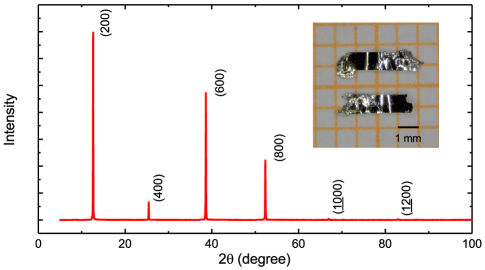
The single-crystal XRD study revealed that Ta2Pd3Te5 is of orthorhombic structure with SG (No. 62). The lattice parameters of Ta2Pd3Te5 are = 13.9531(6) Å, = 3.7038(2) Å and = 18.5991(8) Å. The detailed crystallographic parameters are summarized in Table S1. Fig. S1 shows the XRD pattern of a flat surface of Ta2Pd3Te5 single crystal, where only (00) peaks are detected. A photograph of a typical Ta2Pd3Te5 crystal is shown in the inset of Fig. S1, and the back square of mm indicates the size of the crystal. Fig. S2 shows the crystal structure of Ta2Pd3Te5 in our measurements.
| Site | ||||||
|---|---|---|---|---|---|---|
| Ta1 | 4 | 0.24318 | 0.75000 | 0.33301 | 1.000 | 0.010 |
| Ta2 | 4 | 0.25092 | 0.25000 | 0.08293 | 1.000 | 0.010 |
| Te1 | 4 | 0.13221 | 0.75000 | 0.45953 | 1.000 | 0.013 |
| Te2 | 4 | 0.40024 | 0.25000 | 0.55902 | 1.000 | 0.012 |
| Te3 | 4 | 0.38685 | -0.25000 | 0.13913 | 1.000 | 0.012 |
| Te4 | 4 | 0.39487 | 0.25000 | 0.35369 | 1.000 | 0.012 |
| Te5 | 4 | 0.39464 | -0.25000 | 0.77984 | 1.000 | 0.012 |
| Pd1 | 4 | 0.32146 | 0.25000 | 0.68820 | 1.000 | 0.014 |
| Pd2 | 4 | 0.26901 | 0.25000 | 0.45802 | 1.000 | 0.013 |
| Pd3 | 4 | 0.30827 | 0.25000 | 0.22723 | 1.000 | 0.013 |
.2 Electronic band structures and band topology of layered vdW compounds TaTe5
The bulk TaTe5 is a layered vdW material (i.e., TaTe5 layers stacking in the [100] direction) Tremel (1991). The PBE+SOC band structures for Ta2Ni3Te5 and Ta2Pd3Te5 are given in Fig. S3. As each unit cell consists two layers, four symmetry indicates () are computed to be 0. These symmetry indicates are also zero for the bulk Ta2Ni3Te5. However, the 3D bulk crystal has a mirror symmetry . So the eigen-wavefunctions can be classified into two different subspaces by the eigenvalues (i.e., ), where the Chern numbers () are well defined. Thus, the mirror Chern number is defined as () in the time-reversal invariant systems. It can be calculated by the 1D Wilson loop method. The calculated WCCs for the plane shown in Figs. S4(a,b) suggest in Ta2Ni3Te5 and in Ta2Pd3Te5. The mirror Chern number for the is zero (), whose WCCs are not presented. The nontrivial mirror Chern number in Ta2Ni3Te5 indicates the band inverted feature in its 3D crystal.
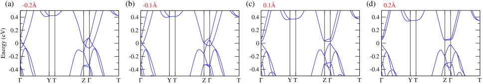
.3 The evolution of band structures when moving PdA atoms
The experimental length of the PdA-TeV bond is Å. By simply shifting the PdA atom in the -direction by , one can change the length of PdA-TeV bond.
.4 The evolution of band structures with uniaxial strains
Under uniaxial strains, the band inversion of monolayer can be tuned easily. The related band structures of monolayers Ta2Pd3Te5 (Fig. S6) and Ta2Ni3Te5 (Fig. S7) are calculated.
.5 The band structures for few layers
In the thin films, depending on the number of band inversions associated with the number of the layers, the few-layer systems show cross over between trivial and nontrivial 2D insulators according to film thickness.
