Observation and control of the weak topological insulator state in ZrTe5
A quantum spin Hall (QSH) insulator hosts topological states at the one-dimensional (1D) edge, along which backscattering by nonmagnetic impurities is strictly prohibited and dissipationless current flows KanePRL2005 ; ZhangScience2006 ; MolenkampScience2007 ; LiScience2014 ; JHScience2018 . Its 3D analogue, a “weak” topological insulator (WTI), possesses similar quasi-1D topological states confined at “side” surfaces of crystals. The enhanced confinement could provide a route for dissipationless current and better advantages for applications relative to the widely studied “strong” topological insulators (STIs). However, the topological side surface is usually not cleavable and is thus hard to observe by angle-resolved photoemission spectroscopy (ARPES), which has hindered the revealing of the electronic properties of WTIs FelserPRL2012 ; BrinkNM2013 ; WengPRX2014 ; YanPRB2014 ; ZhangPRL2016 ; PlucinskiNC2017 ; KondoNature2019 . Here, we visualize the topological surface states of the WTI candidate ZrTe5 for the first time by spin and angle-resolved photoemission spectroscopy: a quasi-1D band with spin-momentum locking was revealed on the side surface. We further demonstrate that the bulk band gap in ZrTe5 is controlled by strain to the crystal, realizing a more stabilized WTI state or an ideal Dirac semimetal (DS) state depending on the direction of the external strain. The highly directional spin-current and the tunable band gap we found in ZrTe5 will provide an excellent platform for applications.
Two of the most prominent examples of topological insulators in three dimensions are the STIs and WTIs FuPRB2007 ; FuPRB2007_2 ; HasanRMP2010 ; QiRMP2011 . Among them, STIs have been widely studied in the past decades both in theories and experiments. They host 2D spin-momentum locked Dirac cones on all surfaces, in which the perfect backscattering is prohibited, while general scattering off 180° still existsXuePRL2009 ; KomoriPRL2014 . On the other hand, WTIs host surface states only on particular side surfaces. They were thought to be weak (or not robust) since two adjacent layers in even-layer WTIs may couple with each other, leading to a topologically trivial phase. However, it was later found that the surface states of WTIs are actually robust owing to the delocalization of surface electrons RingelPRB2012 . The weak interlayer coupling in WTIs generally yields a topological surface state with quasi-1D dispersion; this could prohibit even general scattering off 180° to establish dissipationless spin current, which cannot be realized in STIs. Even with such advantages, theoretical proposals of WTIs are rare, and experimental investigations of the topological side surfaces are very challenging; layered WTI materials are inherently cleavable only on the top surface, and thus there is difficulty in preparing a large and uniform side surface for observation FelserPRL2012 ; BrinkNM2013 ; WengPRX2014 ; YanPRB2014 ; ZhangPRL2016 ; KondoNature2019 . One exception is Bi4I4, where top and side planes are both naturally cleavable KondoNature2019 . However, such crystal structures may pose obstacles in preparing a single side surface with the topological feature for applications.
The material which has been best studied from the early stage of exploring a WTI among scarce candidates is ZrTe5, which consists of a van der Waals layered structure; notably, this compound exhibits very high mobility ZhangNature2019 , thus it has been regarded as a promising platform for devices. Nonetheless, the bulk topology of ZrTe5 has not been experimentally identified to date because the observation of band structure on the side surface has not been successful so far. All the previous surface-sensitive studies were carried out on the top surface PanPRX2016 ; CrepaldiPRL2016 ; ZhouNC2017 ; ShenPRB2017 , which only confirms the lack of surface states; whether or not this material is topological, therefore, has not been determined beyond speculation. Another difficulty for this study is that ZrTe5 is in proximity to multiple topological phases, whereas this feature could bring an attractive functionality of controlling bulk topology by fine-tuning a physical parameter WengPRX2014 .
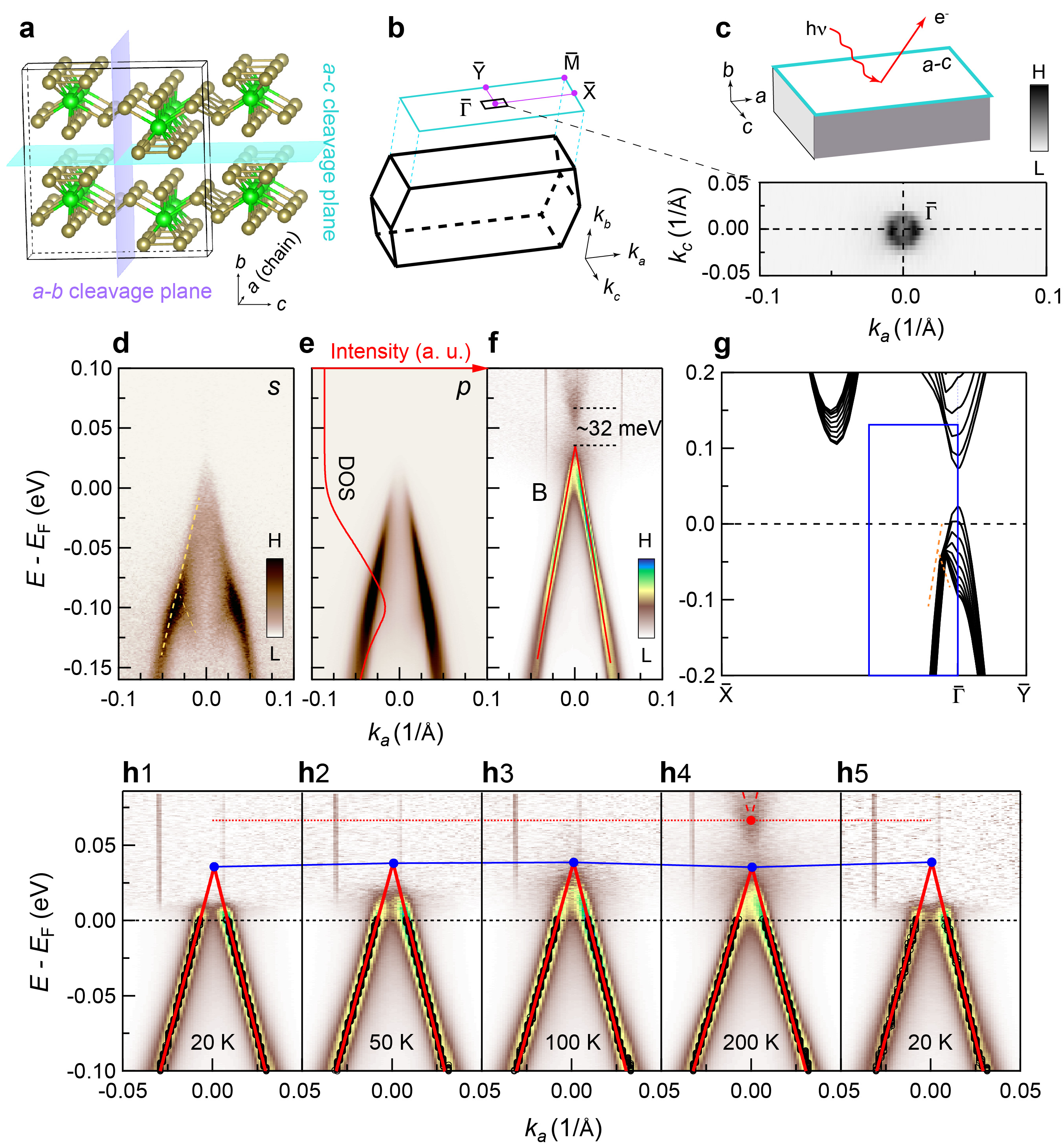
ZrTe5 has a quasi-1D crystal structure. The lattice constant along the chain direction is 4.0 Å. Except for the chain direction, the lattice constants for the other two directions are both large, as shown in Fig. 1a: The layer distance along the direction is 7.3 Å, and it is 6.9 Å along the direction FjellvagSSC1986 . As a result of the large layer distances, in principle, it should be possible to cleave both surfaces. Along the direction, the layers are stacked by van der Waals forces, and a clean surface can be easily obtained by cleavage. Instead, Te-Te bonding exists between adjacent layers along the direction, causing much more difficulty in cleaving the a-b surface. All the spectroscopic studies reported so far have been carried out on the a-c surface, which is easy to cleave VallaNP2016 ; PanPRX2016 ; LiPRL2016 ; CrepaldiPRL2016 ; ZhouNC2017 ; ShenPRB2017 .
We observed a tiny hole-type Fermi surface on the a-c surface, as shown in Fig. 1c. The band along (Fig. 1d-e) shows a cone-shape dispersion, similar to that in the previous reports except for the difference on Fermi level () VallaNP2016 ; PanPRX2016 ; ZhouNC2017 . We notice a splitting of the band in Fig. 1d at -0.1 eV, with one branch going up and the other going down, as indicated by the dashed yellows lines in Fig. 1d. Such a feature most likely originates from a average effect, and it is indeed reproduced by the first-principles slab calculations plotted in Fig. 1g along , where the series of bands come from different (); this further indicates that the slab calculations are reliable to explain the ARPES data. The measurements with -polarized light (Fig. 1e) reveal only the cone-shaped branch going up, which is thus suitable for the study of the bulk band gap.
To have a better visualization of the band structure over the whole energy range, the data in Fig. 1e is normalized by its density of states (DOS, integration of EDCs over ), as plotted in Fig. 1f (More details can be found in Supplementary Information Part II and Fig. S2). A small band gap with the size of about 32 meV is observed in the data at 200 K. Our experiments over a temperature cycle of 20K-200K-20K (Fig. 1h) have confirmed almost no change in the valence band at different temperatures; this result clearly differs from the previous reports demonstrating a large energy shift in the band with temperature PanPRX2016 ; ZhouNC2017 ; ShenPRB2017 ; XuPRL2018 . On the other hand, we have confirmed a band shift in an ARPES system with a worse vacuum level ( Torr Torr for Fig. 1h); the band shift actually occurs even for the sample kept at the same temperature (See Supplementary Information Part I and Fig. S1 for more details). These results lead us to conclude that ZrTe5 should be in a stable phase, which is not a strong topological insulator since surface states are absent in the data, but either a normal insulator or a WTI. However, with the data merely from the top surface, it is impossible to distinguish the two phases experimentally.
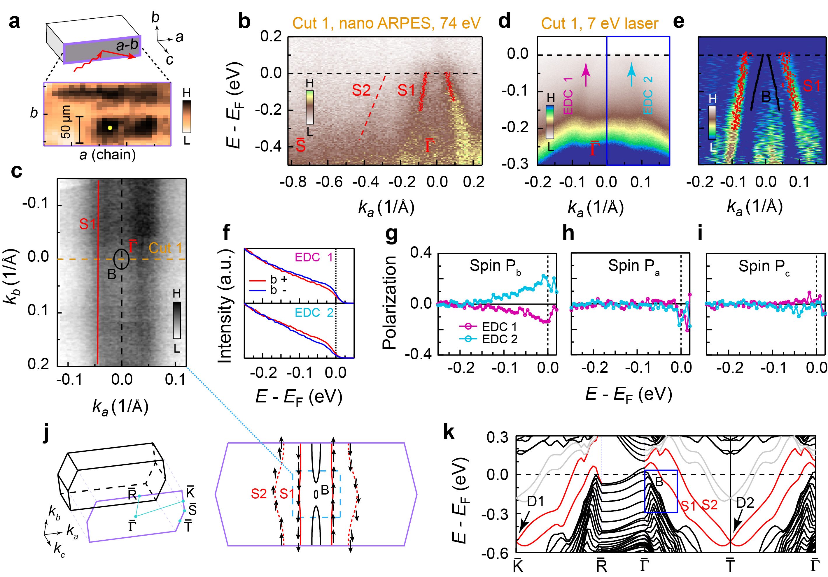
To identify the topological phase of ZrTe5, the observation of the side a-b surface is essential. We successfully cleaved the side surface with a top post and silver epoxy. The problem, however, is that the cleaved areas are very small and inhomogeneous. With a synchrotron-based nano-ARPES (spot size 1m), we took real space maps of photoemission intensity on several samples, and found that the typical dimension of cleaved areas is around or smaller than 50 m (Fig. 2a). Several positions of one cleaved area are measured and they all give the same band structure, as shown in Supplementary Information Part III and Fig. S3, indicating that the cleaved area with high photoelectron intensities is homogeneous. The selective measurements only of such a small surface area are beyond the capacity of most ARPES systems. Nevertheless, our laser-based micro-ARPES (spot size 50 m) resolved this difficulty and clearly revealed the band structure on the side a-b surface. A quasi-1D Fermi surface (S1) is exhibited in Fig. 2c by plotting ARPES intensities about the Fermi level. The band S1 shows a hole-like dispersion along (Fig. 2d-e), which has a Fermi vector much larger than that of the band B observed near on the a-c surface (Fig. 1f). The band S1 is, thus, distinct from the bulk band B located at the center of the BZ (). The bulk band B cannot be identified in ARPES data on the side a-b surface likely due to a much weaker intensity than that of the surface states. The synchrotron-based nano-ARPES measurements for Cut1 with a different photon energy (Fig. 2b) show similar result to the data obtained by laser-ARPES: Only the band S1 was clearly observed, and its dispersion is almost identical to that of the laser-ARPES data. This coincidence supports that the band S1 has a surface origin.
The spin polarization is expected for the topological surface state. To confirm this, we have used spin-resolved ARPES. In Fig. 2f, we plot EDCs (EDC 1 and EDC 2; see Fig. 2d) which are spin-resolved in the -direction; a clear spin polarization is detected (Fig. 2g). In contrast, the spin polarization is almost zero along the and directions (Fig. 2h-i). Therefore, the band S1 is spin-polarized along the -direction under the spin-momentum locking, forming a typical spin-texture of WTIs with quasi-1D dispersion (see Fig. 2j).
We also carried out the first-principles slab calculations on the side a-b surface to fully understand the ARPES data. The calculated Fermi surface (Fig. 2j) displays four sheets: two open sheets (red color) and two closed sheets (black color). By comparing these calculations with our ARPES data (Fig. 2c), we ascribe the inner open sheet to the band S1, and the closed sheets to the bulk band B. The outer open sheet (S2) was not observed with either laser-based ARPES or synchrotron-based ARPES most likely due to a small photoemission cross section. In the slab calculations, the bands S1 and S2 are localized at the surface and have spin polarization indicated by the black arrows in Fig. 2j; the spin orientation of the band S1 is consistent with our data of spin-resolved ARPES (Fig. 2f-i). The slab calculations (Fig. 2k) clearly illustrate the topological nature of the bands S1 and S2, which connect the valence and conduction bands and cross with each other at two BZ boundary points, and ; The formation of two Dirac points is a typical feature of WTIs FuPRB2007 ; FuPRB2007_2 . Although the Dirac points have not been directly detected, our data demonstrating the quasi-1D spin-momentum locking and its agreement with the first-principles calculations strongly support that the band S1 originates from the topological surface state of a WTI. The trivial bands (colored grey in Fig. 2k) crossing in the calculations are from the dangling bonds at the a-b surface, which will be removed in the calculations by proper atom absorption WangPRL2018 and do not appear in the surface Greens’ function calculations WengPRX2014 ; ZhouSR2017 insensitive to the dangling bonds. They are not intrinsic, and not observed in the experiments.
The small bulk gap ( 32 meV) we observed by ARPES indicates that the WTI state in ZrTe5 is protected only marginally from external perturbations. This is compatible with transport measurements showing semimetal behaviors in ZrTe5 VallaNP2016 ; WangPRL2015 ; XiuNC2016 ; WangPNAS2017 ; OngNP2018 . Theoretical calculations proposed that the band gap changes with external strain WengPRX2014 . Such effect could be adopted to stabilize the topological state of mater in WTI, DS or even STI state; a relevant feature has been previously reported with the data showing a strain-dependent magneto-transport possibly caused by a band gap variation ChuSA2019 . However, the signature of transport measurements is indirect, calling for the direct evidence of strain effect on the band structure by ARPES measurementsChiangNL2018 .
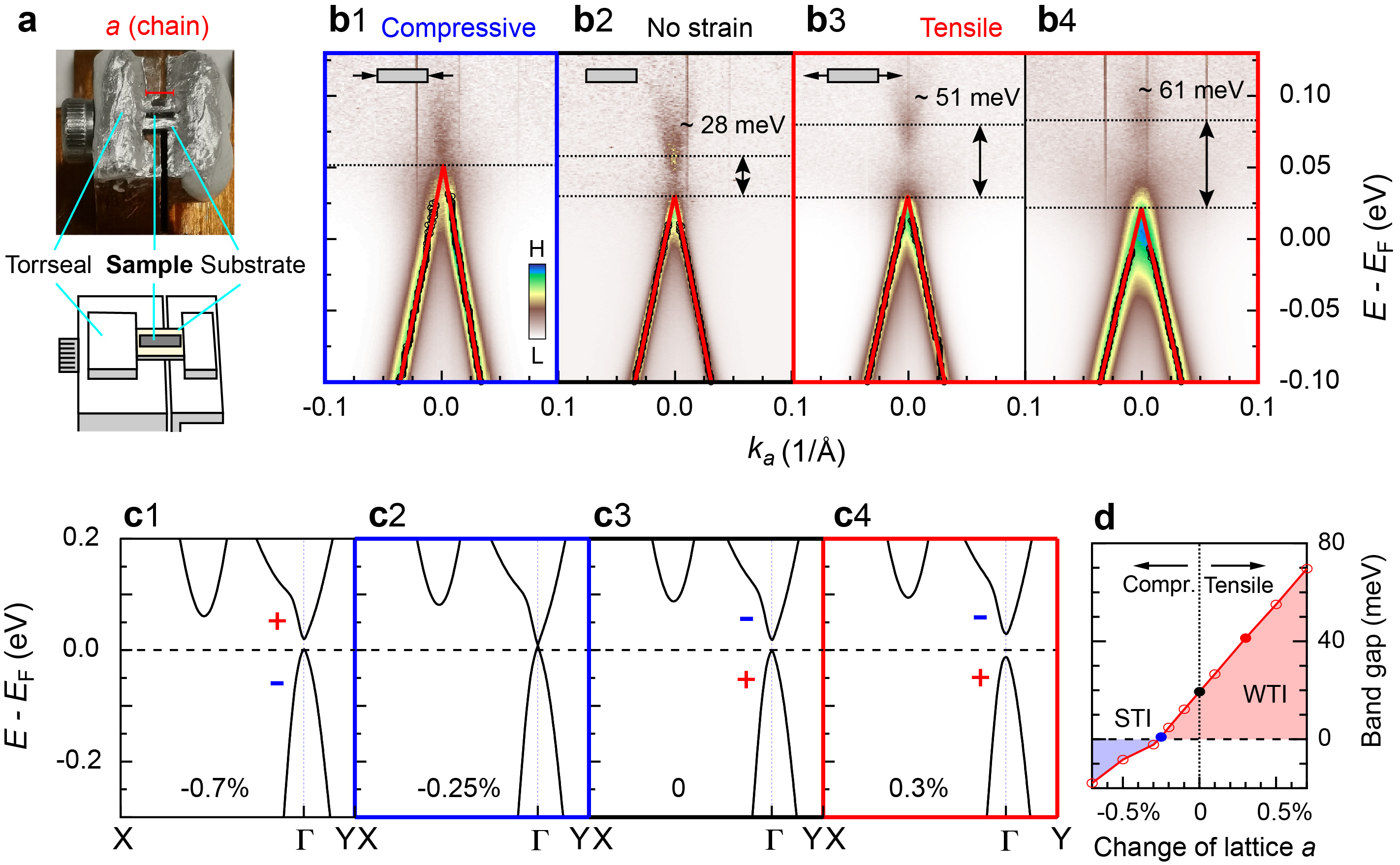
In this study, the samples are glued on Ti or BeCu substrates, to which compressive or tensile strain is applied along the chain direction of ZrTe5 (Fig. 3a; see Methods for more details). The band structures under different strain are displayed in Fig. 3b. The sample with no strain shows a band gap of 28 meV (Fig. 3b2), similar to that in Fig. 1. We have applied tensile strain to two samples, and find an increase of the band gap up to more than the double of the original value ( meV; Fig. 3b4), which makes a WTI state much more robust to external perturbations. In contrast, we could instead reduce the gap value by the compressive strain, even realizing a Dirac semimetal state with a gap no longer distinguishable (Fig. 3b1). We found that the cleaving process causes wrinkles in the sample under large compressive strain to relax the stress on the crystal lattice. It thus becomes harder to apply larger compressive strain to realize a STI state by ARPES, which requires the sample cleavage. We note, however, that cleavage is not necessary for most applications, thus a STI state could be easily reached by a compression method. In Supplement Information Part VI and Fig. S6, we further show that the band gap can be reversibly controlled by external strain.
To better understand our data, we have carried out first-principles calculations of the band structure for different lattice constants of (Fig. 3c); In ARPES, the strain was applied to the samples along the chain direction (the -axis). The calculations for compression by 0.25% (Fig. 3c2) obtain a DS state, which is consistent with the ARPES results under compressive strain in Fig. 3b1. On the other hand, the case of lattice expansion by 0.3% (Fig. 3c4) corresponds to our data under tensile strain in Fig. 3b3. Hence, we conclude that about 0.3% compression and stretch are reached in our experiments with a strain device. This is consistent with the strain values measured by X-ray diffraction on the sample and strain gauge on the substrate (See Supplementary Information Part V and Fig. S5). The band gap variation with the lattice constant is summarized in Fig. 3d, where the experimental data roughly correspond to the solid dots. The calculations further indicate that a STI state with a gap of 18 meV can be reached with 0.7% compression (Fig. 3c1), and a WTI state with a band gap about 70 meV can be reached with 0.7% stretch. Our experimental results provide the first direct evidence with ARPES on the band gap control and topological phase transition by external strain.
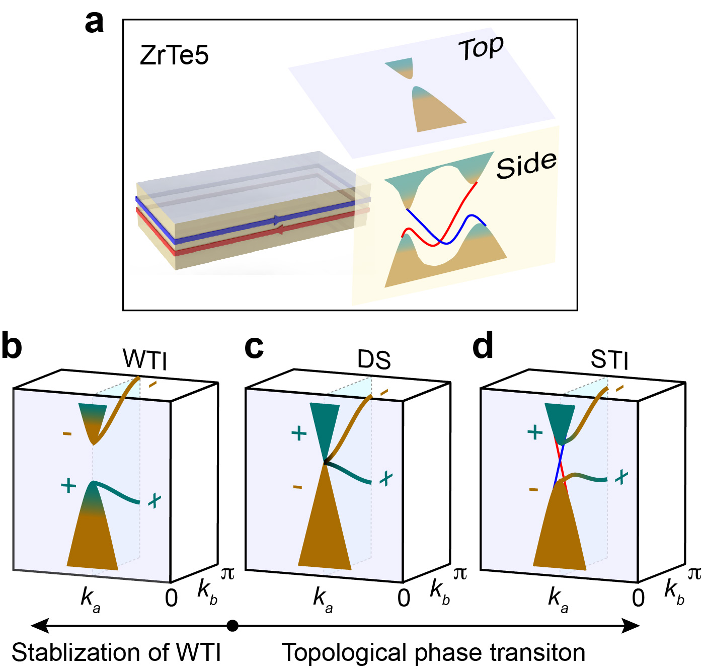
In summary, we have revealed that ZrTe5 is a WTI, as sketched in Fig. 4a, by directly observing the electronic structure not only on the top surface but also on the side surface of crystal for the first time. On the top a-c surface of ZrTe5, the band structure was confirmed to be gapped at any temperatures lower than 200K. In contrast, the side a-b surface exhibits quasi-1D surface band with spin-momentum locked texture, which illustrates the WTI nature of ZrTe5 distinct from a STI or a normal insulator. Under external strain, the band gap increases with tensile strain and decreases with compressive strain, providing a way to control the bulk gap of a WTI, or to realize a topological phase transition to a Dirac semimetal state, or even a STI state (Fig. 4b-d). A large band gap obtained by tensile strain can bring further protection of the 3D WTI state or monolayer QSH states in ZrTe5 from thermal fluctuations or other external perturbations JHScience2018 . The quasi-1D surface states yielding the highly directional dissipationless spin current and the strain-tunable bulk gap make ZrTe5 an ideal platform for 2D devices and spin engineering.
Methods
Sample growth: High-quality crystals of ZrTe5 were synthesized by the flux method with Te as the flux. High-purity elements (99.99999% Te and 99.9999% Zr) were loaded into a double-walled quartz ampoule and sealed under vacuum. The materials were first melted at 900 ℃ in a box furnace and fully rocked for 72 h to achieve a homogeneous mixture. The melt was then slowly cooled and rapidly heated between 445 and 505 ℃ for 21 days. Needle-like crystals were obtained.
ARPES: Laser-based ARPES and spin-resolved ARPES measurements were performed at the Institute for Solid State Physics, the University of Tokyo, with a laser delivering 6.994-eV photons. Photoelectrons were detected with ScientaOmicron R4000 analyzer and DA30L analyzer. The angle resolution was 0.3° (0.7°) and the overall energy resolution was set to 5 meV (30 meV) in ARPES (spin-resolved ARPES) measurements. Three-dimensional spin-polarizations of photoelectrons were detected by two VLEED-type spin detectorsYajiRSI2016 . Synchrotron-based nano-ARPES measurements were performed at the 3.2L-Spectromicroscopy beamline of the Elettra Light Source. A Schwarzschild objective was used to focus the photon beam to a spot 1m in size. The photon energy was set to 74 eV and temperature was set to around 100 K. The overall energy resolution was set to be better than 60 meV.
Band fitting: The band dispersions are extracted from MDC peaks. To avoid any complication, we simply used the position of the MDC maximums. Since the band dispersion highly resembles a cone structure, we used the following formula to fit the band structure:
where are the fitting parameters. If the computer program returns 0 or 1 for the inequality and , the above formula can be rewritten in one line:
Since the band dispersion may not be perfectly symmetric, two independent slopes were used for a better fitting. We note this method will underestimate the gap size, as the band top is actually curved due to the band gap opening. However, since the band gap is very small and the band dispersion resembles a cone structure to the very top, the difference should be quite small. Also we mainly compare the gap change with strain, such underestimation should not affect the comparison.
Strain device: The strain device shown in Fig. 3a has a unibody structure made of Be-Cu. There are two walls on the flat plate: a thick one (left) and a thin one (right). A substrate is fixed on the top of the two walls. By reducing or increasing the space between the two walls, we can apply compressive or tensile strain on the substrate, thus on the sample. In the device to apply compressive strain, the thick wall (left) has a through hole, while the thin wall (right) has a threaded hole. Thus by tightening the screw, the space between the two walls will be reduced, and compressive strain will be applied. In the device to apply tensile strain, the thick wall has a threaded hole, while the thin wall is blinded. Thus by the tightening the screw, the space will be enlarged, and tensile strain will be applied. Due to the limited space of the sample holder, Torr Seal is used to fix the substrate on top of the walls.
The data in Fig. 3b are all taken from one thick sample. We exfoliated this thick sample with scotch tape and got different flakes. Then we mounted these different flakes to the substrates of the strain devices, and carried out the experiments. With this method, we avoided the problem that different samples may have slightly different bulk band gap.
DFT calculations: Our calculations have been performed with the projector augmented wave method implemented in Vienna ab initio simulation package Kresse1996 ; KressePRB1996 . Generalized gradient approximation of Perdew-Burke-Ernzerhof type is used PerdewPRL1996 . The k-point sampling grids are set to 13137 and 771 for ZrTe5 bulk and ZrTe5 slab, respectively. Spin orbital coupling (SOC) is included in the calculations. Considering the fact that ZrTe5 is a strong topological insulator WengPRX2014 when the experimental lattice constants FjellvagSSC1986 are used, we take a slightly increased interlayer distance (0.25 Å) to mimic the weak topological insulator phase, which is consistent with our experimental observations. The ionic positions are relaxed until force on each ion is less than 0.01 eV/Å.
Data availability The data that support the findings of this study are available from the corresponding authors upon reasonable request.
-
Acknowledgements
We acknowledge X.X. Wu and Y.M. Li for useful discussions. P. Zhang is an International Research Fellow of the Japan Society for the Promotion of Science. This work was supported by MEXT Quantum Leap Flagship Program (MEXT Q-LEAP, Grant No. JPMXS0118068681) and by the JSPS KAKENHI (Grants No. JP18H01165, JP19H02683, JP19F19030, and JP19H00651). Work at Brookhaven National Laboratory was supported by the U.S. Department of Energy, Office of Science, Office of Basic Energy Sciences, under Contract No. DOE SC0012704.
-
Competing Interests
The authors declare that they have no competing financial interests.
-
Correspondence
Correspondence and request for materials should be addressed to P.Z. or T.K. (emails: zhangpeng@issp.u-tokyo.ac.jp, kondo1215@issp.u-tokyo.ac.jp)
-
Author contributions
P.Z. did the ARPES measurements and analyzed the data with help from R.N., K.Kuroda., C.L., K.Kawaguchi, K.Y., A.H., M.L., V.K., A.G., A.B. and S.S.. S.N. and H.W. did the theory calculations. Q.L. and G.D.G. synthesized the samples. All authors discussed the paper. P.Z. and T.K. wrote the manuscript and supervised the project.
References
- (1) Kane, C. L. & Mele, E. J. Quantum Spin Hall Effect in Graphene. Phys. Rev. Lett. 95, 226801 (2005).
- (2) Bernevig, B. A., Hughes, T. L. & Zhang, S.-C. Quantum Spin Hall Effect and Topological Phase Transition in HgTe Quantum Wells. Science 314, 1757 (2006).
- (3) Konig, M. et al. Quantum Spin Hall Insulator State in HgTe Quantum Wells. Science 318, 766 (2007).
- (4) Qian, X., Liu, J., Fu, L. & Li, J. Quantum spin Hall effect in two-dimensional transition metal dichalcogenides. Science 346, 1344 (2014).
- (5) Wu, S. et al. Observation of the quantum spin Hall effect up to 100 kelvin in a monolayer crystal. Science 359, 76 (2018).
- (6) Yan, B., Müchler, L. & Felser, C. Prediction of Weak Topological Insulators in Layered Semiconductors. Phys. Rev. Lett. 109, 114 (2012).
- (7) Rasche, B. et al. Stacked topological insulator built from bismuth-based graphene sheet analogues. Nat. Mater. 12, 422 (2013).
- (8) Weng, H., Dai, X. & Fang, Z. Transition-Metal Pentatelluride ZrTe5 and HfTe5: A Paradigm for Large-Gap Quantum Spin Hall Insulators. Phys. Rev. X 4, 011002 (2014).
- (9) Tang, P. et al. Weak topological insulators induced by the interlayer coupling: A first-principles study of stacked Bi2TeI. Phys. Rev. B 89, 041409 (2014).
- (10) Liu, C.-C., Zhou, J.-J., Yao, Y. & Zhang, F. Weak Topological Insulators and Composite Weyl Semimetals: -Bi4X4 (X = Br, I). Phys. Rev. Lett. 116, 014006 (2016).
- (11) Eschbach, M. et al. Bi1Te1 is a dual topological insulator. Nat. Commun. 8, 3045 (2017).
- (12) Noguchi, R. et al. A weak topological insulator state in quasi-one-dimensional bismuth iodide. Nature 566, 518 (2019).
- (13) Fu, L. & Kane, C. L. Topological insulators with inversion symmetry. Phys. Rev. B 76, 045302 (2007).
- (14) Fu, L., Kane, C. L. & Mele, E. J. Topological Insulators in Three Dimensions. Phys. Rev. Lett. 98, 106803 (2007).
- (15) Hasan, M. Z. & Kane, C. L. Colloquium: Topological insulators. Rev. Mod. Phys. 82, 3045 (2010).
- (16) Qi, X.-L. & Zhang, S.-C. Topological insulators and superconductors. Rev. Mod. Phys. 83, 1057 (2011).
- (17) Zhang, T. et al. Experimental Demonstration of Topological Surface States Protected by Time-Reversal Symmetry. Phys. Rev. Lett. 103, 266803 (2009).
- (18) Kim, S. et al. Robust Protection from Backscattering in the Topological Insulator Bi1.5Sb0.5Te1.7Se1.3. Phys. Rev. Lett. 112, 136802 (2014).
- (19) Ringel, Z., Kraus, Y. E. & Stern, A. Strong side of weak topological insulators. Phys. Rev. B 86, 467 (2012).
- (20) Tang, F. et al. Three-dimensional quantum Hall effect and metal-insulator transition in ZrTe5. Nature 569, 537 (2019).
- (21) Wu, R. et al. Evidence for Topological Edge States in a Large Energy Gap near the Step Edges on the Surface of ZrTe5. Phys. Rev. X 6, 021017 (2016).
- (22) Manzoni, G. et al. Evidence for a Strong Topological Insulator Phase in ZrTe5. Phys. Rev. Lett. 117, 237601 (2016).
- (23) Zhang, Y. et al. Electronic evidence of temperature-induced Lifshitz transition and topological nature in ZrTe5. Nat. Commun. 8, 2367 (2017).
- (24) Xiong, H. et al. Three-dimensional nature of the band structure of ZrTe5 measured by high-momentum-resolution photoemission spectroscopy. Phys. Rev. B 95, 195119 (2017).
- (25) Zhang, P. et al. A precise method for visualizing dispersive features in image plots. Rev. Sci. Instrum. 82, 043712 (2011).
- (26) Fan, Z., Liang, Q.-F., Chen, Y. B., Yao, S.-H. & Zhou, J. Transition between strong and weak topological insulator in ZrTe5 and HfTe5. Sci. Rep. 7, 45667 (2017).
- (27) Fjellvåg, H. & Kjekshus, A. Structural properties of ZrTe5 and HfTe5 as seen by powder diffraction. Solid State Commun. 60, 91 (1986).
- (28) Li, Q. et al. Chiral magnetic effect in ZrTe5. Nat. Phys. 12, 550 (2016).
- (29) Li, X.-B. et al. Experimental Observation of Topological Edge States at the Surface Step Edge of the Topological Insulator ZrTe5. Phys. Rev. Lett. 116, 176803 (2016).
- (30) Xu, B. et al. Temperature-Driven Topological Phase Transition and Intermediate Dirac Semimetal Phase in ZrTe5. Phys. Rev. Lett. 121, 187401 (2018).
- (31) Wang, J.-T., Nie, S., Weng, H., Kawazoe, Y. & Chen, C. Topological Nodal-Net Semimetal in a Graphene Network Structure. Phys. Rev. Lett. 120, 026402 (2018).
- (32) Chen, R. et al. Magnetoinfrared Spectroscopy of Landau Levels and Zeeman Splitting of Three-Dimensional Massless Dirac Fermions in ZrTe5. Phys. Rev. Lett. 115, 3786 (2015).
- (33) Liu, Y. et al. Zeeman splitting and dynamical mass generation in Dirac semimetal ZrTe5. Nat. Commun. 7, 2935 (2016).
- (34) Chen, Z.-G. et al. Spectroscopic evidence for bulk-band inversion and three-dimensional massive Dirac fermions in ZrTe5. Proc. Natl. Acad. Sci. U.S.A. 114, 816 (2017).
- (35) Liang, T. et al. Anomalous Hall effect in ZrTe5. Nat. Phys. 14, 451 (2018).
- (36) Mutch, J. et al. Evidence for a strain-tuned topological phase transition in ZrTe5. Sci. Adv. 5, eaav9771 (2019).
- (37) Flötotto, D. et al. In Situ Strain Tuning of the Dirac Surface States in Bi2Se3 Films. Nano Lett. 18, 5628 (2018).
- (38) Yaji, K. et al. High-resolution three-dimensional spin- and angle-resolved photoelectron spectrometer using vacuum ultraviolet laser light. Rev. Sci. Instrum. 87, 053111 (2016).
- (39) Kresse, G. & Furthmüller, J. Efficiency of ab-initio total energy calculations for metals and semiconductors using a plane-wave basis set. Comput. Mater. Sci. 6, 15 (1996).
- (40) Kresse, G. & Furthmüller, J. Efficient iterative schemes for ab initio total-energy calculations using a plane-wave basis set. Phys. Rev. B 54, 11169 (1996).
- (41) Perdew, J. P., Burke, K. & Ernzerhof, M. Generalized Gradient Approximation Made Simple. Phys. Rev. Lett. 77, 3865 (1996).