The Simons Observatory: Magnetic Sensitivity Measurements of Microwave SQUID Multiplexers
Abstract
The Simons Observatory (SO) will be a cosmic microwave background (CMB) survey experiment with three small-aperture telescopes and one large-aperture telescope, which will observe from the Atacama Desert in Chile. In total, SO will field 70,000 transition-edge sensor (TES) bolometers in six spectral bands centered between 27 and 280 GHz in order to achieve the sensitivity necessary to measure or constrain numerous cosmological quantities. The SO Universal Focal Plane Modules (UFMs) each contain a 150 mm diameter TES detector array, horn or lenslet optical coupling, cold readout components, and magnetic shielding. SO will use a microwave SQUID multiplexing (MUX) readout at an initial multiplexing factor of 1000; the cold (100 mK) readout components are packaged in a MUX readout module, which is part of the UFM, and can also be characterized independently. The 100 mK stage TES bolometer arrays and microwave SQUIDs are sensitive to magnetic fields, and their measured response will vary with the degree to which they are magnetically shielded. We present measurements of the magnetic pickup of test microwave SQUID multiplexers as a study of various shielding configurations for the Simons Observatory. We discuss how these measurements motivated the material choice and design of the UFM magnetic shielding.
Index Terms:
SQUIDs, Microwave Multiplexing, Supercondcuting Detectors, Magnetic Field DependenceI Introduction
Current and future cosmic microwave background (CMB) experiments rely on superconducting detectors and readout systems which are sensitive to magnetic fields. Experiments like the Simons Observatory [1], an array of new CMB telescopes to be located at 5200 m elevation on Cerro Toco in Chile, near the Atacama Cosmology Telescope (ACT) [2], CLASS [3], and the Simons Array [4], use these devices for precision measurements of the microwave sky. CMB map artifacts introduced from devices improperly shielded from scan-synchronous pickup of Earth’s magnetic field, radiating half-wave plates, magnetic components inside of cryostats, and other sources could be difficult to remove and jeopardize science goals.
SO’s 70,000 TES bolometers covering 27–280 GHz will be read out using MUX (Microwave SQUID Multiplexing) SQUIDs at an initial multiplexing factor of 1000. The densely packed 100 mK readout components will be packaged in a MUX module within a Universal Focal Plane Module (UFM), which also houses a TES array, optical coupling, and magnetic shielding [5]. Each UFM will contain 1800 MUX resonators in the 4–8 GHz band, each coupled to a dissipationless radio-frequency superconducting quantum interference device (RF-SQUID), which is in turn inductively coupled to a TES, and read out using a single pair of coaxial cables [6]. The resonators and SQUIDs for SO are developed by NIST (National Institute of Standards and Technology) [7].
The behavior of TESes and SQUIDs under the effect of magnetic fields is not well understood. Theoretical models of the superconducting phase transition of TES bolometers are not sufficiently mature to predict the response to magnetic fields, and the response of SQUID gradiometers changes with each design iteration and is difficult to simulate [8, 9]. Laboratory measurements of superconducting device magnetic field sensitivity provide valuable data on device response and magnetic shielding requirements, as well as checks on models and simulations. Previous measurements of MoCu and AlMn TES, TDM SQUIDs, and µMUX SQUIDs have provided comparative estimates of magnetic sensitivities and motivated shielding factors for upcoming experiments that are consistent with shielding factors currently in the field [10].
II Experimental Setup
II-A 512 Box MUX SQUID Measurements
The readout testing was performed using 512 MUX resonators and RF-SQUIDs on eight chips installed in the test package referred to as the “512 box.” The NIST MUX chips were of microwave SQUID design uMUX100k v1.0, wafer 1, and covered 4–8 GHz. While the MUX resonators and RF-SQUIDs may both be sensitive to magnetic fields [11], we cannot yet distinguish between the components’ behaviors, and thus refer to the magnetic pickup of each combined channel.
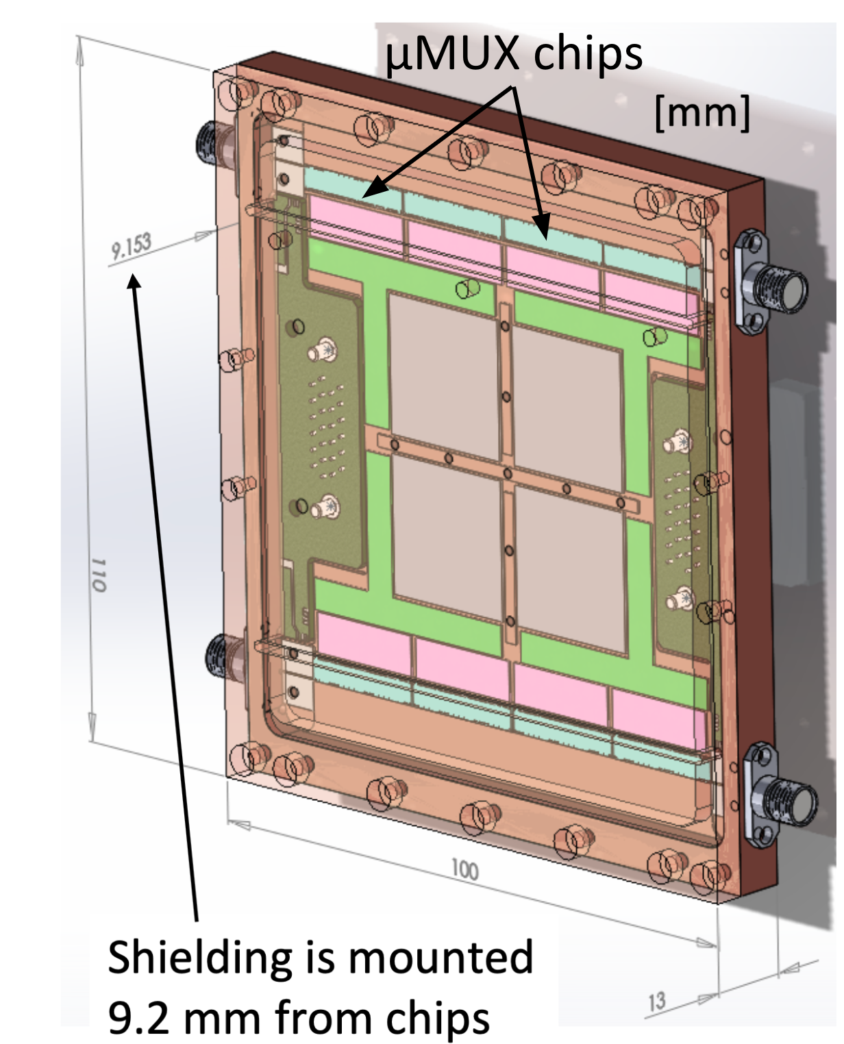
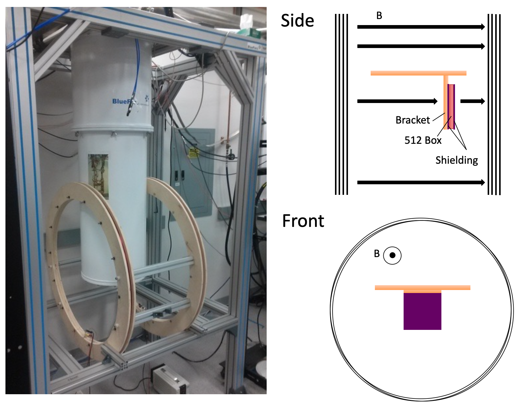
The 512 box (Fig. 1) was mounted to the cold stage of a Bluefors dilution refrigerator (DR) and cooled to 100 mK (Fig. 2). Any shielding material tested was placed on one or both sides of the test packaging, 9.2 mm from the chips. Any single layer of shielding material was mounted to the side of the 512 box shown in Fig. 1, while sandwiches of material included a layer alongside the back side in Fig. 1.
An external room temperature mu-metal magnetic shield was placed over the DR while the test chips were cooled to avoid trapping magnetic flux in the chips which would degrade their performance. Once at base temperature, this shield was removed, and a set of Helmholtz coils were positioned outside of the vacuum shell of the DR to apply constant DC magnetic fields perpendicular to the plane of the chips (Fig. 2). Fields were not applied parallel to the plane of the chips because they would not couple to the SQUIDs. No additional magnetic shielding beyond the test pieces near the chips was included.
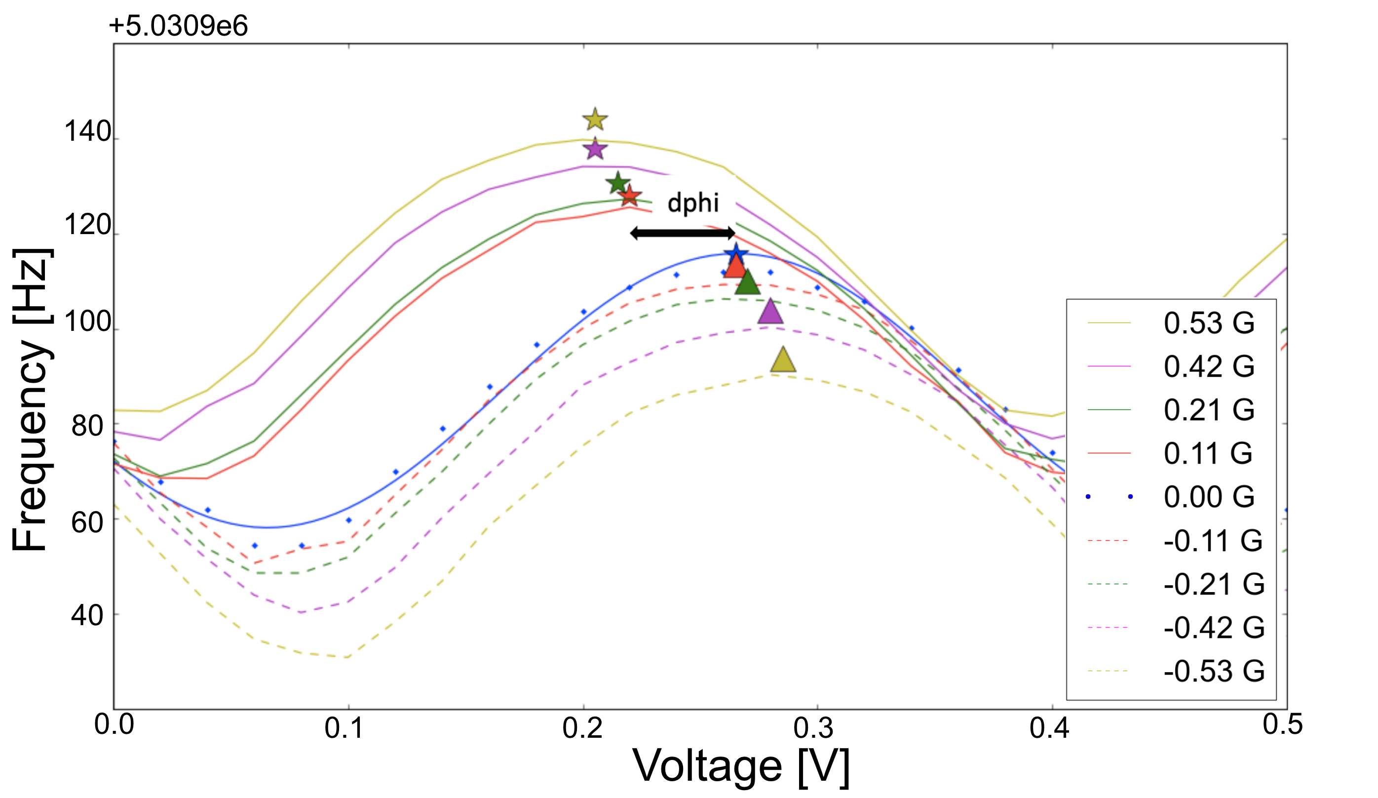
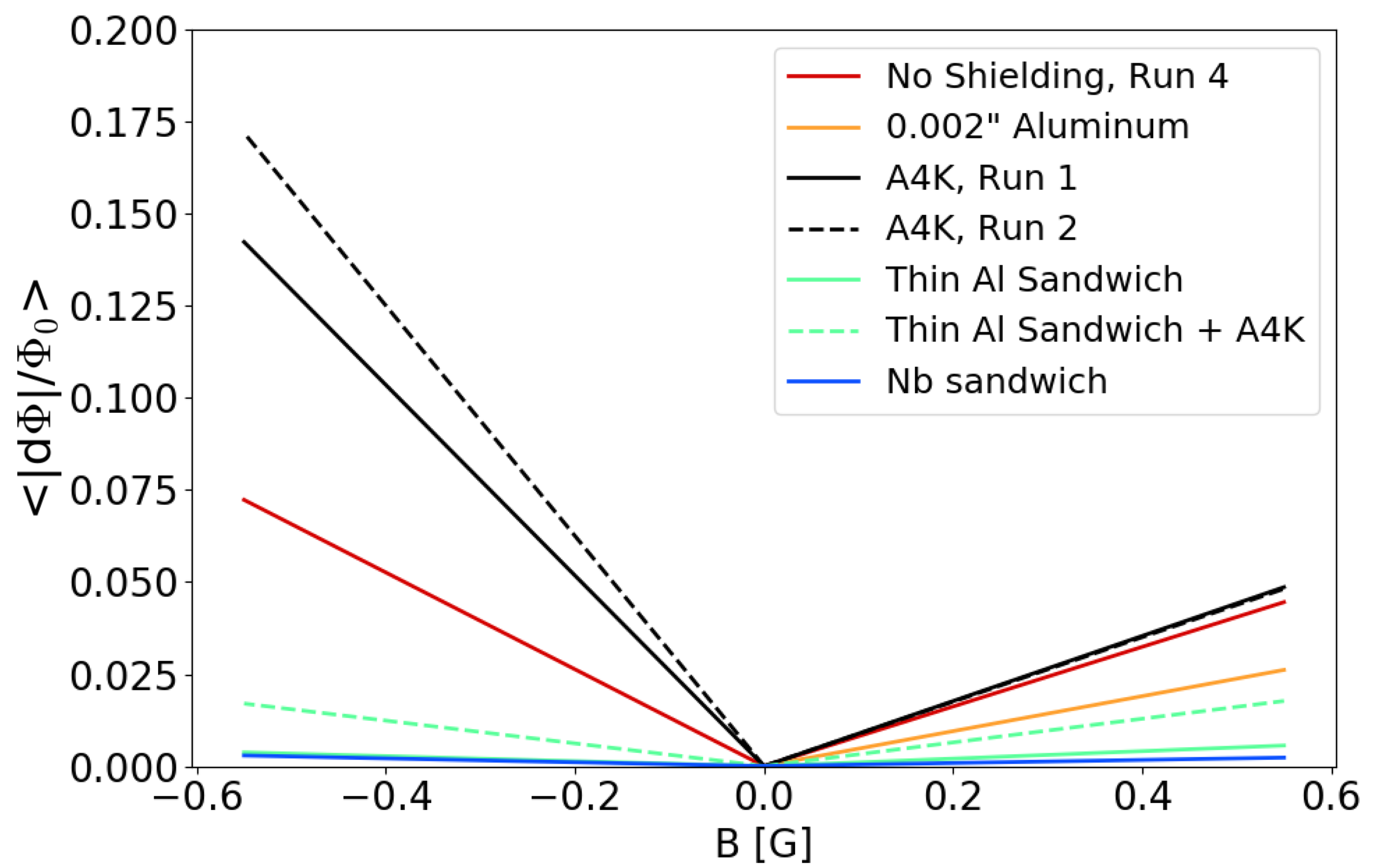
87 channels were chosen for analysis, evenly spaced across the 4–8 GHz frequency range. For each data taking run, the same channels were selected for data taking (as chosen by the closest resonance frequency match). At each applied field value, a vector network analyzer (VNA) traced f- curves for the chosen channels as the flux through the SQUID (, controlled by voltage applied) was ramped from 0 to 0.5 V in discrete steps of 0.02 V and the minimum frequency of the channel (f) was recorded. Seeking only to measure the phase offsets in , a simple sinusoid was fit to the resulting f- curves, where one period is , the magnetic flux quantum, in this case 0.39 V. The phase offsets of the sinusoid fits from peak-to-peak shifts (d/) were recorded for each SQUID (Fig. 3). The offsets from Earth’s magnetic field and the zero-flux phase are accounted for by subtracting the zero applied field d/ from all the data points for each channel, such that d/ for 0 G applied field. The absolute value of these responses is taken so that one linear fit may be performed to the positive and negative shifts. The best fit sensitivity in /G for the tested resonances was estimated by fitting a line (, where /G) to the average absolute value of the f- curve phase shifts as a function of applied magnetic fields.
II-B Magnetic Field Application
Upon reaching base temperature, the external mu-metal magnetic shield around the DR was removed, and the Helmholtz coils were installed. The highest field value tested (0.525 G) was applied for approximately one minute, and then removed. DC fields were then applied starting at 0 G for a given polarity, and stepped from 0 to 0.525 G in steps of 0.105 G. At each DC field value, f- curves for each of the resonances were obtained. Fields were applied by setting a power supply to a given current value (i.e. were set suddenly and not ramped up slowly). The field polarity was then reversed, and data were again taken starting from low to high applied field. The field polarities were not tracked between cooldowns, and small relative asymmetries between the two polarities are expected from Earth’s magnetic field.
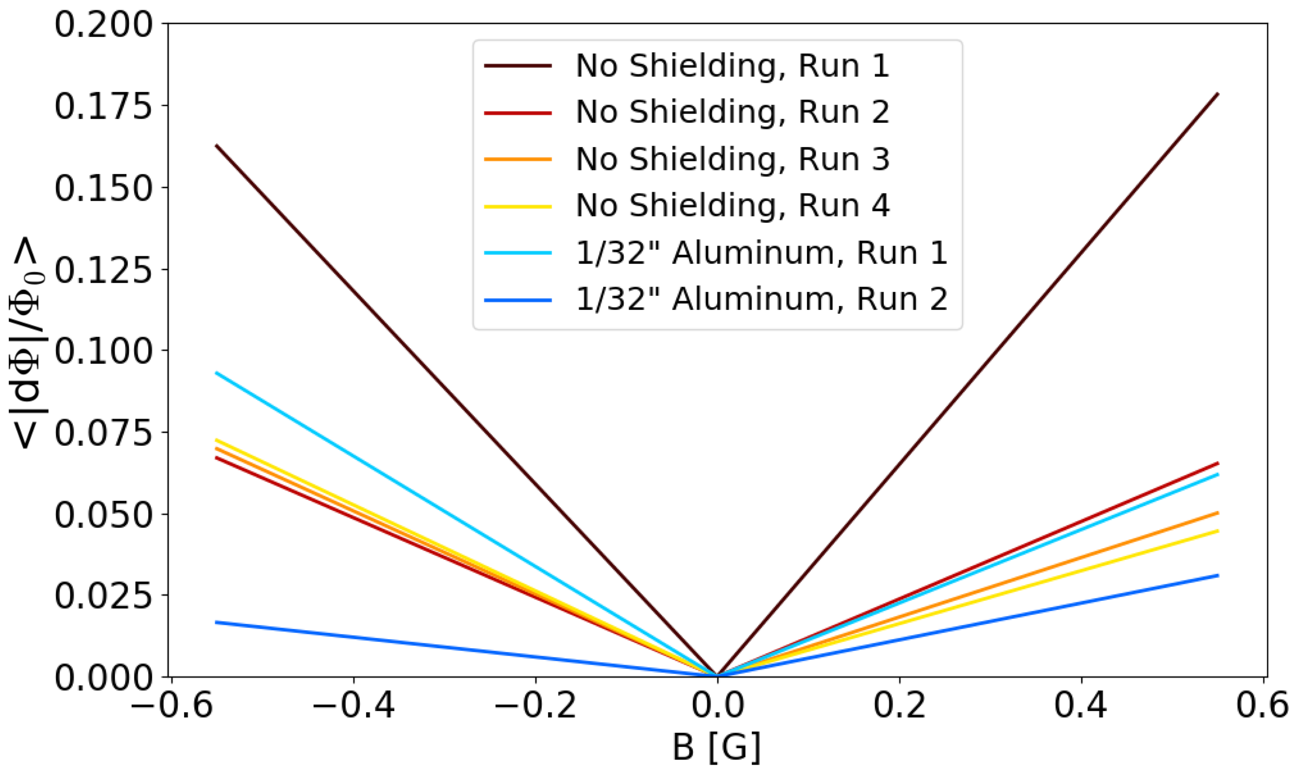
We found that exposing the chips to the highest value of applied field (0.525 G) had the effect of “settling” the channels such that their measured sensitivity was lower after this exposure as compared to before. This applied field value is larger than the component of Earth’s magnetic field running perpendicular to the surface of the chips, which is estimated to be 0.05 G. This meant that removing the external magnetic shield and taking measurements starting at 0 G to 0.525 G yields a higher pickup estimate than subsequent repeated set of identical measurements (Fig. 4). This led us to adopt the approach applying the maximum field value (0.525 G) for 1 minute before taking the data compared in Fig. 5.
No hysteresis was observed when taking data from 0 to 0.525 G in steps of 0.105 G, and then again from 0.525 to 0 G in steps of 0.105 G for the test assembly with a single piece of 0.002” Al.
II-C Shielding Materials
The magnetic shielding materials tested included two thicknesses (1/32”, 0.002”) of 6061-T6 aluminum, 0.002” thick Type 2 annealed niobium from Eagle Alloys, and a hexagonal piece (127.20 0.50 mm corner to corner, 1 mm thick) of annealed A4K from Amuneal.
III Results
Tab. I lists the sensitivity results for the tested magnetic shielding configurations. Average /Gauss sensitivities as estimated by linear fits to the average f- phase offsets for the 512 box MUX channels per applied field value are shown for each material configuration. Uncertainties listed come from the linear fits to the average data point per applied field value. A factor of sensitivity reduction from no shielding material is listed.
| Material | Sensitivity [/G]a | Reduction Factorb |
| None | 0.108 0.015 | 1.0 |
| 1/32” Al | 0.044 0.009 | 2.5 |
| 0.002” Al | 0.053 0.007 | 2.0 |
| A4K | 0.199 0.091 | 0.5 |
| 0.002” Al SWc | 0.009 0.002 | 12.0 |
| 0.002” Al SW+A4Kd | 0.033 0.005 | 3.3 |
| 0.002” Nb SWe | 0.005 0.001 | 21.6 |
| aAverage pickup of the channels for the shielding configuration. | ||
| bFactor by which sensitivity was reduced compared to no shielding. | ||
| cA sandwich of 0.002” Al. | ||
| dA sandwich of 0.002” Al + layer of A4K within the top layer of Al. | ||
| eA sandwich of 0.002” Nb. | ||
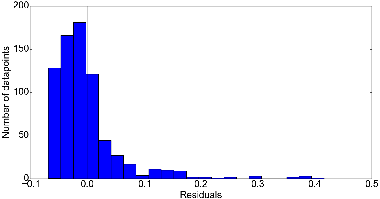
With no shielding, the 512 box MUX channels show a 0.108 0.015 /G shift as estimated using the mean linear fit. This fit is a conservative estimate of the responses, as the distribution of /G per channel was not Gaussian, but positively skewed with a lower mode (Fig. 6). The best shielding configurations tested were the sandwiches of 0.002” Al or Nb, with a layer of superconductor on either side of the MUX chips, 9.2 mm from the chip surface. These two shielding configurations reduced the shift by a factor of 12.0 or 21.6, respectively. Single layers of Al were the next most successful, providing a 2.0–2.5 factor reduction in field pickup.
The single layer of annealed A4K yielded higher pickup than no shielding, and introduced an asymmetry in sensitivity depending on field polarity. These results were repeated over multiple data-taking runs. To check for asymmetries introduced by the hexagonal shape of the A4K piece, only channels on the central 512 box chips (which were farthest from the hexagonal edges of the piece) were analyzed. The behavior was the same for these chips alone. When the piece of A4K was included inside the 0.002” sandwich of Al, the shielding was degraded by a factor of 3.6 as compared to the 0.002” sandwich of Al alone.
IV Conclusion
NIST test chip MUX resonators and RF-SQUIDs for the Simons Observatory were tested for magnetic sensitivity in a variety of magnetic shielding configurations to motivate the design of the UFM shielding. The measured unshielded channel sensitivity of 0.108 0.015 /G is in agreement with the upper bound of 0.3 /G previously placed on NIST MUX RF-SQUIDs [10]. This pickup equates to a 2 effective cross-section, or one part in of the 40,000 SQUID area, and is due to imperfect gradiometry, metal symmetry, and uniformity of applied field. Because Earth’s field can produce a magnetic flux quantum through just a 40 area, and the SQUIDs are much larger, gradiometry and magnetic shielding must be combined to provide sufficient insensitivity to Earth’s field and other sources while scanning and observing. Layers of superconducting materials 6061-T6 Al and Nb reduce the measured pickup by a factor of 2.0-21.6. This behavior agrees with general expectations as both Type I and II superconductors respond to applied magnetic fields by setting up electric surface currents which cancel out these fields. It is notable that single layers of superconductors provided 5–11 times less shielding than sandwiches of superconductors.
The presence of A4K degraded the shielding performance of an Al sandwich by a factor of 4, and increased the sensitivity of the MUX SQUIDs when compared to no shielding at all. The presence of A4K also introduced a large field polarity asymmetry. This motivated the departure from including A4K in the SO UFM packages.
Instead of canceling out applied magnetic fields like superconductors, A4K redirects them. The details of an A4K shielding geometry may thus have profound effects on the material’s shielding ability: single flat layers of A4K may not behave like cylindrical shields or boxes, acting to concentrate, distort, and amplify magnetic fields instead of redirecting and attenuating them. It can also be difficult to simulate the behavior of A4K due to numerical issues when modeling high-permeability materials like A4K directly next to zero-permeability materials like superconductors. Our measured results did not agree with our expectations from simulations using ANSYS Maxwell, which estimated that adding a single hexagonally shaped sheet of A4k to the 0.002” Al sandwich would improve, rather than degrade, the shielding performance of the sandwich by a factor of 4. The disagreement with this result from simulations highlights the importance of laboratory measurements to accurately predict the effectiveness of magnetic shielding materials and geometries.
Along the same lines, our results may not easily extend to real-world shielding designs. Current magnetic shielding tests are being conducted with a more realistic package for an SO MUX multiplexer assembly that includes a 6061-T6 Al cover with holes in it for connectors. Introducing holes in this material may degrade its shielding performance. The best performing sandwiches of continuous layers of superconductors may be difficult to implement within the UFM, so further tests are ongoing to define the UFM shielding design.
Our work has shown that it is difficult to accurately predict the performance of shielding materials in the experimental setting. To properly motivate magnetic shielding designs, laboratory or field tests of realistic materials and geometries are necessary. Such measurements may also improve future models and our understanding of simulations.
Acknowledgment
This work was supported in part by a grant from the Simons Foundation (Award No. 457687, B.K.), and by NSF Grant AST-1454881. SKC acknowledges support from the Cornell Presidential Postdoctoral Fellowship and NSF award AST-2001866. ZX is supported by the Gordon and Betty Moore Foundation.
References
- [1] www.simonsobservatory.org
- [2] J. W. Fowler et al., “Optical design of the Atacama Cosmology Telescope and the Millimeter Bolometric Array Camera,” Appl. Opt. 46, 3444 (2007), DOI:10.1364/AO.46.003444.
- [3] K. Harrington et al., “The Cosmology Large Angular Scale Surveyor,” Proc. SPIE Vol. 9914, Millimeter, Submillimeter, and Far-Infrared Detectors and Instrumentation for Astronomy VIII; 99141K (2016), DOI:10.1117/12.2233125.
- [4] K. Arnold et al., “The bolometric focal plane array of the POLARBEAR CMB experiment,” Proc. SPIE 8452, Millimeter, Submillimeter, and Far-Infrared Detectors and Instrumentation for Astronomy VI; 84521D (2012), DOI:10.1117/12.927057.
- [5] Y. Li, K. Arnold, Z. Atkins et al., “Assembly and integration process of the high-density detector array readout modules for the Simons Observatory,” J Low Temp Phys 199, 985–993 (2020), DOI:10.1007/s10909-020-02386-6.
- [6] M. Sathyanarayana Rao, M. Silva-Feaver, A. Ali et al., “Simons Observatory microwave SQUID multiplexing readout: cryogenic RF amplifier and coaxial chain design, J Low Temp Phys 199, 807–816 (2020), DOI:10.1007/s10909-020-02429-y.
- [7] B. Dober et al. “Microwave SQUID multiplexer demonstration for cosmic microwave background imagers,” Applied Physics Letters 111 (24), 243510 (2017), DOI 10.1063/1.5008527.
- [8] J. N. Ullom and D. A. Bennett, “Review of superconducting transition-edge sensors for x-ray and gamma-ray spectroscopy,” Superconductor Science and Technology, Volume 28, Issue 8, article id. 084003 (2015).
- [9] J. E. Sadleir, S. J. Smith, S. R. Bandler, J. A. Chervenak and J. R. Clem, “Longitudinal proximity effects in superconducting transition-edge sensors”, Phys. Rev. Lett. 104, 047003, (2010).
- [10] E. M. Vavagiakis, S. W. Henderson, K. Zheng et al., “Magnetic sensitivity of AlMn TESes and shielding considerations for next-generation CMB surveys,” J Low Temp Phys 193, 288–297 (2018), DOI:10.1007/s10909-018-1920-5.
- [11] D. Flanigan, B. R. Johnson et al., “Magnetic field dependence of the internal quality factor and noise performance of lumped-element kinetic inductance detectors,” Appl. Phys. Lett. 109, 143503 (2016).