Exposing the trion’s fine structure by controlling the carrier concentration in hBN-encapsulated MoS2
Abstract
Atomically thin materials, like semiconducting transition metal dichalcogenides, are highly sensitive to the environment. This opens up an opportunity to externally control their properties by changing their surroundings. In this work, high-quality van der Waals heterostructures assembled from hBN-encapsulated monolayer MoS2 are studied with the aid of photoluminescence, photoluminescence excitation, and reflectance contrast experiments. We demonstrate that carrier concentration in MoS2 monolayers, arising from charge transfer from impurities in the substrate, can be significantly tuned within one order of magnitude by the modification of the bottom hBN flake thickness. The studied structures, characterized by spectral lines approaching the narrow homogeneously broadened limit enabled observations of subtle optical and spin-valley properties of excitonic complexes. Our results allowed us to resolve three optically-active negatively charged excitons in MoS2 monolayers, which are assigned to the intravalley singlet, intervalley singlet, and intervalley triplet states.
1 Introduction
Two-dimensional (2D) layered materials remain for the past decade an object of great attention due to their physical properties. They are laterally bound by strong covalent bonds, which provide high in-plane stability. Whereas weak van der Waals (vdW) interlayer interactions allow isolating thin flakes up to single layer thickness. [1, 2] One of the most studied families of layered materials are semiconducting transition metal dichalcogenides (S-TMDs) with formula MX2 where M=Mo or W and X=S, Se or Te. As the thickness of S-TMDs approaches the atomic limit, substrate-induced effects predominate their optical and electronic behavior. [3, 4, 5, 6, 7] In particular, it has been shown that variations in morphology, thickness, and flake-substrate bonding strength on the same substrate can still have a major impact on the material properties. [8, 9, 10]
To overcome some of those substrate-related issues, attention has been directed towards the fabrication of vdW heterostructures using hexagonal boron nitride (hBN). [11, 12] The inert, flat, and uniform surface of the hBN thin flakes provides an ideal substrate for S-TMD monolayers (MLs). Their similar crystalline structure, retained by weak van der Waals interactions between individual layers, without dangling bonds on surfaces, allows for easy assembly of lattice mismatch-free structures. The hBN layers also serve as barriers preventing charge transfer from impurities in commonly used SiO2/Si substrates. [13, 14, 15]
The MoS2 MLs, like other atomically thin materials, are highly sensitive to their surroundings. It was demonstrated that employing Si or SiO2 substrates led to the quenching of the photoluminescence (PL) as well as to doping effects due to the charge transfer from the substrate to the ML. [3, 16, 17] The hBN flakes used as substrates proved to be remarkably suitable to prevent those effects. Their nearly charge-neutral nature with atomically flat surfaces provides buffer layers, which preserve intrinsic properties of ML MoS2. The hBN substrate does not contribute to the inhomogeneous broadening of the optical transitions, often caused by surface roughness. There are also no charged impurities in hBN layers, which could generate substantial disorder in the host material. [18, 19] Despite the important role the hBN layers play in preserving the MoS2 inherent characteristics, understanding the influence of the thickness of the bottom hBN flake on the properties of S-TMD MLs requires more in-depth exploration.
In this work, we conduct a systematic characterization of the optical response of the hBN-encapsulated MoS2 with varying thickness of the bottom hBN layer ranging from 4 nm to 134 nm using the PL, photoluminescence excitation (PLE), and reflectance contrast (RC) experimental techniques. We show that the intensity ratio of the emission due to neutral and charged excitons in MoS2 ML strongly depends on the bottom hBN flake thickness. We conclude that the carrier density in the MoS2 ML can be significantly controlled by adjusting the thickness of the supporting hBN layer, particularly, in the limit of few nm. The high quality of our structures, confirmed by small linewidths of the neutral exciton emission (on the level of a few meV), allows us to unveil the fine structure of negative trions in MoS2 MLs. We attribute their components to three configurations of negatively charged excitons: an intravalley singlet, an intervalley singlet, and an intervalley triplet.
2 Results
2.1 Modification of carrier concentration in MoS2 monolayers
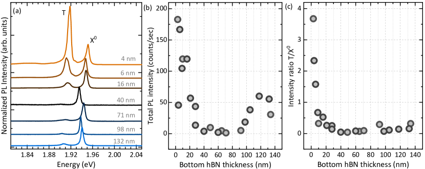
A series of samples were prepared with MoS2 MLs encapsulated in hBN flakes with different thicknesses of the bottom hBN flakes ranging from 4 nm to 134 nm. Selected PL spectra of the hBN-encapsulated MoS2 MLs measured at =5 K are shown in Fig. 1(a). As can be appreciated in the Figure, two emission lines are apparent in all the presented spectra, which is consistent with several previous works done on MoS2 MLs embedded between two hBN flakes. [18, 20, 21] Following those reports, the highest energy emission peak (X0) is attributed to the neutral exciton formed in the vicinity of the optical band gap (A exciton), while the lower-in-energy feature (T) corresponds to the recombination of a negatively charged exciton (negative trion). The sign of free carriers is determined from the fine structure of the trion apparent in the PL, PLE, and RC spectra, which is analyzed in more detail in the next Section. As it is seen in Fig. 1(b), the total PL intensity varies significantly by more than two orders of magnitude with the thickness of bottom hBN. Moreover, the presented dependence is not monotonic, the minimum of the intensities is seen for thickness of bottom hBN in the range 40 – 90 nm. This behaviour is attributed to the interference effects in the investigated dielectric stacks in which the variation of the bottom hBN layer thickness on Si substrate can be treated as an analog of the change of SiO2 thickness in commonly used SiO2/Si substrates. It was demonstrated that the X0 emission in MoS2 MLs measured at room temperature could be enhanced about 20 times by using SiO2 with thickness in the range of 192 – 328 nm. [22] The dielectric environment is also responsible for a shift in the energy of the emission lines. A similar effect can be obtained by strain. MoS2 flake is normally subjected to residual stresses resulting from the transfer procedure during sample fabrication. [23, 24] However, in our analysis we disregard these factors, as they should have no substantial impact on doping effects, excluding charge trapping or creating localized states, as their occurrence are relatively rare.
Now let us focus on the detailed analysis of the measured PL spectra. For the thinnest bottom hBN flake of 4 nm thickness, the T emission is much more intense as compared to the X0 one. When the bottom hBN flake gets thicker, the optical emission due to the neutral exciton starts to dominate the PL spectra, while the trion intensity substantially decreases. Fig. 1(c) demonstrates the intensity ratio of the X0 and T emissions as a function of hBN thickness. One can observe a decline in this ratio by two orders of magnitude from 3 to 0.03 with the hBN thickness approaching approx. 20 nm. For thicker hBN flakes the intensity ratio saturates to a roughly constant value. This behavior suggests the influence of external factors on the emission spectra and thus on the inherent properties of the studied MLs.
MoS2 crystals generally bear inherent -type doping, including the MLs discussed within this report. This characteristic is linked to abundant sulfur vacancies in the bulk crystal. [25, 26, 27, 28, 29] On the other hand, many reports show that the properties of this material vary depending on the structure in which it is used. In particular, encapsulating MoS2 significantly changes the optical or electrical performance of MLs, indicating their sensitivity to some external factors that affect their intrinsic properties. [30, 31, 32]
In our analysis, we adopt the reasoning that MLs obtained from a single bulk crystal share similar properties, particularly, a comparable level of doping. This means that the observed variation in the PL response within a given series of samples can be associated with the variation of the bottom hBN flake thickness. The distinctly higher emission intensity of the T line compared to the X0 one for the thinnest lower hBN flake is a signature of the high electron concentration in these MoS2 MLs. We belive that the increased concentration stems from quantum tunneling of carriers from impurities present in SiO2/Si substrates.
As similar considerations have not been widely addressed in optical measurements, we invoke the results of electrical studies. Since hBN is an insulator with a large energy band gap, it is an excellent dielectric material that has been widely used as a building block of high-performance devices, as a tunneling barrier. [33, 34, 35, 36, 37] Even though some reports suggest that a single atomic hBN layer acts as effective isolation, [34] it is often found, that the very thin flakes do not provide efficient barriers for carriers. [14, 15]. As the transmission probability of the hBN barrier decreases exponentially with the number of atomic layers, most devices rely on the barrier of single nanometers in thickness. [36, 38, 39, 40, 41] However, the electron wave function can penetrate even larger number of layers, up to 9 nm thick. [35, 42, 43, 44]
A parallel pattern can be followed in our results, where charge carrier tunneling seems to occur for structures with bottom hBN thickness below 10 nm, as manifested by the strong trion-related emission (see Fig.1). Above this limit, the density of free carriers in the MoS2 MLs attains an inherent doping level of a natural crystal.
To provide an estimate of the carrier concentration in the investigated MLs, the extracted values of X0–T ratio, presented in Fig. 1(c), are compared with the PL results measured as a function of free electron concentration in Ref. [45]. It has been found that the electron concentration () equals about 3 1012 cm-2 in the MLs on 4 nm hBN, then decreases by about one order of magnitude for 10 nm thick bottom hBN flake. The presented approach can be adapted to other S-TMDs MLs, such as MoSe2, MoTe2, WS2, and WSe2, which gives us a useful tool to tune the carrier concentration in S-TMD MLs deposited on hBN flakes.
2.2 Fine structure of negative trions
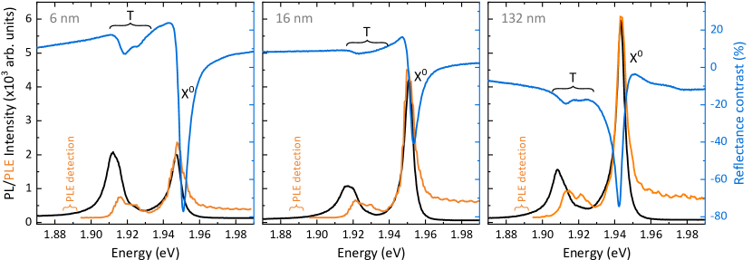
To investigate thoroughly the effect of bottom hBN thickness on both the emission and absorption processes in MoS2 MLs, we have focused our further investigations using three experimental techniques (PL, PLE, and RC) on selected samples with hBN substrate thicknesses of 6 nm, 16 nm, and 132 nm, see Fig. 2. As can be appreciated in the Figure, the presence of the X0 and T resonances are observed in all of the measured spectra. Let us turn the attention to a detailed analysis of the feature in the vicinity of the T complex. While two absorption-type resonances can be easily distinguished for the negative trions in the PLE and RC spectra, the corresponding emissions comprise up to three components. A double structure of the trion in MoS2 ML has been recently ascribed to the intravalley spin-singlet and intervalley spin-singlet negatively charged excitons for the higher and lower-energy features, respectively. [21, 46] The lowest energy resonance visible only in the PL spectra has been related to intervalley spin-triplet negatively charged exciton (see the next Section for details).
It is also worth pointing out that the interference effects in the investigated dielectric stacks affect not only the overall PL intensity (see Fig. 1), but also the lineshape of resonances observed in the RC spectra (see Fig. 2). A similar effect on the observed RC features was reported for MoS2 MLs deposited on SiO2/Si substrates. [47]
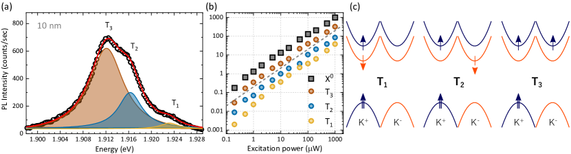
The fine structure of the negative trion, apparent in both emission and the absorption experiments, is displayed distinctly in Fig.3(a), in which a combination of three Lorentzian curves was fitted to data. The extracted energy separation between the T1 and T2 is equal to 7 meV, which is consistent with the corresponding value of around 8 meV from RC measurements. [46] The extracted T2-T3 energy separation is of the order of 4 meV. The observation of the T3 line in the PL spectrum is most surprising, as its contribution to the RC and PLE spectra is absent (see Fig. 2. To verify the origin of the T lines, the PL spectra have been measured with varying excitation power. The integrated intensities of the negative trions and the neutral exciton display a linear dependence on the excitation power, see Fig. 3(b), as is expected for excitonic features comprising a single electron-hole (-) pair. [48]
The apparent fine structure of the negative trion might seem surprising, as the theoretically predicted structure of the conduction (CB) and valence (VB) bands leads to the optical activity of the energetically lowest transition. [49] This picture however does not include the excitonic character of the optical response of S-TMD MLs. [7] It has recently been demonstrated that the excitonic ground state in MoS2 MLs encapsulated in hBN is optically inactive or dark, [50] which places this material within the family of so-called MLs. For other darkish MLs, such as WS2 and WSe2, two configurations of the negative trions, intravalley spin-singlet and intervalley spin-singlet states, were reported in the literature. [51, 52, 53, 54] It is important to mention that the small CB spin-orbit splitting in MoS2 MLs, predicted to equal about 3 meV, [49] leads to yet another effect. This is the reordering of the spin-split and spin-polarized CB subbands in the K valley occupied by an electron-hole (-) pair forming a trion. The reordering results from a difference in the effective electron mass in the subbands combined with the - interaction (see Ref. [21, 46] for details). This leads to the same arrangement of CB subbands in both the K+ and K- points of the Brillouin zone, in contrast to the opposite arrangement in the W-based MLs. [51, 52, 53, 54]. Consequently, three spin configurations of the optically-active (bright) negatively charged excitons in MoS2 MLs may be formed in the K+ valley, intravalley spin singlet (T1), intervalley spin singlet (T2), and intervalley spin-triplet (T3), see Ref. [55]. Fig. 3(c) presents schematic illustration of the discussed possible spin configurations for optically-active (bright) negative trions formed in the K+ point in the monolayer MoS2. Note that all corresponding negative trions can also be formed in the K- valley, which leads to two possible configurations of a given complex.
By comparing the measured RC, PLE, and PL spectra on the MoS2 MLs with 6 nm and 16 nm bottom hBN flakes (see Fig. 2) and the RC spectra reported in Ref. [46], we relate the highest- (T1) and middle-energy (T2) resonances to the intravalley spin-singlet and intervalley spin-singlet negative trions, respectively. The assignment of the T3 is the most difficult, as its contribution is only manifested in PL spectra and it has not been reported so far. We ascribe tentatively T3 line to the emission of the intervalley spin-triplet state of the charged exciton, see Fig. 3(c). The intervalley trion is the energetically lowest, as the two electrons occupy both valleys allowing them to reside in the energetically lowest CB. [55] The appearance of the T3 emission can be due to a photo-doping process in the PL experiment, which can explain the lack of the T3 contribution in the corresponding RC and PLE spectra. Recently, it has been demonstrated that the laser excitation may induce free electron concentration in MoS2 MLs ranging up to several times 1012 cm-2. [56] Due to the small CB spin-orbit splitting and the photo-doping processes, we assumed that the Fermi level is high enough to provide free electrons on the higher energy CB subband allowing the formation of the intervalley triplet state of the negative trion.
In order to investigate the properties of the negative trions, the helicity-resolved PL spectra were measured on the MoS2 ML on the 6 nm bottom hBN flake in magnetic fields up to 10 T oriented perpendicularly to ML’s plane (out-of-plane configuration), see Fig. 4(a). Applying an out-of-plane magnetic field yields the excitonic Zeeman effect, [57] which is apparent as splitting into two circularly polarized components of each transition. To facilitate the analysis of that evolution, we fitted these results with Lorentzian functions. The extracted transitions energies of both the and polarized components as a function of magnetic fields are summarized in Fig.4(b). As can be appreciated in the Figure, all the / features experience redshift/blueshift with increasing magnetic field. The energy evolution of the -polarized lines, can be described by the following equation:
| (1) |
where is the transition energy at zero magnetic field, denotes the -factor of the considered excitonic complex and is the Bohr magneton. Results of the fitting are shown in Fig.4(b) with solid black curves. The obtained -factor of the neutral exciton (X0) equals about -2.7. This value is consistent with previously reported -factor values for the X0 line measured in MoS2 MLs encapsulated in hBN, which stay within the range from -1.9 to -3. [18, 21, 45, 58] For the trion-related transitions: T1, T2, and T3, the corresponding -factors are equal to -3.2, -2.6, and -1.8. In spite of the clear decrease of the trion -factor with decreasing the transition energy, the found difference cannot be explained with the existing theories for excitonic -factor in S-TMD MLs and requires further theoretical investigation.
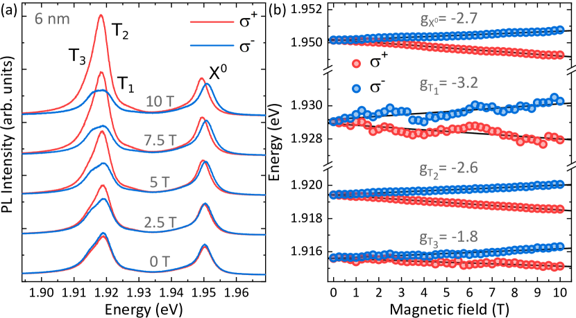
Apart from the aforementioned analysis of the magnetic-field dependence of transition energies, the applied magnetic field may also affect the emission intensities of the components. [54, 57] As can be seen in Fig. 4(a), both components of the X0 line are characterized by almost the same intensity in magnetic fields, which is characteristic for this complex in darkish MLs. [57, 7, 46] Simultaneously, all trion-related emissions are polarized in higher fields. This effect is seen distinctly for the T1 and T2 line, for which the lower/higher energy (/) component gains/loses in intensity with the increased magnetic field. The observed evolution for T1 and T2 line is analogous for observed in RC spectra (see Supplementary Materials) and was previously reported in Ref. [46]. This effect can be understood in terms of thermal distribution of free electrons between field-split states (see Refs. [46, 57] for details). In the case of the T3 line, the opposite behaviour is expected so that the magnetic field induces the gain/loss of higher/lower energy (/) component. [55] Unfortunately, the quality of results, presented in Fig. 4(a), does not allow us to unquestionably assign it. Moreover, the understanding of the magnetic-field evolution of the T3 intensity can be more complex, as the emission of this complex is observed due to the photo-doping effect. It should be also emphasized that the magnetic field dependence of trion intensities in MoS2 ML is completely different from the corresponding one observed for intravalley and intervalley negatively charged excitons in WS2 ML. [54]
3 Summary
In summary, we present a systematic study of the effect of lower hBN thickness on the optical properties of hBN encapsulated MoS2 MLs. Our results demonstrate that high electron concentration in TMD MLs usually originates from charge transfer from the substrate. The hBN flakes used as substrates act as barriers for carriers originating from those impurities. The effectiveness of such a barrier depends on its thickness. This approach can be used to manipulate the carrier concentration in the studied material. The reported investigation also allows unraveling the fine structure of the trion-related transition in the MoS2 MLs. The three optically active complexes have been attributed to an intravalley singlet, an intervalley singlet, and an intervalley triplet. The observation of the latter transition in the emission is related to the small CB spin-orbit splitting in MoS2 ML and the photo-doping processes. The effective g-factors of all trion complexes have been determined. The existence of these trion features confirms the reordering of the spin-split and spin-polarized CB subbands in the K valley, allowing the three spin configurations of the bright negatively charged excitons. Given that substrates are typically needed for most research and applications, our results are highly relevant allowing for a deeper qualitative understanding of environmentally induced changes on intrinsic properties of S-TMDs MLs.
Sample fabrication, experimental details and reflectance contrast results in magnetic field can be found in Supplementary Material.
Acknowledgements
The work has been supported by the National Science Centre, Poland (grant no. 2017/27/B/ST3/00205, 2017/27/N/ST3/01612, 2018/31/B/ST3/02111), EU Graphene Flagship project (no.785219), the ATOMOPTO project (TEAM programme of the Foundation for Polish Science, co-financed by the EU within the ERD-Fund), and the CNRS via IRP "2DM" project. K. W. and T. T. acknowledge support from the Elemental Strategy Initiative conducted by the MEXT, Japan, (grant no. JPMXP0112101001), JSPS KAKENHI (grant no. JP20H00354), and the CREST (JPMJCR15F3), JST.
References
- [1] Ming-Yang Li, Chang-Hsiao Chen, Yumeng Shi, and Lain-Jong Li. Heterostructures based on two-dimensional layered materials and their potential applications. Materials Today, 19(6):322–335, jul 2016.
- [2] A. K. Geim and I. V. Grigorieva. Van der Waals heterostructures. Nature, 499(7459):419–425, jul 2013.
- [3] Yao Guo, Xianlong Wei, Jiapei Shu, Bo Liu, Jianbo Yin, Changrong Guan, Yuxiang Han, Song Gao, and Qing Chen. Charge trapping at the MoS2-SiO2 interface and its effects on the characteristics of MoS2 metal-oxide-semiconductor field effect transistors. Applied Physics Letters, 106(10):103109, mar 2015.
- [4] Youngho Kang and Seungwu Han. An origin of unintentional doping in transition metal dichalcogenides: the role of hydrogen impurities. Nanoscale, 9(12):4265–4271, 2017.
- [5] Sven Borghardt, Jhih-Sian Tu, Florian Winkler, Jürgen Schubert, Willi Zander, Kristjan Leosson, and Beata E. Kardynał. Engineering of optical and electronic band gaps in transition metal dichalcogenide monolayers through external dielectric screening. Phys. Rev. Materials, 1:054001, Oct 2017.
- [6] Subhamoy Ghatak, Atindra Nath Pal, and Arindam Ghosh. Nature of electronic states in atomically thin MoS2 field-effect transistors. ACS Nano, 5(10):7707–7712, sep 2011.
- [7] M. R. Molas, A. O. Slobodeniuk, K. Nogajewski, M. Bartos, Ł. Bala, A. Babiński, K. Watanabe, T. Taniguchi, C. Faugeras, and M. Potemski. Energy spectrum of two-dimensional excitons in a nonuniform dielectric medium. Phys. Rev. Lett., 123:136801, Sep 2019.
- [8] D. Sercombe, S. Schwarz, O. Del Pozo-Zamudio, F. Liu, B. J. Robinson, E. A. Chekhovich, I. I. Tartakovskii, O. Kolosov, and A. I. Tartakovskii. Optical investigation of the natural electron doping in thin MoS2 films deposited on dielectric substrates. Scientific Reports, 3(1):3489, dec 2013.
- [9] Qing Hua Wang, Zhong Jin, Ki Kang Kim, Andrew J. Hilmer, Geraldine L. C. Paulus, Chih-Jen Shih, Moon-Ho Ham, Javier D. Sanchez-Yamagishi, Kenji Watanabe, Takashi Taniguchi, Jing Kong, Pablo Jarillo-Herrero, and Michael S. Strano. Understanding and controlling the substrate effect on graphene electron-transfer chemistry via reactivity imprint lithography. Nature Chemistry, 4(9):724–732, aug 2012.
- [10] M. Grzeszczyk, M. R. Molas, M. Bartoš, K. Nogajewski, M. Potemski, and A. Babiński. Breathing modes in few-layer MoTe2 activated by h-BN encapsulation. Applied Physics Letters, 116(19):191601, may 2020.
- [11] F. Withers, O. Del Pozo-Zamudio, A. Mishchenko, A. P. Rooney, A. Gholinia, K. Watanabe, T. Taniguchi, S. J. Haigh, A. K. Geim, A. I. Tartakovskii, and K. S. Novoselov. Light-emitting diodes by band-structure engineering in van der Waals heterostructures. Nature Materials, 14(3):301–306, feb 2015.
- [12] Johannes Binder, Freddie Withers, Maciej R. Molas, Clement Faugeras, Karol Nogajewski, Kenji Watanabe, Takashi Taniguchi, Aleksey Kozikov, Andre K. Geim, Kostya S. Novoselov, and Marek Potemski. Sub-bandgap voltage electroluminescence and magneto-oscillations in a WSe2 light-emitting van der Waals heterostructure. Nano Letters, 17(3):1425–1430, feb 2017.
- [13] KS Novoselov, o A Mishchenko, o A Carvalho, and AH Castro Neto. 2D materials and van der waals heterostructures. Science, 353(6298), 2016.
- [14] Yury Yu Illarionov, Gerhard Rzepa, Michael Waltl, Theresia Knobloch, Alexander Grill, Marco M Furchi, Thomas Mueller, and Tibor Grasser. The role of charge trapping in MoS2/SiO2 and MoS2 /hBN field-effect transistors. 2D Materials, 3(3):035004, jul 2016.
- [15] Kapildeb Dolui, Ivan Rungger, and Stefano Sanvito. Origin of the -type and -type conductivity of MoS2 monolayers on a SiO2 substrate. Phys. Rev. B, 87:165402, Apr 2013.
- [16] Michele Buscema, Gary A. Steele, Herre S. J. van der Zant, and Andres Castellanos-Gomez. The effect of the substrate on the raman and photoluminescence emission of single-layer MoS2. Nano Research, 7(4):561–571, apr 2014.
- [17] Bowen Yang, Everardo Molina, Jeongwoo Kim, David Barroso, Mark Lohmann, Yawen Liu, Yadong Xu, Ruqian Wu, Ludwig Bartels, Kenji Watanabe, Takashi Taniguchi, and Jing Shi. Effect of distance on photoluminescence quenching and proximity-induced spin–orbit coupling in graphene/WSe2 heterostructures. Nano Letters, 18(6):3580–3585, jun 2018.
- [18] F. Cadiz, E. Courtade, C. Robert, G. Wang, Y. Shen, H. Cai, T. Taniguchi, K. Watanabe, H. Carrere, D. Lagarde, M. Manca, T. Amand, P. Renucci, S. Tongay, X. Marie, and B. Urbaszek. Excitonic linewidth approaching the homogeneous limit in MoS2-based van der waals heterostructures. Phys. Rev. X, 7:021026, May 2017.
- [19] Tomasz Jakubczyk, Goutham Nayak, Lorenzo Scarpelli, Wei-Lai Liu, Sudipta Dubey, Nedjma Bendiab, Laëtitia Marty, Takashi Taniguchi, Kenji Watanabe, Francesco Masia, Gilles Nogues, Johann Coraux, Wolfgang Langbein, Julien Renard, Vincent Bouchiat, and Jacek Kasprzak. Coherence and density dynamics of excitons in a single-layer MoS2 reaching the homogeneous limit. ACS Nano, 13(3):3500–3511, feb 2019.
- [20] C. Robert, M. A. Semina, F. Cadiz, M. Manca, E. Courtade, T. Taniguchi, K. Watanabe, H. Cai, S. Tongay, B. Lassagne, P. Renucci, T. Amand, X. Marie, M. M. Glazov, and B. Urbaszek. Optical spectroscopy of excited exciton states in MoS2 monolayers in van der Waals heterostructures. Phys. Rev. Materials, 2:011001, Jan 2018.
- [21] Joanna Jadczak, J Kutrowska-Girzycka, Maciej Bieniek, Tomasz Kazimierczuk, Piotr Kossacki, JJ Schindler, Jörg Debus, Kenji Watanabe, Takashi Taniguchi, Ching-Hwa Ho, et al. Probing negatively charged and neutral excitons in MoS2/hBN and hBN/MoS2/hBN van der Waals heterostructures. Nanotechnology, 32(14):145717, 2021.
- [22] Hui Zhang, Yi Wan, Yaoguang Ma, Wei Wang, Yilun Wang, and Lun Dai. Interference effect on optical signals of monolayer MoS2. Applied Physics Letters, 107(10):101904, sep 2015.
- [23] Andres Castellanos-Gomez, Rafael Roldán, Emmanuele Cappelluti, Michele Buscema, Francisco Guinea, Herre SJ van der Zant, and Gary A Steele. Local strain engineering in atomically thin MoS2. Nano letters, 13(11):5361–5366, 2013.
- [24] Rusen Yan, Simone Bertolazzi, Jacopo Brivio, Tian Fang, Aniruddha Konar, A Glen Birdwell, NV Nguyen, Andras Kis, Debdeep Jena, and Huili Grace Xing. Raman and photoluminescence study of dielectric and thermal effects on atomically thin MoS2. arXiv preprint arXiv:1211.4136, 2012.
- [25] Zhong Lin, Bruno R Carvalho, Ethan Kahn, Ruitao Lv, Rahul Rao, Humberto Terrones, Marcos A Pimenta, and Mauricio Terrones. Defect engineering of two-dimensional transition metal dichalcogenides. 2D Materials, 3(2):022002, 2016.
- [26] Ashim Kumar Saha and Masato Yoshiya. Native point defects in MoS2 and their influences on optical properties by first principles calculations. Physica B: Condensed Matter, 532:184–194, 2018.
- [27] Jinhua Hong, Zhixin Hu, Matt Probert, Kun Li, Danhui Lv, Xinan Yang, Lin Gu, Nannan Mao, Qingliang Feng, Liming Xie, et al. Exploring atomic defects in molybdenum disulphide monolayers. Nature communications, 6(1):1–8, 2015.
- [28] Zhihao Yu, Yiming Pan, Yuting Shen, Zilu Wang, Zhun-Yong Ong, Tao Xu, Run Xin, Lijia Pan, Baigeng Wang, Litao Sun, et al. Towards intrinsic charge transport in monolayer molybdenum disulfide by defect and interface engineering. Nature communications, 5(1):1–7, 2014.
- [29] D Liu, Y Guo, L Fang, and J Robertson. Sulfur vacancies in monolayer MoS2 and its electrical contacts. Applied Physics Letters, 103(18):183113, 2013.
- [30] Britton WH Baugher, Hugh OH Churchill, Yafang Yang, and Pablo Jarillo-Herrero. Intrinsic electronic transport properties of high-quality monolayer and bilayer MoS2. Nano letters, 13(9):4212–4216, 2013.
- [31] Han Wang, Lili Yu, Yi-Hsien Lee, Yumeng Shi, Allen Hsu, Matthew L Chin, Lain-Jong Li, Madan Dubey, Jing Kong, and Tomas Palacios. Integrated circuits based on bilayer MoS2 transistors. Nano letters, 12(9):4674–4680, 2012.
- [32] Branimir Radisavljevic and Andras Kis. Mobility engineering and a metal–insulator transition in monolayer MoS2. Nature materials, 12(9):815–820, 2013.
- [33] AF Young, CR Dean, I Meric, S Sorgenfrei, H Ren, K Watanabe, T Taniguchi, J Hone, KL Shepard, and P Kim. Electronic compressibility of layer-polarized bilayer graphene. Physical Review B, 85(23):235458, 2012.
- [34] Liam Britnell, Roman V Gorbachev, Rashid Jalil, Branson D Belle, Fred Schedin, Mikhail I Katsnelson, Laurence Eaves, Sergey V Morozov, Alexander S Mayorov, Nuno MR Peres, et al. Electron tunneling through ultrathin boron nitride crystalline barriers. Nano letters, 12(3):1707–1710, 2012.
- [35] L Britnell, RV Gorbachev, R Jalil, BD Belle, F Schedin, A Mishchenko, T Georgiou, MI Katsnelson, L Eaves, SV Morozov, et al. Field-effect tunneling transistor based on vertical graphene heterostructures. Science, 335(6071):947–950, 2012.
- [36] Muhammad Zahir Iqbal, Salma Siddique, Muhammad Farooq Khan, Atteq ur Rehman, Adil Rehman, and Jonghwa Eom. Gate-dependent tunnelling current modulation of graphene/hBN vertical heterostructures. Advanced Engineering Materials, 20(7):1800159, 2018.
- [37] Artem Mishchenko, JS Tu, Y Cao, Roman V Gorbachev, JR Wallbank, MT Greenaway, VE Morozov, SV Morozov, MJ Zhu, SL Wong, et al. Twist-controlled resonant tunnelling in graphene/boron nitride/graphene heterostructures. Nature nanotechnology, 9(10):808–813, 2014.
- [38] Suyong Jung, Nojoon Myoung, Jaesung Park, Tae Young Jeong, Hakseong Kim, Kenji Watanabe, Takashi Taniguchi, Dong Han Ha, Chanyong Hwang, and Hee Chul Park. Direct probing of the electronic structures of single-layer and bilayer graphene with a hexagonal boron nitride tunneling barrier. Nano letters, 17(1):206–213, 2017.
- [39] Christy Roshini Paul Inbaraj, Roshan Jesus Mathew, Rajesh Kumar Ulaganathan, Raman Sankar, Monika Kataria, Hsia Yu Lin, Hao-Yu Cheng, Kung-Hsuan Lin, Hung-I Lin, Yu-Ming Liao, et al. Modulating charge separation with hexagonal boron nitride mediation in vertical van der waals heterostructures. ACS applied materials & interfaces, 12(23):26213–26221, 2020.
- [40] Muhammad Zahir Iqbal and Mian Muhammad Faisal. Fowler-nordheim tunneling characteristics of graphene/hBN/metal heterojunctions. Journal of Applied Physics, 125(8):084902, 2019.
- [41] Dongil Chu, Young Hee Lee, and Eun Kyu Kim. Selective control of electron and hole tunneling in 2D assembly. Science advances, 3(4):e1602726, 2017.
- [42] Sangwoo Kang, Nitin Prasad, Hema CP Movva, Amritesh Rai, Kyounghwan Kim, Xuehao Mou, Takashi Taniguchi, Kenji Watanabe, Leonard F Register, Emanuel Tutuc, et al. Effects of electrode layer band structure on the performance of multilayer graphene–hBN–graphene interlayer tunnel field effect transistors. Nano letters, 16(8):4975–4981, 2016.
- [43] Gwan-Hyoung Lee, Young-Jun Yu, Changgu Lee, Cory Dean, Kenneth L Shepard, Philip Kim, and James Hone. Electron tunneling through atomically flat and ultrathin hexagonal boron nitride. Applied physics letters, 99(24):243114, 2011.
- [44] Kyounghwan Kim, Nitin Prasad, Hema CP Movva, G William Burg, Yimeng Wang, Stefano Larentis, Takashi Taniguchi, Kenji Watanabe, Leonard F Register, and Emanuel Tutuc. Spin-conserving resonant tunneling in twist-controlled WSe2-hBN-WSe2 heterostructures. Nano letters, 18(9):5967–5973, 2018.
- [45] Julian Klein, Alexander Hötger, Matthias Florian, Alexander Steinhoff, Alex Delhomme, Takashi Taniguchi, Kenji Watanabe, Frank Jahnke, Alexander W Holleitner, Marek Potemski, et al. Quantized many-body spin-valley textures in charge tunable monolayer MoS2. arXiv preprint arXiv:2007.14441, 2020.
- [46] Jonas Gaël Roch, Guillaume Froehlicher, Nadine Leisgang, Peter Makk, Kenji Watanabe, Takashi Taniguchi, and Richard John Warburton. Spin-polarized electrons in monolayer MoS2. Nature Nanotechnology, 14(5):432–436, mar 2019.
- [47] Xiaoli Li, Yafang Shi, Shuai Li, Wei Shi, Wenpeng Han, Chuan Zhou, Xiaohui Zhao, and Baolai Liang. Layer-number dependent reflection spectra of MoS2 flakes on SiO2/Si substrate. Optical Materials Express, 8(10):3082, sep 2018.
- [48] Claus F. Klingshirn. Semiconductor Optics. Springer Berlin Heidelberg, 2012.
- [49] Andor Kormányos, Guido Burkard, Martin Gmitra, Jaroslav Fabian, Viktor Zólyomi, Neil D Drummond, and Vladimir Fal’ko. k p theory for two-dimensional transition metal dichalcogenide semiconductors. 2D Materials, 2(2):022001, apr 2015.
- [50] C. Robert, B. Han, P. Kapuscinski, A. Delhomme, C. Faugeras, T. Amand, M. R. Molas, M. Bartos, K. Watanabe, T. Taniguchi, B. Urbaszek, M. Potemski, and X. Marie. Measurement of the spin-forbidden dark excitons in MoS2 and MoSe2 monolayers. Nature Communications, 11(1):4037, aug 2020.
- [51] E. Courtade, M. Semina, M. Manca, M. M. Glazov, C. Robert, F. Cadiz, G. Wang, T. Taniguchi, K. Watanabe, M. Pierre, W. Escoffier, E. L. Ivchenko, P. Renucci, X. Marie, T. Amand, and B. Urbaszek. Charged excitons in monolayer WSe2: Experiment and theory. Phys. Rev. B, 96:085302, Aug 2017.
- [52] D Vaclavkova, J Wyzula, K Nogajewski, M Bartos, A O Slobodeniuk, C Faugeras, M Potemski, and M R Molas. Singlet and triplet trions in WS2 monolayer encapsulated in hexagonal boron nitride. Nanotechnology, 29(32):325705, jun 2018.
- [53] T. P. Lyons, S. Dufferwiel, M. Brooks, F. Withers, T. Taniguchi, K. Watanabe, K. S. Novoselov, G. Burkard, and A. I. Tartakovskii. The valley zeeman effect in inter- and intra-valley trions in monolayer WSe2. Nature Communications, 10(1):2330, may 2019.
- [54] Piotr Kapuściński, Diana Vaclavkova, Magda Grzeszczyk, Artur O. Slobodeniuk, Karol Nogajewski, Miroslav Bartos, Kenji Watanabe, Takashi Taniguchi, Clément Faugeras, Adam Babiński, Marek Potemski, and Maciej R. Molas. Valley polarization of singlet and triplet trions in a WS2 monolayer in magnetic fields. Physical Chemistry Chemical Physics, 22(34):19155–19161, 2020.
- [55] Matthias Drüppel, Thorsten Deilmann, Peter Krüger, and Michael Rohlfing. Diversity of trion states and substrate effects in the optical properties of an MoS2 monolayer. Nature communications, 8(1):1–7, 2017.
- [56] Andreij C Gadelha, Alisson R Cadore, Lucas Lafeta, Ana M de Paula, Leandro M Malard, Rodrigo G Lacerda, and Leonardo C Campos. Local photodoping in monolayer MoS2. Nanotechnology, 31(25):255701, apr 2020.
- [57] Maciej Koperski, Maciej R Molas, Ashish Arora, Karol Nogajewski, Miroslav Bartos, Jan Wyzula, Diana Vaclavkova, Piotr Kossacki, and Marek Potemski. Orbital, spin and valley contributions to zeeman splitting of excitonic resonances in MoSe2, WSe2 and WS2 monolayers. 2D Materials, 6(1):015001, oct 2018.
- [58] M Goryca, Jing Li, Andreas V Stier, Takashi Taniguchi, K Watanabe, Emmanuel Courtade, S Shree, Cedric Robert, B Urbaszek, X Marie, et al. Revealing exciton masses and dielectric properties of monolayer semiconductors with high magnetic fields. Nature communications, 10(1):1–12, 2019.